Table of Contents
- 1. Product Overview
- 2. In-Depth Technical Parameter Analysis
- 2.1 Photometric and Color Characteristics
- 2.2 Electrical and Thermal Parameters
- 2.3 Absolute Maximum Ratings and Reliability
- 3. Binning System Explanation
- 3.1 Luminous Intensity Binning
- 3.2 Color Binning
- 3.3 Forward Voltage Binning
- 4. Performance Curve Analysis
- 4.1 Spectral Distribution and Radiation Pattern
- 4.2 Forward Current vs. Forward Voltage (I-V Curve)
- 4.3 Relative Luminous Intensity vs. Forward Current
- 4.4 Temperature Dependency Characteristics
- 4.5 Forward Current Derating and Pulse Handling
- 5. Mechanical, Assembly, and Packaging Information
- 5.1 Mechanical Dimensions and Polarity
- 5.2 Recommended Soldering Pad Layout and Reflow Profile
- 5.3 Packaging and Handling Precautions
- 6. Application Guidelines and Design Considerations
- 6.1 Primary Application: Automotive Interior Lighting
- 6.2 Circuit Design Considerations
- 7. Technical Comparison and Differentiation
- 8. Frequently Asked Questions (Based on Technical Parameters)
- 9. Design and Usage Case Example
- 10. Technology Principle Introduction
- 11. Industry Trends and Developments
- LED Specification Terminology
- Photoelectric Performance
- Electrical Parameters
- Thermal Management & Reliability
- Packaging & Materials
- Quality Control & Binning
- Testing & Certification
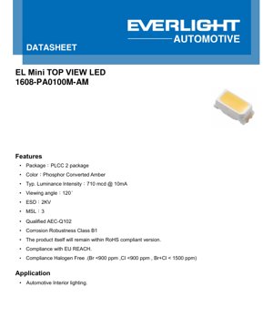
1. Product Overview
This document details the specifications for a compact, high-reliability surface-mount LED designed for demanding applications. The device utilizes a Phosphor Converted (PC) Amber technology within a PLCC-2 (Plastic Leaded Chip Carrier) package, identified by the 1608 footprint (1.6mm x 0.8mm). Its primary design focus is on automotive interior lighting, where consistent performance, color quality, and long-term reliability under varying environmental conditions are paramount. The product is qualified to the AEC-Q102 standard for discrete optoelectronic devices in automotive applications, ensuring it meets stringent quality and reliability requirements for use in vehicles.
2. In-Depth Technical Parameter Analysis
2.1 Photometric and Color Characteristics
The LED's core performance is defined by its photometric output. Under standard test conditions (Forward Current, IF = 10mA, solder pad temperature = 25°C), the typical luminous intensity is 710 millicandelas (mcd). The minimum and maximum values are specified as 610 mcd and 970 mcd, respectively, with a measurement tolerance of ±8%. The dominant color is defined by its Chromaticity Coordinates on the CIE 1931 diagram, with typical values of x=0.56 and y=0.42, representing a specific shade of amber. The tolerance for these coordinates is ±0.005, ensuring tight color consistency between units. The device offers a wide viewing angle of 120 degrees (typical, with a tolerance of ±5°), providing broad, even illumination suitable for panel lighting and indicators.
2.2 Electrical and Thermal Parameters
The electrical characteristics define the operating window. The typical forward voltage (VF) is 2.85V at 10mA, with a range from 2.5V (min) to 3.5V (max). The absolute maximum continuous forward current is 20mA, with a surge current capability of 50mA for pulses ≤10μs. The device is not designed for reverse bias operation. Thermal management is critical for LED longevity. The thermal resistance from the semiconductor junction to the solder point is specified using two methods: 160 K/W (real, based on optical measurement) and 140 K/W (electrical, based on VF measurement). The maximum permissible junction temperature (TJ) is 125°C, with an operating ambient temperature range of -40°C to +110°C.
2.3 Absolute Maximum Ratings and Reliability
Operating beyond these limits may cause permanent damage. Key ratings include a power dissipation (Pd) of 70mW, the aforementioned forward current and temperature limits, and an ESD sensitivity rating of 2kV (Human Body Model). The device is rated for reflow soldering at a peak temperature of 260°C for 30 seconds. It complies with RoHS, EU REACH, and is halogen-free (Br <900ppm, Cl <900ppm, Br+Cl <1500ppm). It also meets Corrosion Robustness Class B1 and has a Moisture Sensitivity Level (MSL) of 3.
3. Binning System Explanation
To manage production variations and allow for precise selection, the LEDs are sorted into bins for key parameters.
3.1 Luminous Intensity Binning
Luminous intensity is grouped into bins labeled from Q to B, with each group containing sub-bins X, Y, Z. For this specific part number (1608-PA0100M-AM), the typical output of 710 mcd falls within the VZ bin, which covers the range from 970 mcd (min) to 1120 mcd (max). The datasheet highlights that the "possible output bins" for this product are centered around this VZ range, as indicated in the table.
3.2 Color Binning
The Phosphor Converted Amber color is binned according to specific regions on the CIE chromaticity chart. The datasheet provides the coordinate boundaries for three primary bins: 8285, 8588, and 8891. Each bin is defined by a set of three or four coordinate points that form a polygon on the x,y chart. The typical color coordinates (x=0.56, y=0.42) for this LED fall within the 8588 bin, which is bounded by the points (0.5448, 0.4544), (0.5633, 0.4361), (0.5250, 0.4450), and (0.5080, 0.4620). The tolerance for color coordinates within a bin is ±0.005.
3.3 Forward Voltage Binning
Forward voltage is binned in 0.25V steps, with bin codes ranging from 1012 (1.00V - 1.25V) up to 6770 (6.75V - 7.00V). The typical VF of 2.85V for this LED would place it in the 2730 bin (2.75V - 3.00V). This binning allows designers to select LEDs with closely matched voltage drops for current-sharing in multi-LED arrays.
4. Performance Curve Analysis
4.1 Spectral Distribution and Radiation Pattern
The relative spectral distribution graph shows a broad emission peak characteristic of phosphor-converted LEDs. The amber light is generated by a blue-emitting chip exciting a phosphor layer, which down-converts part of the blue light to longer wavelengths (yellow/red), resulting in the final amber color. The typical radiation pattern diagram is Lambertian-like, confirming the 120° viewing angle where intensity falls to half of its peak value at ±60° off-axis.
4.2 Forward Current vs. Forward Voltage (I-V Curve)
The I-V curve is non-linear, as expected for a diode. The graph shows the relationship between forward current (IF) and forward voltage (VF). This curve is essential for designing the current-limiting circuitry. The voltage increases with current, starting around 2.4V at very low currents and reaching approximately 3.2V at the maximum rated 20mA.
4.3 Relative Luminous Intensity vs. Forward Current
This graph demonstrates the light output's dependence on drive current. The relative luminous intensity increases super-linearly with current up to a point. This relationship is crucial for dimming and brightness control design, showing that output does not scale linearly with current, especially at lower currents.
4.4 Temperature Dependency Characteristics
Several graphs illustrate the impact of temperature on performance. The Relative Luminous Intensity vs. Junction Temperature graph shows that light output decreases as junction temperature rises. At 110°C, the output is roughly 60-70% of its value at 25°C. The Relative Forward Voltage vs. Junction Temperature graph shows VF decreases linearly with increasing temperature (approximately -2mV/°C), which can be used for junction temperature estimation. The Chromaticity Shift vs. Junction Temperature graph indicates minor but measurable movement in color coordinates (Δx, Δy) with temperature, which is important for color-critical applications.
4.5 Forward Current Derating and Pulse Handling
The Forward Current Derating Curve is vital for reliability. It shows the maximum allowable continuous forward current as a function of the solder pad temperature. As pad temperature increases, the maximum safe current decreases linearly. At the maximum operating pad temperature of 110°C, the maximum current is 20mA. The graph also specifies not to use currents below 2mA. The Permissible Pulse Handling Capability chart defines the peak current allowed for short pulses at various duty cycles (D). For very short pulses (e.g., 0.1ms) at low duty cycles (e.g., 0.5%), currents significantly higher than the DC maximum (up to ~55mA) can be tolerated.
5. Mechanical, Assembly, and Packaging Information
5.1 Mechanical Dimensions and Polarity
The LED uses a standard PLCC-2 surface-mount package with a 1608 footprint. The mechanical drawing (implied in the contents) would specify the exact length, width, height, lead dimensions, and tolerances. The package includes a molded lens. Polarity is indicated by a cathode mark, typically a notch, green dot, or other marking on the package body, which must be aligned with the corresponding marking on the PCB silkscreen or footprint.
5.2 Recommended Soldering Pad Layout and Reflow Profile
A recommended land pattern (solder pad design) is provided to ensure proper soldering, mechanical stability, and thermal performance. This pattern typically includes pads for the two electrical contacts and may include thermal relief connections. The Reflow Soldering Profile specifies the time-temperature requirements for soldering. The key parameter is a peak temperature of 260°C for 30 seconds maximum. The profile will also include preheat, soak, and cooling ramp rates to prevent thermal shock and ensure reliable solder joints.
5.3 Packaging and Handling Precautions
Packaging information details the tape and reel specifications used for automated assembly, including reel dimensions, pocket spacing, and orientation. Due to its MSL 3 rating, the device must be baked if the moisture barrier bag is opened and the components are exposed to ambient conditions for longer than the specified floor life (typically 168 hours) before reflow soldering. General precautions include avoiding mechanical stress on the lens, using proper ESD handling procedures, and following the recommended soldering profile to prevent damage.
6. Application Guidelines and Design Considerations
6.1 Primary Application: Automotive Interior Lighting
The stated application is automotive interior lighting. This encompasses a wide range of uses such as dashboard backlighting, switch illumination, ambient lighting, footwell lights, and console indicators. The AEC-Q102 qualification, wide temperature range (-40°C to +110°C), and corrosion resistance make it suitable for the harsh environment inside a vehicle.
6.2 Circuit Design Considerations
Current Drive: LEDs are current-driven devices. A constant current source or a current-limiting resistor in series with a voltage source is mandatory. The design must ensure the forward current does not exceed the absolute maximum rating, considering the derating curve at elevated temperatures.
Thermal Management: The thermal resistance from junction to solder point is significant (140-160 K/W). To maintain a low junction temperature and ensure long life and stable color, the PCB must act as an effective heat sink. This involves using adequate copper area under and around the LED pad, thermal vias to inner layers, and possibly connecting to a metal core or chassis.
ESD Protection: With an ESD rating of 2kV HBM, basic ESD precautions during handling and assembly are sufficient. For applications in environments with higher ESD risk, additional protection circuitry on the PCB may be considered.
Dimming: For brightness control, Pulse Width Modulation (PWM) is preferred over analog current dimming. PWM maintains a constant current during the "on" pulse, preserving the LED's chromaticity, whereas analog dimming (reducing current) can cause a noticeable color shift, as shown in the Chromaticity Shift vs. Forward Current graph.
7. Technical Comparison and Differentiation
Compared to a standard amber LED chip without phosphor conversion, this PC Amber LED typically offers a broader spectrum and potentially higher color rendering in the amber region, which may be desirable for certain interior lighting aesthetics. The PLCC-2 package provides a more robust and easier-to-handle SMT solution compared to chip-scale packages (CSP), with better light extraction due to the molded lens. The AEC-Q102 qualification and specified sulfur test criteria (mentioned in the contents) are key differentiators for automotive use versus commercial-grade LEDs, addressing long-term reliability under thermal cycling, humidity, and chemical exposure found in vehicles.
8. Frequently Asked Questions (Based on Technical Parameters)
Q: What is the typical drive current for this LED?
A: The standard test condition and typical performance data are given at IF = 10mA. It can be operated anywhere between the minimum (2mA) and maximum (20mA) ratings, with output and efficiency varying accordingly.
Q: How do I control the brightness?
A: Brightness is primarily controlled by the forward current. For smooth dimming over a wide range without color shift, Pulse Width Modulation (PWM) is recommended. Refer to the Relative Luminous Intensity vs. Forward Current graph for the relationship.
Q: Why is the luminous intensity given as a range (bin)?
A: Due to inherent variations in semiconductor and phosphor manufacturing, LEDs are sorted (binned) after production. Specifying a bin (e.g., VZ) guarantees the luminous intensity will fall within a known, tight range, allowing for consistent system design.
Q: Can I use this LED outdoors?
A: While it has a wide temperature range, its primary qualification and application focus is automotive interior lighting. For exterior use, additional considerations like UV resistance of the lens, waterproofing, and potentially higher temperature extremes would need evaluation.
Q: What is the purpose of the "Forward Current Derating Curve"?
A: This curve is critical for reliability. It defines the maximum safe continuous current the LED can handle at a given operating temperature (solder pad temperature). Exceeding this curve increases the junction temperature beyond its maximum rating (125°C), drastically reducing lifespan and potentially causing immediate failure.
9. Design and Usage Case Example
Scenario: Designing an automotive dashboard backlight for a warning indicator.
Step 1 - Electrical Design: The system voltage is 12V (automotive battery). To achieve the desired brightness, a drive current of 10mA is selected. Using the typical VF of 2.85V, a series current-limiting resistor is calculated: R = (Vsupply - VF) / IF = (12V - 2.85V) / 0.01A = 915 Ohms. A standard 910 Ohm resistor is chosen. The resistor power rating is P = I2R = (0.01)2 * 910 = 0.091W, so a 1/8W or 1/10W resistor is sufficient.
Step 2 - Thermal Design: The maximum ambient temperature near the dashboard PCB is estimated at 85°C. Using the derating curve, the maximum allowable current at a pad temperature of 85°C is approximately 22mA. Since the operating current (10mA) is well below this, thermal design is adequate. However, a small copper pour connected to the LED's thermal pad is still added to the PCB layout to help dissipate heat.
Step 3 - Layout: The recommended solder pad footprint is used. The PCB silkscreen clearly marks the cathode side of the footprint to match the notch on the LED package. ESD-sensitive assembly procedures are followed.
10. Technology Principle Introduction
This LED is based on Phosphor Conversion (PC) technology. The core of the device is a semiconductor chip, typically made of Indium Gallium Nitride (InGaN), which emits light in the blue spectrum when electrical current passes through it. This blue light is not the final output. Instead, it is directed onto a layer of phosphor material deposited inside the package. Phosphors are inorganic compounds that exhibit photoluminescence. When the high-energy blue photons strike the phosphor, they are absorbed, exciting the phosphor's electrons. As these electrons return to their ground state, they emit lower-energy photons, primarily in the yellow and red regions of the spectrum. The combination of the unconverted blue light from the chip and the converted yellow/red light from the phosphor mixes to produce the perceived amber color. This method allows for the creation of specific color points (like the defined amber bins) that are difficult or inefficient to achieve with direct semiconductor emission alone.
11. Industry Trends and Developments
The market for automotive interior lighting LEDs is driven by several key trends. There is a continuous push for higher efficiency (lumens per watt) to reduce power consumption and thermal load, especially as vehicles incorporate more electronic features. Miniaturization remains important, with packages like 1608 (and smaller) enabling sleeker, more integrated designs. Enhanced color quality and consistency are critical for premium interior aesthetics, leading to tighter color binning and improved phosphor technology for stability over temperature and lifetime. Increased functionality is emerging, such as integrating multiple color LEDs (e.g., RGB) into a single package for dynamic ambient lighting systems. Furthermore, reliability standards like AEC-Q102 are becoming the baseline expectation, with future developments likely focusing on even more rigorous testing for longer lifetimes and harsher environmental conditions, including resistance to new types of contaminants found in modern vehicle interiors.
LED Specification Terminology
Complete explanation of LED technical terms
Photoelectric Performance
| Term | Unit/Representation | Simple Explanation | Why Important |
|---|---|---|---|
| Luminous Efficacy | lm/W (lumens per watt) | Light output per watt of electricity, higher means more energy efficient. | Directly determines energy efficiency grade and electricity cost. |
| Luminous Flux | lm (lumens) | Total light emitted by source, commonly called "brightness". | Determines if the light is bright enough. |
| Viewing Angle | ° (degrees), e.g., 120° | Angle where light intensity drops to half, determines beam width. | Affects illumination range and uniformity. |
| CCT (Color Temperature) | K (Kelvin), e.g., 2700K/6500K | Warmth/coolness of light, lower values yellowish/warm, higher whitish/cool. | Determines lighting atmosphere and suitable scenarios. |
| CRI / Ra | Unitless, 0–100 | Ability to render object colors accurately, Ra≥80 is good. | Affects color authenticity, used in high-demand places like malls, museums. |
| SDCM | MacAdam ellipse steps, e.g., "5-step" | Color consistency metric, smaller steps mean more consistent color. | Ensures uniform color across same batch of LEDs. |
| Dominant Wavelength | nm (nanometers), e.g., 620nm (red) | Wavelength corresponding to color of colored LEDs. | Determines hue of red, yellow, green monochrome LEDs. |
| Spectral Distribution | Wavelength vs intensity curve | Shows intensity distribution across wavelengths. | Affects color rendering and quality. |
Electrical Parameters
| Term | Symbol | Simple Explanation | Design Considerations |
|---|---|---|---|
| Forward Voltage | Vf | Minimum voltage to turn on LED, like "starting threshold". | Driver voltage must be ≥Vf, voltages add up for series LEDs. |
| Forward Current | If | Current value for normal LED operation. | Usually constant current drive, current determines brightness & lifespan. |
| Max Pulse Current | Ifp | Peak current tolerable for short periods, used for dimming or flashing. | Pulse width & duty cycle must be strictly controlled to avoid damage. |
| Reverse Voltage | Vr | Max reverse voltage LED can withstand, beyond may cause breakdown. | Circuit must prevent reverse connection or voltage spikes. |
| Thermal Resistance | Rth (°C/W) | Resistance to heat transfer from chip to solder, lower is better. | High thermal resistance requires stronger heat dissipation. |
| ESD Immunity | V (HBM), e.g., 1000V | Ability to withstand electrostatic discharge, higher means less vulnerable. | Anti-static measures needed in production, especially for sensitive LEDs. |
Thermal Management & Reliability
| Term | Key Metric | Simple Explanation | Impact |
|---|---|---|---|
| Junction Temperature | Tj (°C) | Actual operating temperature inside LED chip. | Every 10°C reduction may double lifespan; too high causes light decay, color shift. |
| Lumen Depreciation | L70 / L80 (hours) | Time for brightness to drop to 70% or 80% of initial. | Directly defines LED "service life". |
| Lumen Maintenance | % (e.g., 70%) | Percentage of brightness retained after time. | Indicates brightness retention over long-term use. |
| Color Shift | Δu′v′ or MacAdam ellipse | Degree of color change during use. | Affects color consistency in lighting scenes. |
| Thermal Aging | Material degradation | Deterioration due to long-term high temperature. | May cause brightness drop, color change, or open-circuit failure. |
Packaging & Materials
| Term | Common Types | Simple Explanation | Features & Applications |
|---|---|---|---|
| Package Type | EMC, PPA, Ceramic | Housing material protecting chip, providing optical/thermal interface. | EMC: good heat resistance, low cost; Ceramic: better heat dissipation, longer life. |
| Chip Structure | Front, Flip Chip | Chip electrode arrangement. | Flip chip: better heat dissipation, higher efficacy, for high-power. |
| Phosphor Coating | YAG, Silicate, Nitride | Covers blue chip, converts some to yellow/red, mixes to white. | Different phosphors affect efficacy, CCT, and CRI. |
| Lens/Optics | Flat, Microlens, TIR | Optical structure on surface controlling light distribution. | Determines viewing angle and light distribution curve. |
Quality Control & Binning
| Term | Binning Content | Simple Explanation | Purpose |
|---|---|---|---|
| Luminous Flux Bin | Code e.g., 2G, 2H | Grouped by brightness, each group has min/max lumen values. | Ensures uniform brightness in same batch. |
| Voltage Bin | Code e.g., 6W, 6X | Grouped by forward voltage range. | Facilitates driver matching, improves system efficiency. |
| Color Bin | 5-step MacAdam ellipse | Grouped by color coordinates, ensuring tight range. | Guarantees color consistency, avoids uneven color within fixture. |
| CCT Bin | 2700K, 3000K etc. | Grouped by CCT, each has corresponding coordinate range. | Meets different scene CCT requirements. |
Testing & Certification
| Term | Standard/Test | Simple Explanation | Significance |
|---|---|---|---|
| LM-80 | Lumen maintenance test | Long-term lighting at constant temperature, recording brightness decay. | Used to estimate LED life (with TM-21). |
| TM-21 | Life estimation standard | Estimates life under actual conditions based on LM-80 data. | Provides scientific life prediction. |
| IESNA | Illuminating Engineering Society | Covers optical, electrical, thermal test methods. | Industry-recognized test basis. |
| RoHS / REACH | Environmental certification | Ensures no harmful substances (lead, mercury). | Market access requirement internationally. |
| ENERGY STAR / DLC | Energy efficiency certification | Energy efficiency and performance certification for lighting. | Used in government procurement, subsidy programs, enhances competitiveness. |