Table of Contents
- 1. Product Overview
- 1.1 Core Advantages
- 1.2 Target Market and Applications
- 2. In-Depth Technical Parameter Analysis
- 2.1 Photometric and Electrical Characteristics
- 2.2 Absolute Maximum Ratings
- 2.3 Thermal Characteristics
- 3. Binning System Explanation
- 3.1 Luminous Intensity Binning
- 3.2 Chromaticity Coordinate Binning
- 4. Performance Curve Analysis
- 4.1 IV Curve and Relative Luminous Intensity
- 4.2 Temperature Dependence
- 4.3 Spectral Distribution and Pulse Handling
- 5. Mechanical and Package Information
- 5.1 Mechanical Dimensions
- 5.2 Recommended Soldering Pad Layout and Polarity
- 6. Soldering and Assembly Guidelines
- 6.1 Reflow Soldering Profile
- 6.2 Precautions for Use and Storage
- 7. Packaging and Ordering Information
- 7.1 Packaging Specifications
- 7.2 Part Number and Ordering Code
- 8. Application Design Recommendations
- 8.1 Typical Application Circuits
- 8.2 Thermal Management Considerations
- 8.3 Optical Design Considerations
- 9. Technical Comparison and Differentiation
- 10. Frequently Asked Questions (FAQ)
- 10.1 What is the recommended drive current?
- 10.2 How do I interpret the luminous intensity bin code?
- 10.3 Can this LED be used for PWM dimming?
- 11. Practical Design Case Study
- 12. Operating Principle
- 13. Technology Trends
- LED Specification Terminology
- Photoelectric Performance
- Electrical Parameters
- Thermal Management & Reliability
- Packaging & Materials
- Quality Control & Binning
- Testing & Certification
1. Product Overview
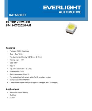
This document details the specifications for a high-performance, surface-mount LED in a PLCC-2 package. The device emits a cool white light and is engineered for reliability and performance in demanding environments. Its primary design focus is automotive interior applications, where consistent light output, wide viewing angles, and robust construction are paramount. The LED meets stringent automotive qualification standards, ensuring long-term performance under variable thermal and electrical conditions.
1.1 Core Advantages
The LED offers several key advantages for design engineers. The typical luminous intensity of 2240 millicandelas (mcd) at a standard 20mA drive current provides bright illumination. A wide 120-degree viewing angle ensures uniform light distribution, which is critical for panel and switch backlighting. The device is qualified to the AEC-Q102 standard, confirming its suitability for automotive use. Furthermore, it complies with major environmental regulations including RoHS, REACH, and Halogen-Free requirements, supporting global manufacturing and sustainability goals. It also features sulfur robustness (Class B1), enhancing its longevity in environments with atmospheric contaminants.
1.2 Target Market and Applications
The primary target market is the automotive electronics sector. Specific applications include interior ambient lighting, backlighting for instrument clusters, and illumination for various switches and control panels. The combination of optical performance, reliability, and compliance makes it an ideal choice for these applications.
2. In-Depth Technical Parameter Analysis
A thorough understanding of the electrical, optical, and thermal parameters is essential for proper circuit design and thermal management.
2.1 Photometric and Electrical Characteristics
The key operating point is defined at a forward current (IF) of 20mA. At this current, the typical luminous intensity (IV) is 2240 mcd, with a minimum of 1400 mcd and a maximum of 3550 mcd, indicating the production spread. The forward voltage (VF) typically measures 3.1V, ranging from 2.5V to 3.75V. The dominant wavelength is characterized by CIE 1931 chromaticity coordinates, with a typical value of (0.3, 0.3). The viewing angle, where luminous intensity drops to half of its peak value, is 120 degrees with a tolerance of ±5°.
2.2 Absolute Maximum Ratings
These ratings define the stress limits beyond which permanent damage may occur. The maximum continuous forward current is 80 mA. The device can withstand a surge current of 250 mA for very short pulses (t ≤ 10 μs, duty cycle D=0.005). The maximum power dissipation is 300 mW. The junction temperature must not exceed 125°C, with an operating temperature range of -40°C to +110°C. The Electrostatic Discharge (ESD) sensitivity, tested per the Human Body Model (HBM), is rated at 8 kV. The maximum soldering temperature during reflow is 260°C for 30 seconds.
2.3 Thermal Characteristics
Thermal management is crucial for LED longevity and light output stability. The datasheet specifies two thermal resistance values: the real thermal resistance from junction to solder point (Rth JS real) is a maximum of 130 K/W, while the electrical method-derived value (Rth JS el) is a maximum of 100 K/W. Designers should use the real value for accurate thermal modeling. The forward current derating curve shows that the maximum allowable continuous current decreases as the solder pad temperature increases, dropping to 31 mA at 110°C.
3. Binning System Explanation
To manage production variations, LEDs are sorted into bins based on key parameters.
3.1 Luminous Intensity Binning
The luminous intensity is binned using an alphanumeric code system (e.g., L1, M2, BA, CB). The bins cover a wide range from a minimum of 11.2 mcd (L1) to over 22,400 mcd (GA). The typical part (2240 mcd) falls into the \"BA\" bin, which spans from 1800 mcd to 2240 mcd. The highlighted bins in the datasheet table indicate the possible output range for this specific product.
3.2 Chromaticity Coordinate Binning
The cool white color is defined within specific regions on the CIE 1931 chromaticity diagram. The datasheet provides a graphical bin structure and lists specific bin codes (e.g., FK0, GK0, HK0, NK0, PK0, FL0) with their corresponding coordinate boundaries. This ensures color consistency within a defined tolerance for applications requiring uniform appearance.
4. Performance Curve Analysis
Graphical data provides insight into the LED's behavior under different operating conditions.
4.1 IV Curve and Relative Luminous Intensity
The Forward Current vs. Forward Voltage graph shows the exponential relationship typical of diodes. The Relative Luminous Intensity vs. Forward Current curve is sub-linear; intensity increases with current but not proportionally, and efficiency may drop at higher currents due to increased heat.
4.2 Temperature Dependence
The Relative Forward Voltage vs. Junction Temperature graph has a negative slope, meaning VF decreases as temperature rises, which is characteristic of the semiconductor bandgap. The Relative Luminous Intensity vs. Junction Temperature graph shows intensity decreasing as temperature increases, a phenomenon known as thermal droop. The Chromaticity Coordinates Shift vs. Junction Temperature graph indicates how the white point may change slightly with temperature, which is important for color-critical applications.
4.3 Spectral Distribution and Pulse Handling
The Relative Spectral Distribution graph depicts the emission spectrum of the cool white phosphor-converted LED, showing a blue pump peak and a broad yellow phosphor emission. The Permissible Pulse Handling Capability chart defines the maximum allowable non-continuous pulse current for various duty cycles and pulse widths, useful for multiplexing or PWM dimming applications.
5. Mechanical and Package Information
5.1 Mechanical Dimensions
The LED uses a standard PLCC-2 (Plastic Leaded Chip Carrier) surface-mount package. The dimensional drawing provides critical measurements including overall length, width, height, lead spacing, and pad sizes. Adherence to these dimensions is necessary for PCB footprint design and automated assembly.
5.2 Recommended Soldering Pad Layout and Polarity
A recommended land pattern (solder pad design) is provided to ensure reliable solder joints and proper alignment during reflow. The polarity is indicated by the package morphology; typically, one lead or a notch/cutout on the package body denotes the cathode. Correct orientation is essential for circuit operation.
6. Soldering and Assembly Guidelines
6.1 Reflow Soldering Profile
A detailed reflow soldering temperature profile is specified. The peak temperature must not exceed 260°C, and the time above 240°C (or similar liquidus temperature) should be limited to the recommended duration (e.g., 30 seconds) to prevent thermal damage to the plastic package and the internal die and wire bonds.
6.2 Precautions for Use and Storage
General handling precautions include avoiding mechanical stress on the lens, protecting from electrostatic discharge (ESD) using appropriate grounding, and storing in a dry, controlled environment. The device is not designed for reverse bias operation. The storage temperature range matches the operating range (-40°C to +110°C).
7. Packaging and Ordering Information
7.1 Packaging Specifications
The LEDs are supplied in industry-standard tape and reel packaging suitable for automated pick-and-place machines. The packaging information details the reel dimensions, tape width, pocket spacing, and orientation of components within the tape.
7.2 Part Number and Ordering Code
The base part number is 67-11-C70202H-AM. The ordering information may include options for specifying different bins for luminous intensity or chromaticity coordinates, allowing designers to select the precise performance grade required for their application.
8. Application Design Recommendations
8.1 Typical Application Circuits
For constant light output, drive the LED with a constant current source, not a constant voltage. A simple series resistor can be used with a stable voltage supply, but its value must be calculated based on the supply voltage, the LED's forward voltage (using max VF for worst-case current calculation), and the desired current (e.g., 20mA). For automotive applications, consider transient voltage suppression and reverse polarity protection on the input.
8.2 Thermal Management Considerations
To maintain performance and lifetime, manage the heat at the solder pad. Use the thermal resistance value (Rth JS real = 130 K/W max) to calculate the junction temperature rise: ΔTJ = PD * Rth JS, where PD = VF * IF. Ensure the calculated TJ remains below 125°C. Adequate copper pour on the PCB under and around the LED pads acts as a heat sink.
8.3 Optical Design Considerations
The 120° viewing angle is a full width at half maximum (FWHM) value. For applications requiring a narrower beam, secondary optics (lenses) may be needed. The typical CIE coordinates (0.3, 0.3) correspond to a cool white point. If multiple LEDs are used in an array, select parts from the same or adjacent chromaticity bins to avoid visible color mismatch.
9. Technical Comparison and Differentiation
Compared to generic non-automotive PLCC-2 LEDs, this device's key differentiators are its AEC-Q102 qualification, sulfur robustness, and guaranteed performance over the extended automotive temperature range (-40°C to +110°C). The typical luminous intensity of 2240mcd is competitive for its package size and drive current. The comprehensive binning structure allows for tighter system-level performance control.
10. Frequently Asked Questions (FAQ)
10.1 What is the recommended drive current?
The standard test and typical operating condition is 20mA. The maximum continuous current is 80mA, but operating above 20mA will increase junction temperature and may reduce luminous efficacy and long-term reliability. Always refer to the derating curve when operating at elevated ambient temperatures.
10.2 How do I interpret the luminous intensity bin code?
The bin code (e.g., BA) defines a minimum and maximum luminous intensity range. When ordering, you can specify a bin code to ensure you receive LEDs with intensity within that specific range, which is crucial for achieving uniform brightness in a multi-LED design.
10.3 Can this LED be used for PWM dimming?
Yes, the LED can be dimmed using Pulse Width Modulation (PWM). The Permissible Pulse Handling Capability chart should be consulted to ensure the peak current and duty cycle of the PWM signal do not exceed the specified limits. PWM frequency should be high enough to avoid visible flicker (typically >200Hz).
11. Practical Design Case Study
Consider designing backlighting for an automotive climate control panel using 10 of these LEDs. The design goal is uniform brightness at an ambient temperature of up to 85°C. Step 1: Select LEDs from the same luminous intensity bin (e.g., BA) and chromaticity bin to ensure consistency. Step 2: Design a constant-current driver circuit providing 20mA per LED. Step 3: Perform thermal analysis: At 20mA and typical VF of 3.1V, power per LED is 62mW. With Rth JS real of 130 K/W, the temperature rise from solder pad to junction is ~8°C. If the PCB design maintains the solder pad at 90°C (5°C above max ambient), the junction temperature would be ~98°C, which is within the 125°C limit. Step 4: Layout the PCB with sufficient copper for heat spreading and follow the recommended pad layout for reliable soldering.
12. Operating Principle
This is a phosphor-converted white LED. The core semiconductor chip emits blue light when forward biased (electroluminescence). This blue light excites a yellow (or yellow and red) phosphor coating on or near the chip. The combination of the remaining blue light and the broad-spectrum yellow light from the phosphor mixes to produce the perception of white light. The specific ratio of blue to phosphor-converted light determines the correlated color temperature (CCT), resulting in the \"cool white\" appearance in this case.
13. Technology Trends
The general trend in automotive LED lighting is towards higher efficacy (more lumens per watt), improved color rendering index (CRI) for better visual appeal, and higher reliability at elevated junction temperatures. Integration of driver electronics and multiple LED chips within a single package is also common for advanced lighting modules. Furthermore, there is a focus on developing LEDs with even greater resistance to harsh environmental factors like sulfur, moisture, and thermal cycling to meet the evolving demands of next-generation vehicles.
LED Specification Terminology
Complete explanation of LED technical terms
Photoelectric Performance
| Term | Unit/Representation | Simple Explanation | Why Important |
|---|---|---|---|
| Luminous Efficacy | lm/W (lumens per watt) | Light output per watt of electricity, higher means more energy efficient. | Directly determines energy efficiency grade and electricity cost. |
| Luminous Flux | lm (lumens) | Total light emitted by source, commonly called "brightness". | Determines if the light is bright enough. |
| Viewing Angle | ° (degrees), e.g., 120° | Angle where light intensity drops to half, determines beam width. | Affects illumination range and uniformity. |
| CCT (Color Temperature) | K (Kelvin), e.g., 2700K/6500K | Warmth/coolness of light, lower values yellowish/warm, higher whitish/cool. | Determines lighting atmosphere and suitable scenarios. |
| CRI / Ra | Unitless, 0–100 | Ability to render object colors accurately, Ra≥80 is good. | Affects color authenticity, used in high-demand places like malls, museums. |
| SDCM | MacAdam ellipse steps, e.g., "5-step" | Color consistency metric, smaller steps mean more consistent color. | Ensures uniform color across same batch of LEDs. |
| Dominant Wavelength | nm (nanometers), e.g., 620nm (red) | Wavelength corresponding to color of colored LEDs. | Determines hue of red, yellow, green monochrome LEDs. |
| Spectral Distribution | Wavelength vs intensity curve | Shows intensity distribution across wavelengths. | Affects color rendering and quality. |
Electrical Parameters
| Term | Symbol | Simple Explanation | Design Considerations |
|---|---|---|---|
| Forward Voltage | Vf | Minimum voltage to turn on LED, like "starting threshold". | Driver voltage must be ≥Vf, voltages add up for series LEDs. |
| Forward Current | If | Current value for normal LED operation. | Usually constant current drive, current determines brightness & lifespan. |
| Max Pulse Current | Ifp | Peak current tolerable for short periods, used for dimming or flashing. | Pulse width & duty cycle must be strictly controlled to avoid damage. |
| Reverse Voltage | Vr | Max reverse voltage LED can withstand, beyond may cause breakdown. | Circuit must prevent reverse connection or voltage spikes. |
| Thermal Resistance | Rth (°C/W) | Resistance to heat transfer from chip to solder, lower is better. | High thermal resistance requires stronger heat dissipation. |
| ESD Immunity | V (HBM), e.g., 1000V | Ability to withstand electrostatic discharge, higher means less vulnerable. | Anti-static measures needed in production, especially for sensitive LEDs. |
Thermal Management & Reliability
| Term | Key Metric | Simple Explanation | Impact |
|---|---|---|---|
| Junction Temperature | Tj (°C) | Actual operating temperature inside LED chip. | Every 10°C reduction may double lifespan; too high causes light decay, color shift. |
| Lumen Depreciation | L70 / L80 (hours) | Time for brightness to drop to 70% or 80% of initial. | Directly defines LED "service life". |
| Lumen Maintenance | % (e.g., 70%) | Percentage of brightness retained after time. | Indicates brightness retention over long-term use. |
| Color Shift | Δu′v′ or MacAdam ellipse | Degree of color change during use. | Affects color consistency in lighting scenes. |
| Thermal Aging | Material degradation | Deterioration due to long-term high temperature. | May cause brightness drop, color change, or open-circuit failure. |
Packaging & Materials
| Term | Common Types | Simple Explanation | Features & Applications |
|---|---|---|---|
| Package Type | EMC, PPA, Ceramic | Housing material protecting chip, providing optical/thermal interface. | EMC: good heat resistance, low cost; Ceramic: better heat dissipation, longer life. |
| Chip Structure | Front, Flip Chip | Chip electrode arrangement. | Flip chip: better heat dissipation, higher efficacy, for high-power. |
| Phosphor Coating | YAG, Silicate, Nitride | Covers blue chip, converts some to yellow/red, mixes to white. | Different phosphors affect efficacy, CCT, and CRI. |
| Lens/Optics | Flat, Microlens, TIR | Optical structure on surface controlling light distribution. | Determines viewing angle and light distribution curve. |
Quality Control & Binning
| Term | Binning Content | Simple Explanation | Purpose |
|---|---|---|---|
| Luminous Flux Bin | Code e.g., 2G, 2H | Grouped by brightness, each group has min/max lumen values. | Ensures uniform brightness in same batch. |
| Voltage Bin | Code e.g., 6W, 6X | Grouped by forward voltage range. | Facilitates driver matching, improves system efficiency. |
| Color Bin | 5-step MacAdam ellipse | Grouped by color coordinates, ensuring tight range. | Guarantees color consistency, avoids uneven color within fixture. |
| CCT Bin | 2700K, 3000K etc. | Grouped by CCT, each has corresponding coordinate range. | Meets different scene CCT requirements. |
Testing & Certification
| Term | Standard/Test | Simple Explanation | Significance |
|---|---|---|---|
| LM-80 | Lumen maintenance test | Long-term lighting at constant temperature, recording brightness decay. | Used to estimate LED life (with TM-21). |
| TM-21 | Life estimation standard | Estimates life under actual conditions based on LM-80 data. | Provides scientific life prediction. |
| IESNA | Illuminating Engineering Society | Covers optical, electrical, thermal test methods. | Industry-recognized test basis. |
| RoHS / REACH | Environmental certification | Ensures no harmful substances (lead, mercury). | Market access requirement internationally. |
| ENERGY STAR / DLC | Energy efficiency certification | Energy efficiency and performance certification for lighting. | Used in government procurement, subsidy programs, enhances competitiveness. |