Table of Contents
- 1. Product Overview
- 2. Technical Parameters Deep Dive
- 2.1 Absolute Maximum Ratings
- 2.2 Electro-Optical Characteristics
- 3. Performance Curve Analysis
- 3.1 Thermal and Optical Characteristics
- 3.2 Current vs. Illumination and Temperature
- 3.3 Capacitance and Response Time
- 4. Mechanical and Package Information
- 5. Soldering and Assembly Guidelines
- 6. Packaging and Ordering Information
- 7. Application Suggestions
- 7.1 Typical Application Scenarios
- 7.2 Design Considerations
- 8. Technical Comparison and Differentiation
- 9. Frequently Asked Questions (Based on Technical Parameters)
- 10. Practical Design Case
- 11. Operating Principle Introduction
- 12. Technology Trends
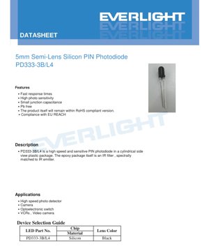
1. Product Overview
The PD333-3B/L4 is a high-speed, high-sensitivity silicon PIN photodiode housed in a cylindrical side-view plastic package. Its defining feature is the integrated epoxy package which also functions as an infrared (IR) filter, making it spectrally matched to common IR emitters. This integration simplifies optical design by reducing the need for external filtering components. The device is designed for applications requiring fast response times and reliable detection of infrared light, particularly in the 940nm wavelength range.
Key advantages include its fast response times, high photosensitivity, and small junction capacitance, which are critical for signal integrity in high-speed applications. The component is compliant with RoHS and EU REACH regulations, and is manufactured using lead-free processes, aligning with modern environmental and safety standards for electronic components.
2. Technical Parameters Deep Dive
2.1 Absolute Maximum Ratings
The device is rated for operation within specific environmental and electrical limits to ensure reliability and prevent damage. The maximum reverse voltage (VR) is 32V. The power dissipation (Pd) rating is 150mW. The component can withstand lead soldering temperatures (Tsol) up to 260°C for a duration not exceeding 5 seconds, which is compatible with standard reflow soldering processes. The operating temperature range (Topr) is from -40°C to +85°C, and the storage temperature range (Tstg) is from -40°C to +100°C, indicating robust performance across a wide range of conditions.
2.2 Electro-Optical Characteristics
The photodiode's performance is characterized under standard conditions (Ta=25°C). Its spectral bandwidth (λ0.5) ranges from 840nm to 1100nm, with peak sensitivity (λp) at 940nm. This makes it ideal for use with 940nm IR LEDs. Key electrical parameters include an open-circuit voltage (VOC) of 0.42V typical when illuminated with 5mW/cm² at 940nm, and a short-circuit current (ISC) of 10µA typical under 1mW/cm² illumination at 940nm.
The reverse light current (IL), which is the photocurrent generated under reverse bias, is 12µA typical (VR=5V, Ee=1mW/cm², λp=940nm). The dark current (Id), a critical parameter for low-light sensitivity, is specified at a maximum of 10nA (VR=10V). The reverse breakdown voltage (BVR) has a minimum of 32V and a typical value of 170V. The total terminal capacitance (Ct) is 5pF typical at VR=5V and 1MHz, a low value contributing to the device's high-speed capability.
3. Performance Curve Analysis
The datasheet provides several characteristic curves that illustrate device behavior under varying conditions. These graphs are essential for design engineers to predict performance in real-world applications beyond the standard test conditions.
3.1 Thermal and Optical Characteristics
Figure 1 shows the relationship between allowable power dissipation and ambient temperature. As temperature increases, the maximum permissible power dissipation decreases linearly, a standard derating characteristic for semiconductor devices. Figure 2 depicts the spectral sensitivity curve, confirming the peak response at 940nm and the defined cutoff points at 840nm and 1100nm where sensitivity drops to half its peak value.
3.2 Current vs. Illumination and Temperature
Figure 3 illustrates how dark current (Id) increases exponentially with rising ambient temperature. This is a fundamental property of semiconductor junctions and is critical for applications operating at elevated temperatures, as increased dark current raises the noise floor. Figure 4 shows the linear relationship between reverse light current (IL) and irradiance (Ee), demonstrating the photodiode's predictable and linear photocurrent generation.
3.3 Capacitance and Response Time
Figure 5 plots terminal capacitance against reverse voltage. Capacitance decreases with increasing reverse bias, a behavior typical of PIN photodiodes. Lower capacitance enables faster response times. Figure 6 shows the relationship between response time and load resistance. The response time increases with higher load resistance due to the RC time constant formed by the junction capacitance and the external load. For high-speed applications, a low-value load resistor (e.g., 50Ω) is typically used, though this trades off signal amplitude for speed.
4. Mechanical and Package Information
The PD333-3B/L4 comes in a cylindrical side-view package. The package body itself is black, which aids in reducing internal reflections and stray light interference. The "semi-lens" design helps to focus incoming light onto the active silicon area, improving effective sensitivity. Detailed package dimensions are provided in the datasheet, with all measurements in millimeters. Critical tolerances for mechanical placement are typically ±0.25mm. The side-view orientation is particularly useful for applications where the light path is parallel to the PCB surface, such as in slot sensors or edge detection systems.
5. Soldering and Assembly Guidelines
The component is suitable for standard PCB assembly processes. The absolute maximum rating for lead soldering temperature is 260°C. It is crucial that the soldering time at this temperature does not exceed 5 seconds to prevent damage to the plastic package or the internal semiconductor die. Standard IR reflow or wave soldering profiles used for lead-free assemblies are generally applicable. Proper handling to avoid contamination of the lens surface is essential for maintaining optical performance. Storage should be within the specified temperature range of -40°C to +100°C in a dry environment.
6. Packaging and Ordering Information
The standard packing specification is 500 pieces per bag, 5 bags per box, and 10 boxes per carton. This bulk packaging is typical for automated assembly lines. The label on the packaging includes critical information for traceability and verification: Customer's Production Number (CPN), Production Number (P/N), Packing Quantity (QTY), quality ranks (CAT), peak wavelength (HUE), a reference code (REF), and the manufacturing Lot Number. The month of production is also indicated. Users should cross-reference the label information with their internal records and the datasheet specifications.
7. Application Suggestions
7.1 Typical Application Scenarios
The PD333-3B/L4 is well-suited for several key applications. As a high-speed photo detector, it can be used in data communication links using infrared light, barcode scanners, or pulse detection systems. Its integration into cameras can be for autofocus assist systems or light metering. In optoelectronic switches, it forms the receiver half of an optical interrupter or reflective sensor, commonly found in printers, encoders, and safety curtains. Its use in VCRs and video cameras historically pertained to tape-end sensors or remote control receivers, though similar principles apply to modern consumer electronics.
7.2 Design Considerations
When designing with this photodiode, several factors must be considered. For biasing, it is typically operated in reverse bias (photoconductive mode) to improve speed and linearity, though photovoltaic mode (zero bias) can be used for low-noise applications. The choice of operational amplifier in the transimpedance amplifier (TIA) circuit is critical; it must have low input bias current and low noise to avoid degrading the signal from the low-dark-current photodiode. The IR-filtering property of the package is beneficial but designers must ensure the source wavelength (e.g., 940nm) aligns with the peak sensitivity. For high-speed operation, careful PCB layout to minimize parasitic capacitance and inductance at the photodiode node is essential.
8. Technical Comparison and Differentiation
Compared to standard photodiodes without an integrated lens or filter, the PD333-3B/L4 offers a more compact and simplified optical solution. The built-in IR filter eliminates the need for a separate filter component, saving space, cost, and assembly complexity. Its side-view package offers a distinct mechanical advantage over top-view packages for specific optical path geometries. The combination of relatively high breakdown voltage (min 32V, typ 170V) and low dark current is a favorable balance for many industrial sensing applications requiring good signal-to-noise ratio and robust operation.
9. Frequently Asked Questions (Based on Technical Parameters)
Q: What is the significance of the peak sensitivity at 940nm?
A: 940nm is a very common wavelength for infrared LEDs because it is invisible to the human eye and has good atmospheric transmission. Matching the photodiode's peak response to the emitter's wavelength maximizes signal strength and system efficiency.
Q: How does the dark current specification affect my design?
A: Dark current is the primary source of noise in a photodiode when no light is present. A low dark current (10nA max for this device) means the sensor can detect very weak light signals without being overwhelmed by its own internal noise, improving sensitivity and dynamic range.
Q: Can I use this for visible light detection?
A> The integrated epoxy package acts as an IR filter, significantly attenuating visible light. Therefore, this specific variant is not suitable for applications requiring sensitivity in the visible spectrum. For visible light detection, a clear or differently filtered package would be required.
Q: What load resistance should I use for optimal speed?
A> Referencing Figure 6, for the fastest response time (in the nanosecond range), a low load resistance (e.g., 50Ω to 100Ω) is necessary. However, this produces a smaller voltage signal. A transimpedance amplifier circuit is often the best solution, providing both high speed and good signal gain.
10. Practical Design Case
Case: Designing an Infrared Proximity Sensor
In a typical proximity sensor, an IR LED pulses light, and the PD333-3B/L4 detects the reflected light from an object. The built-in IR filter is crucial here, as it blocks ambient visible light (e.g., from room lighting) which could saturate the sensor or create false triggers. The fast response time allows for rapid pulsing of the LED, enabling quick detection and potentially allowing for distance measurement via time-of-flight or phase-shift methods in more advanced systems. The side-view package allows both the LED and photodiode to be mounted on the same PCB plane, facing the same direction, which is ideal for reflective sensing. A simple circuit would involve biasing the photodiode with a 5V reverse bias through a large resistor, and using a high-speed comparator or amplifier to detect the current pulse generated when reflected light is present.
11. Operating Principle Introduction
A PIN photodiode is a semiconductor device with a wide, lightly doped intrinsic (I) region sandwiched between a p-type (P) and an n-type (N) region. When reverse-biased, this structure creates a large depletion region. Photons incident on the device with energy greater than the semiconductor's bandgap create electron-hole pairs within this depletion region. The strong electric field present due to the reverse bias swiftly separates these carriers, causing them to drift to the respective contacts, generating a photocurrent that is proportional to the incident light intensity. The wide intrinsic region reduces junction capacitance (enabling high speed) and increases the volume for photon absorption (improving sensitivity), especially for longer wavelengths like infrared where penetration depth is greater.
12. Technology Trends
The trend in photodiode technology continues towards higher integration, lower noise, and greater functionality. This includes the integration of amplification and signal conditioning circuitry on the same chip or in the same package (e.g., photodiode-amplifier combinations). There is also a drive towards devices with even lower dark currents and capacitances for applications in scientific instrumentation, medical imaging, and LiDAR. The use of materials beyond silicon, such as InGaAs, extends sensitivity further into the infrared for telecommunications and gas sensing. Furthermore, packaging innovations aim to provide more precise optical characteristics, such as defined field-of-view (FOV) lenses and even more effective filtering directly in the package, as seen in the PD333-3B/L4.
LED Specification Terminology
Complete explanation of LED technical terms
Photoelectric Performance
| Term | Unit/Representation | Simple Explanation | Why Important |
|---|---|---|---|
| Luminous Efficacy | lm/W (lumens per watt) | Light output per watt of electricity, higher means more energy efficient. | Directly determines energy efficiency grade and electricity cost. |
| Luminous Flux | lm (lumens) | Total light emitted by source, commonly called "brightness". | Determines if the light is bright enough. |
| Viewing Angle | ° (degrees), e.g., 120° | Angle where light intensity drops to half, determines beam width. | Affects illumination range and uniformity. |
| CCT (Color Temperature) | K (Kelvin), e.g., 2700K/6500K | Warmth/coolness of light, lower values yellowish/warm, higher whitish/cool. | Determines lighting atmosphere and suitable scenarios. |
| CRI / Ra | Unitless, 0–100 | Ability to render object colors accurately, Ra≥80 is good. | Affects color authenticity, used in high-demand places like malls, museums. |
| SDCM | MacAdam ellipse steps, e.g., "5-step" | Color consistency metric, smaller steps mean more consistent color. | Ensures uniform color across same batch of LEDs. |
| Dominant Wavelength | nm (nanometers), e.g., 620nm (red) | Wavelength corresponding to color of colored LEDs. | Determines hue of red, yellow, green monochrome LEDs. |
| Spectral Distribution | Wavelength vs intensity curve | Shows intensity distribution across wavelengths. | Affects color rendering and quality. |
Electrical Parameters
| Term | Symbol | Simple Explanation | Design Considerations |
|---|---|---|---|
| Forward Voltage | Vf | Minimum voltage to turn on LED, like "starting threshold". | Driver voltage must be ≥Vf, voltages add up for series LEDs. |
| Forward Current | If | Current value for normal LED operation. | Usually constant current drive, current determines brightness & lifespan. |
| Max Pulse Current | Ifp | Peak current tolerable for short periods, used for dimming or flashing. | Pulse width & duty cycle must be strictly controlled to avoid damage. |
| Reverse Voltage | Vr | Max reverse voltage LED can withstand, beyond may cause breakdown. | Circuit must prevent reverse connection or voltage spikes. |
| Thermal Resistance | Rth (°C/W) | Resistance to heat transfer from chip to solder, lower is better. | High thermal resistance requires stronger heat dissipation. |
| ESD Immunity | V (HBM), e.g., 1000V | Ability to withstand electrostatic discharge, higher means less vulnerable. | Anti-static measures needed in production, especially for sensitive LEDs. |
Thermal Management & Reliability
| Term | Key Metric | Simple Explanation | Impact |
|---|---|---|---|
| Junction Temperature | Tj (°C) | Actual operating temperature inside LED chip. | Every 10°C reduction may double lifespan; too high causes light decay, color shift. |
| Lumen Depreciation | L70 / L80 (hours) | Time for brightness to drop to 70% or 80% of initial. | Directly defines LED "service life". |
| Lumen Maintenance | % (e.g., 70%) | Percentage of brightness retained after time. | Indicates brightness retention over long-term use. |
| Color Shift | Δu′v′ or MacAdam ellipse | Degree of color change during use. | Affects color consistency in lighting scenes. |
| Thermal Aging | Material degradation | Deterioration due to long-term high temperature. | May cause brightness drop, color change, or open-circuit failure. |
Packaging & Materials
| Term | Common Types | Simple Explanation | Features & Applications |
|---|---|---|---|
| Package Type | EMC, PPA, Ceramic | Housing material protecting chip, providing optical/thermal interface. | EMC: good heat resistance, low cost; Ceramic: better heat dissipation, longer life. |
| Chip Structure | Front, Flip Chip | Chip electrode arrangement. | Flip chip: better heat dissipation, higher efficacy, for high-power. |
| Phosphor Coating | YAG, Silicate, Nitride | Covers blue chip, converts some to yellow/red, mixes to white. | Different phosphors affect efficacy, CCT, and CRI. |
| Lens/Optics | Flat, Microlens, TIR | Optical structure on surface controlling light distribution. | Determines viewing angle and light distribution curve. |
Quality Control & Binning
| Term | Binning Content | Simple Explanation | Purpose |
|---|---|---|---|
| Luminous Flux Bin | Code e.g., 2G, 2H | Grouped by brightness, each group has min/max lumen values. | Ensures uniform brightness in same batch. |
| Voltage Bin | Code e.g., 6W, 6X | Grouped by forward voltage range. | Facilitates driver matching, improves system efficiency. |
| Color Bin | 5-step MacAdam ellipse | Grouped by color coordinates, ensuring tight range. | Guarantees color consistency, avoids uneven color within fixture. |
| CCT Bin | 2700K, 3000K etc. | Grouped by CCT, each has corresponding coordinate range. | Meets different scene CCT requirements. |
Testing & Certification
| Term | Standard/Test | Simple Explanation | Significance |
|---|---|---|---|
| LM-80 | Lumen maintenance test | Long-term lighting at constant temperature, recording brightness decay. | Used to estimate LED life (with TM-21). |
| TM-21 | Life estimation standard | Estimates life under actual conditions based on LM-80 data. | Provides scientific life prediction. |
| IESNA | Illuminating Engineering Society | Covers optical, electrical, thermal test methods. | Industry-recognized test basis. |
| RoHS / REACH | Environmental certification | Ensures no harmful substances (lead, mercury). | Market access requirement internationally. |
| ENERGY STAR / DLC | Energy efficiency certification | Energy efficiency and performance certification for lighting. | Used in government procurement, subsidy programs, enhances competitiveness. |