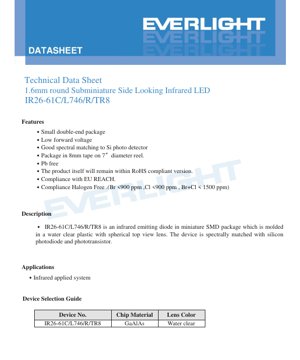
1. Product Overview
The IR26-61C/L746/R/TR8 is a subminiature, side-looking infrared (IR) emitting diode designed for surface-mount applications. This device is housed in a compact, double-ended package molded from water-clear plastic with a spherical lens, optimized for efficient infrared emission. Its spectral output is specifically matched to silicon photodiodes and phototransistors, making it an ideal source for proximity sensing, object detection, and other IR-based systems requiring a reliable and compact emitter.
Key advantages of this component include its very small form factor, low forward voltage operation, and excellent compatibility with standard silicon detectors. The device is supplied on 8mm tape wound onto 7-inch diameter reels, facilitating automated assembly processes. It complies with environmental standards including RoHS, EU REACH, and is halogen-free.
1.1 Device Selection Guide
The device is identified by the part number IR26-61C/L746/R/TR8. It utilizes a GaAlAs (Gallium Aluminum Arsenide) chip material, which is a common semiconductor for producing infrared light. The lens is water-clear, allowing the maximum transmission of the emitted infrared radiation without any filtering or color tinting that could attenuate the signal.
2. Technical Parameter Deep Dive
2.1 Absolute Maximum Ratings
These ratings define the limits beyond which permanent damage to the device may occur. Operation under these conditions is not guaranteed.
- Continuous Forward Current (IF): 65 mA. This is the maximum DC current that can be continuously passed through the LED.
- Reverse Voltage (VR): 5 V. Applying a reverse bias voltage higher than this can break down the LED junction.
- Operating & Storage Temperature (Topr, Tstg): -40°C to +100°C. The device is rated for a wide industrial temperature range.
- Soldering Temperature (Tsol): 260°C for a maximum of 5 seconds. This defines the peak reflow profile tolerance.
- Power Dissipation (Pc): 100 mW at or below 25°C ambient temperature. This limits the total electrical power that can be converted into heat within the package.
2.2 Electro-Optical Characteristics
These parameters are specified at an ambient temperature (Ta) of 25°C and define the typical performance of the device under normal operating conditions.
- Radiant Intensity (IE): The optical power emitted per unit solid angle. Typical values are 8.0 mW/sr at 20mA and can reach 40.0 mW/sr under pulsed operation at 100mA (pulse width ≤100μs, duty cycle ≤1%).
- Peak Wavelength (λp): 940 nm. This is the wavelength at which the LED emits the most optical power, perfectly aligned with the peak sensitivity of many silicon-based detectors.
- Spectral Bandwidth (Δλ): 30 nm (typical). This indicates the range of wavelengths emitted, centered around the peak.
- Forward Voltage (VF): Typically 1.25V with a maximum of 1.50V at 20mA. At 100mA (pulsed), it rises to a typical 1.40V with a maximum of 1.90V. The low VF contributes to higher system efficiency.
- Reverse Current (IR): Maximum 10 μA at a reverse bias of 5V, indicating good junction quality.
- Viewing Angle (2θ1/2): 20 degrees. This is the full angle at which the radiant intensity drops to half of its maximum value (on-axis), defining a relatively narrow, directed beam.
3. Performance Curve Analysis
The datasheet includes several characteristic curves that provide deeper insight into device behavior under varying conditions.
3.1 Forward Current vs. Ambient Temperature
This graph shows the derating of the maximum allowable forward current as the ambient temperature increases. To prevent overheating and ensure reliability, the forward current must be reduced when operating above 25°C. The curve typically shows a linear decrease from the rated 65mA at 25°C down to zero at the maximum junction temperature.
3.2 Spectral Distribution
The spectral output curve illustrates the relative radiant intensity across wavelengths. It confirms the 940nm peak and the approximately 30nm bandwidth, showing a Gaussian-like distribution common for LED sources.
3.3 Radiant Intensity vs. Forward Current
This plot demonstrates the relationship between drive current and optical output. It is generally linear in the lower current range but may show signs of saturation or efficiency droop at very high currents due to thermal and other non-linear effects within the semiconductor.
3.4 Forward Current vs. Forward Voltage
The IV characteristic curve is essential for circuit design. It shows the exponential relationship typical of a diode. The specified VF values at 20mA and 100mA are points on this curve. Designers use this to calculate the necessary current-limiting resistor value for a given supply voltage.
3.5 Relative Radiant Intensity vs. Angular Displacement
This polar plot visually defines the radiation pattern or beam profile of the LED. For this side-looking device with a 20-degree viewing angle, the plot will show a lobe of light emitted perpendicular to the mounting plane, with intensity dropping sharply outside the ±10-degree half-angle.
4. Mechanical and Packaging Information
4.1 Package Dimensions and Polarity
The LED is a 1.6mm round package. Detailed mechanical drawings provide exact dimensions for the body, leads, and lens. The anode and cathode are clearly identified in the diagram. The recommended soldering pad pattern (land pattern) is also provided to ensure proper mechanical and thermal connection during PCB assembly, minimizing stress on the component.
4.2 Carrier Tape and Reel Specifications
The device is packaged for automated placement. The carrier tape dimensions (pocket size, pitch, etc.) and reel specifications (7-inch diameter, 1500 pieces per reel) are detailed to ensure compatibility with standard pick-and-place equipment.
5. Soldering and Assembly Guidelines
5.1 Critical Precautions
- Over-current Protection: An external current-limiting resistor is mandatory. The LED's exponential IV characteristic means a small increase in voltage can cause a large, destructive increase in current.
- Storage: The device is moisture-sensitive (MSL). Unopened bags must be stored at ≤30°C and ≤90% RH and used within one year. After opening, parts must be used within 168 hours (7 days) when stored at ≤30°C/≤70% RH. Exceeding these limits requires baking at 60±5°C for at least 24 hours before use.
5.2 Soldering Conditions
- Reflow Soldering: A Pb-free temperature profile is referenced. Reflow should not be performed more than two times to avoid thermal damage to the plastic package and wire bonds.
- Hand Soldering: If necessary, use a soldering iron tip temperature below 350°C for a maximum of 3 seconds per terminal. Use an iron with a capacity of 25W or less and allow a cooling interval of at least 2 seconds between terminals.
- Repair: Avoid rework after soldering. If unavoidable, a double-head soldering iron must be used to simultaneously heat both terminals, preventing mechanical stress from lifting one pad while the other is still soldered.
6. Packaging and Ordering Information
The final packaging involves sealing the reels in aluminum moisture-proof bags with desiccant. The label on the bag contains critical information for traceability and use: Customer Part Number (CPN), Manufacturer Part Number (P/N), Quantity (QTY), performance ranks (CAT), peak wavelength (HUE), reference codes, lot number (LOT No.), and country of origin.
7. Application Suggestions
7.1 Typical Application Scenarios
This IR LED is designed for infrared applied systems. Its key characteristics make it suitable for:
- Proximity and Presence Sensing: Paired with a phototransistor or photodiode to detect the presence or absence of an object within a short range.
- Object Counting and Edge Detection: In automation equipment to count items on a conveyor or detect edges.
- Optical Switches and Encoders: Where an infrared beam is interrupted by a moving part to generate a digital signal.
- Short-Range Data Transmission: In simple IR communication links (e.g., remote controls, IRDA), though its narrow beam may require careful alignment.
7.2 Design Considerations
- Drive Circuit: Always use a series resistor to set the forward current. Calculate the resistor value as R = (Vcc - Vf) / If, where Vcc is the supply voltage, Vf is the forward voltage from the datasheet (use max value for a safe design), and If is the desired forward current (e.g., 20mA).
- Thermal Management: For continuous operation near the maximum current rating, consider the PCB layout's ability to dissipate heat from the LED's pads.
- Optical Alignment: The 20-degree viewing angle and side-looking orientation require precise mechanical design to ensure the IR beam is directed correctly towards the detector.
- Ambient Light Immunity: For sensing applications, consider using modulated IR signals and synchronous detection in the receiver to reject ambient light noise, especially from sources like sunlight or fluorescent lamps that contain IR components.
8. Technical Comparison and Differentiation
Compared to standard top-emitting IR LEDs, the side-looking package offers a distinct mechanical advantage. It allows the IR beam to be emitted parallel to the PCB surface, which can simplify optical path design in space-constrained applications where the emitter and detector need to be placed on the same plane, facing each other across a gap. Its 1.6mm diameter and low profile make it one of the smaller SMD IR emitters available, suitable for miniaturized devices. The combination of GaAlAs chip technology, 940nm wavelength, and clear lens provides high efficiency and good matching to silicon detectors without the attenuation caused by colored (e.g., blue or black) epoxy lenses sometimes used for visible-light blocking.
9. Frequently Asked Questions (FAQ)
9.1 What is the purpose of the \"water clear\" lens?
The water-clear lens has minimal absorption across the visible and infrared spectrum. For an IR LED, this maximizes the transmission of the 940nm infrared light out of the package. It does not filter visible light, but since the chip emits almost exclusively in the IR, very little visible light is produced anyway.
9.2 Can I drive this LED at 100mA continuously?
No. The 100mA rating for radiant intensity is specified under pulsed conditions (pulse width ≤100μs, duty cycle ≤1%) to prevent excessive heating. The maximum continuous forward current (IF) is 65 mA at 25°C, and this must be derated at higher ambient temperatures as shown in the relevant curve.
9.3 Why is the storage time so short after opening the bag?
The plastic packaging of SMD components can absorb moisture from the air. During high-temperature soldering (reflow), this trapped moisture can vaporize rapidly, causing internal delamination, cracking, or \"popcorning,\" which destroys the device. The 168-hour floor life is the period the component is rated to withstand after exposure to a specific level of ambient humidity before requiring re-baking.
9.4 How do I identify the anode and cathode?
The package diagram in the datasheet shows the physical identification. Typically, one lead may be marked (e.g., a notch, a green dot, or a longer lead) or the internal reflector shape might be asymmetric. The diagram will clearly indicate which side corresponds to the anode and cathode.
10. Practical Design Case Study
Scenario: Designing a paper detection sensor for a printer.
Implementation: The IR26-61C/L746/R/TR8 is mounted on one side of the paper path, facing a matching silicon phototransistor on the opposite side. Both are side-looking, so their beams shoot horizontally across the gap. When no paper is present, the IR beam reaches the detector, generating a high signal. When paper passes through, it blocks the beam, causing the detector signal to drop. The 20-degree narrow beam helps ensure the sensor only responds to objects directly in the paper path and is less affected by stray reflections. A microcontroller drives the LED with a 20mA current (set by a resistor) and reads the analog voltage from the phototransistor's collector to determine paper presence.
Key Calculations: Using a 5V supply and assuming a maximum Vf of 1.5V at 20mA, the series resistor value is R = (5V - 1.5V) / 0.02A = 175 Ohms. A standard 180 Ohm resistor would be used, resulting in a current of approximately 19.4mA.
11. Operating Principle
An Infrared Light Emitting Diode (IR LED) operates on the principle of electroluminescence in a semiconductor p-n junction. When a forward voltage is applied, electrons from the n-type material and holes from the p-type material are injected into the junction region. When these charge carriers recombine, they release energy. In the GaAlAs material used in this LED, this energy is released primarily as photons in the infrared spectrum, specifically around 940 nanometers. The side-looking package incorporates a molded epoxy lens that shapes the emitted light into a directed beam with the specified viewing angle, enhancing coupling efficiency in aligned systems.
12. Technology Trends
The field of infrared optoelectronics continues to evolve. Trends relevant to components like the IR26-61C/L746/R/TR8 include:
- Increased Miniaturization: Ongoing demand for smaller sensors in consumer electronics (smartphones, wearables) drives the development of even more compact IR emitter packages.
- Higher Efficiency: Advancements in semiconductor epitaxy and chip design aim to produce more optical power (radiant intensity) for the same electrical input, improving system battery life and signal-to-noise ratio.
- Integration: There is a trend towards integrating the IR emitter, detector, and sometimes control logic into a single module or package, simplifying design and assembly for end customers.
- Wavelength Diversification: While 940nm remains standard, other wavelengths like 850nm (often visible as a faint red glow) or 1050nm are used for specific applications requiring different material penetration or ambient light rejection characteristics.
LED Specification Terminology
Complete explanation of LED technical terms
Photoelectric Performance
| Term | Unit/Representation | Simple Explanation | Why Important |
|---|---|---|---|
| Luminous Efficacy | lm/W (lumens per watt) | Light output per watt of electricity, higher means more energy efficient. | Directly determines energy efficiency grade and electricity cost. |
| Luminous Flux | lm (lumens) | Total light emitted by source, commonly called "brightness". | Determines if the light is bright enough. |
| Viewing Angle | ° (degrees), e.g., 120° | Angle where light intensity drops to half, determines beam width. | Affects illumination range and uniformity. |
| CCT (Color Temperature) | K (Kelvin), e.g., 2700K/6500K | Warmth/coolness of light, lower values yellowish/warm, higher whitish/cool. | Determines lighting atmosphere and suitable scenarios. |
| CRI / Ra | Unitless, 0–100 | Ability to render object colors accurately, Ra≥80 is good. | Affects color authenticity, used in high-demand places like malls, museums. |
| SDCM | MacAdam ellipse steps, e.g., "5-step" | Color consistency metric, smaller steps mean more consistent color. | Ensures uniform color across same batch of LEDs. |
| Dominant Wavelength | nm (nanometers), e.g., 620nm (red) | Wavelength corresponding to color of colored LEDs. | Determines hue of red, yellow, green monochrome LEDs. |
| Spectral Distribution | Wavelength vs intensity curve | Shows intensity distribution across wavelengths. | Affects color rendering and quality. |
Electrical Parameters
| Term | Symbol | Simple Explanation | Design Considerations |
|---|---|---|---|
| Forward Voltage | Vf | Minimum voltage to turn on LED, like "starting threshold". | Driver voltage must be ≥Vf, voltages add up for series LEDs. |
| Forward Current | If | Current value for normal LED operation. | Usually constant current drive, current determines brightness & lifespan. |
| Max Pulse Current | Ifp | Peak current tolerable for short periods, used for dimming or flashing. | Pulse width & duty cycle must be strictly controlled to avoid damage. |
| Reverse Voltage | Vr | Max reverse voltage LED can withstand, beyond may cause breakdown. | Circuit must prevent reverse connection or voltage spikes. |
| Thermal Resistance | Rth (°C/W) | Resistance to heat transfer from chip to solder, lower is better. | High thermal resistance requires stronger heat dissipation. |
| ESD Immunity | V (HBM), e.g., 1000V | Ability to withstand electrostatic discharge, higher means less vulnerable. | Anti-static measures needed in production, especially for sensitive LEDs. |
Thermal Management & Reliability
| Term | Key Metric | Simple Explanation | Impact |
|---|---|---|---|
| Junction Temperature | Tj (°C) | Actual operating temperature inside LED chip. | Every 10°C reduction may double lifespan; too high causes light decay, color shift. |
| Lumen Depreciation | L70 / L80 (hours) | Time for brightness to drop to 70% or 80% of initial. | Directly defines LED "service life". |
| Lumen Maintenance | % (e.g., 70%) | Percentage of brightness retained after time. | Indicates brightness retention over long-term use. |
| Color Shift | Δu′v′ or MacAdam ellipse | Degree of color change during use. | Affects color consistency in lighting scenes. |
| Thermal Aging | Material degradation | Deterioration due to long-term high temperature. | May cause brightness drop, color change, or open-circuit failure. |
Packaging & Materials
| Term | Common Types | Simple Explanation | Features & Applications |
|---|---|---|---|
| Package Type | EMC, PPA, Ceramic | Housing material protecting chip, providing optical/thermal interface. | EMC: good heat resistance, low cost; Ceramic: better heat dissipation, longer life. |
| Chip Structure | Front, Flip Chip | Chip electrode arrangement. | Flip chip: better heat dissipation, higher efficacy, for high-power. |
| Phosphor Coating | YAG, Silicate, Nitride | Covers blue chip, converts some to yellow/red, mixes to white. | Different phosphors affect efficacy, CCT, and CRI. |
| Lens/Optics | Flat, Microlens, TIR | Optical structure on surface controlling light distribution. | Determines viewing angle and light distribution curve. |
Quality Control & Binning
| Term | Binning Content | Simple Explanation | Purpose |
|---|---|---|---|
| Luminous Flux Bin | Code e.g., 2G, 2H | Grouped by brightness, each group has min/max lumen values. | Ensures uniform brightness in same batch. |
| Voltage Bin | Code e.g., 6W, 6X | Grouped by forward voltage range. | Facilitates driver matching, improves system efficiency. |
| Color Bin | 5-step MacAdam ellipse | Grouped by color coordinates, ensuring tight range. | Guarantees color consistency, avoids uneven color within fixture. |
| CCT Bin | 2700K, 3000K etc. | Grouped by CCT, each has corresponding coordinate range. | Meets different scene CCT requirements. |
Testing & Certification
| Term | Standard/Test | Simple Explanation | Significance |
|---|---|---|---|
| LM-80 | Lumen maintenance test | Long-term lighting at constant temperature, recording brightness decay. | Used to estimate LED life (with TM-21). |
| TM-21 | Life estimation standard | Estimates life under actual conditions based on LM-80 data. | Provides scientific life prediction. |
| IESNA | Illuminating Engineering Society | Covers optical, electrical, thermal test methods. | Industry-recognized test basis. |
| RoHS / REACH | Environmental certification | Ensures no harmful substances (lead, mercury). | Market access requirement internationally. |
| ENERGY STAR / DLC | Energy efficiency certification | Energy efficiency and performance certification for lighting. | Used in government procurement, subsidy programs, enhances competitiveness. |