Table of Contents
- 1. Product Overview
- 2. In-Depth Technical Parameter Analysis
- 2.1 Photometric and Electrical Characteristics
- 2.2 Thermal and Reliability Characteristics
- 2.3 Absolute Maximum Ratings
- 3. Binning System Explanation
- 3.1 Luminous Intensity Binning
- 3.2 Dominant Wavelength Binning
- 4. Performance Curve Analysis
- 4.1 IV Curve and Relative Intensity
- 4.2 Temperature Dependence
- 4.3 Spectral Distribution and Derating
- 5. Mechanical and Packaging Information
- 5.1 Mechanical Dimensions
- 5.2 Polarity Identification and Pad Design
- 6. Soldering and Assembly Guidelines
- 6.1 Reflow Soldering Profile
- 6.2 Precautions for Use and Storage
- 7. Application Recommendations
- 7.1 Typical Application Scenarios
- 7.2 Design Considerations
- 8. Compliance and Environmental Information
- 9. Frequently Asked Questions (Based on Technical Parameters)
- 10. Operational Principle and Technology Trends
- 10.1 Basic Operating Principle
- 10.2 Industry Trends
- LED Specification Terminology
- Photoelectric Performance
- Electrical Parameters
- Thermal Management & Reliability
- Packaging & Materials
- Quality Control & Binning
- Testing & Certification
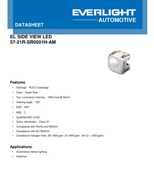
1. Product Overview
This document details the specifications for a high-performance, side-view light-emitting diode (LED) in a PLCC-2 (Plastic Leaded Chip Carrier) surface-mount package. The device emits light in the Super Red spectrum and is engineered for demanding applications, particularly within the automotive sector. Its primary design goals are to provide reliable, consistent illumination in space-constrained environments where a wide viewing angle is essential.
The core advantages of this component include its compact form factor, high luminous output for its package size, and a robust construction that meets stringent automotive-grade reliability standards. It is specifically targeted at markets requiring dependable interior lighting solutions, such as automotive dashboard backlighting, switch illumination, and other indicator functions within vehicle cabins.
2. In-Depth Technical Parameter Analysis
2.1 Photometric and Electrical Characteristics
The key operational parameters define the LED's performance under standard test conditions. The typical forward voltage (VF) is 2.2V when driven at the recommended forward current (IF) of 50mA, with a maximum allowable limit of 70mA. The primary photometric output, luminous intensity (IV), has a typical value of 1900 millicandelas (mcd) at 50mA, with a specified range from 1400mcd (minimum) to 2800mcd (maximum). This high intensity is achieved within a very wide viewing angle (φ) of 120 degrees, defined as the off-axis angle where the luminous intensity drops to half of its peak value. The dominant wavelength (λd) falls within the Super Red band, specified between 627nm and 639nm.
2.2 Thermal and Reliability Characteristics
Thermal management is critical for LED longevity. The device has a thermal resistance from the junction to the solder point (Rth JS) with two values: an electrical measurement of 60 K/W (typical) and a real measurement of 85 K/W (typical). The maximum permissible junction temperature (TJ) is 125°C, while the operating ambient temperature range (Topr) is from -40°C to +110°C. For electrostatic discharge (ESD) protection, the component is rated for 2kV using the Human Body Model (HBM), which is a standard level for industrial components.
2.3 Absolute Maximum Ratings
These ratings define the stress limits beyond which permanent damage may occur. They include a maximum power dissipation (Pd) of 193mW, a maximum forward current (IF) of 70mA, and a surge current (IFM) of 100mA for pulses ≤10μs. The device is not designed for reverse bias operation. The maximum soldering temperature during reflow is specified as 260°C for 30 seconds.
3. Binning System Explanation
To ensure consistency in production, LEDs are sorted into performance bins. This datasheet provides detailed binning information for two key parameters.
3.1 Luminous Intensity Binning
The luminous intensity is categorized into a comprehensive alphanumeric binning structure, ranging from very low output (L1, 11.2-14 mcd) to very high output (GA, 18000-22400 mcd). For this specific product variant, the possible output bins are highlighted, indicating the typical production spread falls within the AA (1120-1400 mcd), AB (1400-1800 mcd), BA (1800-2240 mcd), and BB (2240-2800 mcd) ranges, aligning with the min/typ/max values stated in the characteristics table.
3.2 Dominant Wavelength Binning
The dominant wavelength is also binned using a numeric code system. The bins cover a broad spectrum. For this Super Red LED, the relevant bins are in the 627nm region, corresponding to codes like '2427' (624-627nm) and '273' (the start of the 627nm+ range as per the truncated table). A tolerance of ±1nm is applied to the binned wavelength value.
4. Performance Curve Analysis
The provided graphs offer crucial insights into the LED's behavior under varying conditions.
4.1 IV Curve and Relative Intensity
The Forward Current vs. Forward Voltage graph shows the exponential relationship typical of diodes. The Relative Luminous Intensity vs. Forward Current graph demonstrates that light output increases with current but may exhibit non-linear effects at higher drive levels, emphasizing the importance of constant-current driving.
4.2 Temperature Dependence
The Relative Luminous Intensity vs. Junction Temperature graph shows a negative temperature coefficient; light output decreases as the junction temperature rises. Conversely, the Relative Forward Voltage vs. Junction Temperature graph shows a negative coefficient, where VF decreases with increasing temperature. The wavelength also shifts with temperature, as shown in the Relative Wavelength vs. Junction Temperature graph.
4.3 Spectral Distribution and Derating
The Relative Spectral Distribution graph depicts the narrow emission peak characteristic of a monochromatic LED. The Forward Current Derating Curve is vital for design: it dictates the maximum allowable continuous current based on the temperature measured at the solder pad (TS). For example, at a TS of 110°C, the maximum IF is 55mA. The Permissible Pulse Handling Capability chart defines the surge current limits for different pulse widths and duty cycles.
5. Mechanical and Packaging Information
5.1 Mechanical Dimensions
The component uses a standard PLCC-2 surface-mount package designed for side-view emission. The exact dimensions (length, width, height, lead spacing, etc.) are defined in the mechanical drawing, which is essential for PCB footprint design and ensuring proper fit within the assembly.
5.2 Polarity Identification and Pad Design
The PLCC-2 package has a built-in polarity indicator, typically a notch or a chamfered corner on the package body, which corresponds to the cathode. The recommended soldering pad layout is provided to ensure reliable solder joint formation, proper thermal relief, and mechanical stability during and after the reflow process.
6. Soldering and Assembly Guidelines
6.1 Reflow Soldering Profile
A specific reflow soldering temperature profile is recommended to prevent thermal damage. The profile includes preheat, soak, reflow (with a peak temperature not exceeding 260°C for 30 seconds), and cooling stages. Adhering to this profile is critical for maintaining solder joint integrity and LED reliability.
6.2 Precautions for Use and Storage
General precautions include avoiding mechanical stress on the LED lens, preventing contamination, and using appropriate handling procedures to mitigate ESD risks. Storage conditions should be within the specified temperature and humidity ranges to prevent degradation of the package and leads.
7. Application Recommendations
7.1 Typical Application Scenarios
The primary applications are Automotive interior lighting (e.g., instrument cluster backlighting, infotainment system buttons, ambient lighting) and Switches (illuminated push-buttons, rocker switches). Its side-view emission and wide angle make it ideal for edge-lighting light guides or direct illumination of symbols on a panel.
7.2 Design Considerations
Designers must consider several factors: Current Drive: Use a constant-current driver circuit set to 50mA or lower for optimal performance and lifetime. Thermal Management: Ensure adequate PCB copper pour or thermal vias to dissipate heat from the solder pads, especially when operating at high ambient temperatures or high currents. Optical Design: The 120° viewing angle provides wide coverage but may require light guides or diffusers to achieve uniform illumination over a specific area. Sulfur Resistance: The Class A1 sulfur robustness rating is crucial for automotive environments where atmospheric sulfur can corrode silver-based components, leading to failure.
8. Compliance and Environmental Information
This product is compliant with several important industry standards: RoHS (Restriction of Hazardous Substances): Limits the use of specific hazardous materials. REACH (Registration, Evaluation, Authorisation and Restriction of Chemicals): Compliant with EU regulations. Halogen-Free: Meets strict limits on Bromine (Br) and Chlorine (Cl) content. AEC-Q102: This is a critical qualification for discrete optoelectronic semiconductors in automotive applications, ensuring reliability under automotive stress conditions. Sulfur Robustness Class A1: Indicates a high level of resistance to sulfur-containing atmospheres.
9. Frequently Asked Questions (Based on Technical Parameters)
Q: What is the difference between 'Typ.' and 'Max.' luminous intensity?
A: 'Typ.' (1900mcd) represents the average value from production under test conditions. 'Max.' (2800mcd) is the upper limit of the specified binning range. Individual units will vary within the binned range (e.g., BA, BB).
Q: Can I drive this LED at 70mA continuously?
A: While 70mA is the absolute maximum rating, continuous operation at this level is not recommended. The derating curve must be consulted. At a solder pad temperature of 106°C, the maximum allowed continuous current is only 55mA. For reliable long-term operation, design around the typical 50mA drive current.
Q: Why is the sulfur robustness rating important for automotive use?
A> Automotive cabins and under-hood environments can contain sulfur compounds from materials like rubber and certain lubricants. These compounds can form silver sulfide on LED terminals, increasing resistance and causing failure. The Class A1 rating confirms testing and performance under such conditions.
Q: How do I interpret the binning codes in an order?
A> The part number likely includes codes specifying the luminous intensity bin (e.g., BA) and the dominant wavelength bin (e.g., 273). This allows designers to select the precise performance grade required for their application to ensure color and brightness consistency across multiple units.
10. Operational Principle and Technology Trends
10.1 Basic Operating Principle
A light-emitting diode is a semiconductor p-n junction diode. When a forward voltage is applied, electrons and holes recombine in the active region, releasing energy in the form of photons (light). The wavelength (color) of the emitted light is determined by the bandgap energy of the semiconductor materials used (e.g., AlInGaP for red/orange/yellow). The PLCC package incorporates a reflective cavity and a molded epoxy lens to shape the light output into a wide side-emitting pattern.
10.2 Industry Trends
The trend in such components is towards higher efficiency (more lumens per watt), allowing for lower drive currents and reduced thermal load. Improved color consistency and tighter binning tolerances are critical for applications requiring uniform appearance. Enhanced reliability standards beyond AEC-Q102, such as longer lifetime testing and higher temperature ratings, are being demanded. Integration is another trend, with drivers or multiple LED chips being combined into single modules. Finally, there is a continuous push for miniaturization while maintaining or increasing optical output.
LED Specification Terminology
Complete explanation of LED technical terms
Photoelectric Performance
| Term | Unit/Representation | Simple Explanation | Why Important |
|---|---|---|---|
| Luminous Efficacy | lm/W (lumens per watt) | Light output per watt of electricity, higher means more energy efficient. | Directly determines energy efficiency grade and electricity cost. |
| Luminous Flux | lm (lumens) | Total light emitted by source, commonly called "brightness". | Determines if the light is bright enough. |
| Viewing Angle | ° (degrees), e.g., 120° | Angle where light intensity drops to half, determines beam width. | Affects illumination range and uniformity. |
| CCT (Color Temperature) | K (Kelvin), e.g., 2700K/6500K | Warmth/coolness of light, lower values yellowish/warm, higher whitish/cool. | Determines lighting atmosphere and suitable scenarios. |
| CRI / Ra | Unitless, 0–100 | Ability to render object colors accurately, Ra≥80 is good. | Affects color authenticity, used in high-demand places like malls, museums. |
| SDCM | MacAdam ellipse steps, e.g., "5-step" | Color consistency metric, smaller steps mean more consistent color. | Ensures uniform color across same batch of LEDs. |
| Dominant Wavelength | nm (nanometers), e.g., 620nm (red) | Wavelength corresponding to color of colored LEDs. | Determines hue of red, yellow, green monochrome LEDs. |
| Spectral Distribution | Wavelength vs intensity curve | Shows intensity distribution across wavelengths. | Affects color rendering and quality. |
Electrical Parameters
| Term | Symbol | Simple Explanation | Design Considerations |
|---|---|---|---|
| Forward Voltage | Vf | Minimum voltage to turn on LED, like "starting threshold". | Driver voltage must be ≥Vf, voltages add up for series LEDs. |
| Forward Current | If | Current value for normal LED operation. | Usually constant current drive, current determines brightness & lifespan. |
| Max Pulse Current | Ifp | Peak current tolerable for short periods, used for dimming or flashing. | Pulse width & duty cycle must be strictly controlled to avoid damage. |
| Reverse Voltage | Vr | Max reverse voltage LED can withstand, beyond may cause breakdown. | Circuit must prevent reverse connection or voltage spikes. |
| Thermal Resistance | Rth (°C/W) | Resistance to heat transfer from chip to solder, lower is better. | High thermal resistance requires stronger heat dissipation. |
| ESD Immunity | V (HBM), e.g., 1000V | Ability to withstand electrostatic discharge, higher means less vulnerable. | Anti-static measures needed in production, especially for sensitive LEDs. |
Thermal Management & Reliability
| Term | Key Metric | Simple Explanation | Impact |
|---|---|---|---|
| Junction Temperature | Tj (°C) | Actual operating temperature inside LED chip. | Every 10°C reduction may double lifespan; too high causes light decay, color shift. |
| Lumen Depreciation | L70 / L80 (hours) | Time for brightness to drop to 70% or 80% of initial. | Directly defines LED "service life". |
| Lumen Maintenance | % (e.g., 70%) | Percentage of brightness retained after time. | Indicates brightness retention over long-term use. |
| Color Shift | Δu′v′ or MacAdam ellipse | Degree of color change during use. | Affects color consistency in lighting scenes. |
| Thermal Aging | Material degradation | Deterioration due to long-term high temperature. | May cause brightness drop, color change, or open-circuit failure. |
Packaging & Materials
| Term | Common Types | Simple Explanation | Features & Applications |
|---|---|---|---|
| Package Type | EMC, PPA, Ceramic | Housing material protecting chip, providing optical/thermal interface. | EMC: good heat resistance, low cost; Ceramic: better heat dissipation, longer life. |
| Chip Structure | Front, Flip Chip | Chip electrode arrangement. | Flip chip: better heat dissipation, higher efficacy, for high-power. |
| Phosphor Coating | YAG, Silicate, Nitride | Covers blue chip, converts some to yellow/red, mixes to white. | Different phosphors affect efficacy, CCT, and CRI. |
| Lens/Optics | Flat, Microlens, TIR | Optical structure on surface controlling light distribution. | Determines viewing angle and light distribution curve. |
Quality Control & Binning
| Term | Binning Content | Simple Explanation | Purpose |
|---|---|---|---|
| Luminous Flux Bin | Code e.g., 2G, 2H | Grouped by brightness, each group has min/max lumen values. | Ensures uniform brightness in same batch. |
| Voltage Bin | Code e.g., 6W, 6X | Grouped by forward voltage range. | Facilitates driver matching, improves system efficiency. |
| Color Bin | 5-step MacAdam ellipse | Grouped by color coordinates, ensuring tight range. | Guarantees color consistency, avoids uneven color within fixture. |
| CCT Bin | 2700K, 3000K etc. | Grouped by CCT, each has corresponding coordinate range. | Meets different scene CCT requirements. |
Testing & Certification
| Term | Standard/Test | Simple Explanation | Significance |
|---|---|---|---|
| LM-80 | Lumen maintenance test | Long-term lighting at constant temperature, recording brightness decay. | Used to estimate LED life (with TM-21). |
| TM-21 | Life estimation standard | Estimates life under actual conditions based on LM-80 data. | Provides scientific life prediction. |
| IESNA | Illuminating Engineering Society | Covers optical, electrical, thermal test methods. | Industry-recognized test basis. |
| RoHS / REACH | Environmental certification | Ensures no harmful substances (lead, mercury). | Market access requirement internationally. |
| ENERGY STAR / DLC | Energy efficiency certification | Energy efficiency and performance certification for lighting. | Used in government procurement, subsidy programs, enhances competitiveness. |