1. Product Overview
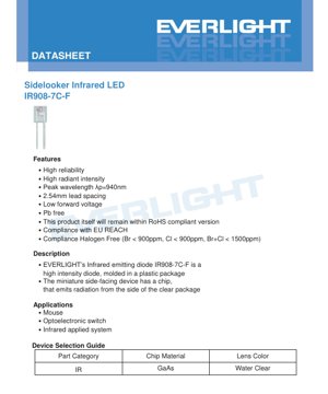
The IR908-7C-F is a high-intensity infrared emitting diode housed in a side-facing plastic package. This design features a chip that emits radiation from the side of the clear epoxy lens, making it suitable for applications requiring a lateral emission profile. The device is characterized by high reliability and radiant intensity, with a peak wavelength of 940nm.
1.1 Core Advantages
- High reliability and radiant intensity.
- Low forward voltage operation.
- Pb-free, RoHS compliant, and compliant with EU REACH and Halogen Free standards (Br < 900ppm, Cl < 900ppm, Br+Cl < 1500ppm).
- Standard 2.54mm lead spacing for easy PCB integration.
1.2 Target Applications
- Computer mice for optical tracking.
- Optoelectronic switches and sensors.
- General infrared application systems.
2. Technical Parameter Deep Dive
2.1 Absolute Maximum Ratings
The following ratings define the limits beyond which permanent damage to the device may occur. All values are specified at an ambient temperature (Ta) of 25°C.
- Continuous Forward Current (IF): 50 mA
- Reverse Voltage (VR): 5 V
- Operating Temperature (Topr): -25 to +85 °C
- Storage Temperature (Tstg): -40 to +85 °C
- Soldering Temperature (Tsol): 260 °C for < 5 seconds
- Power Dissipation (Pd): 75 mW at or below 25°C free air temperature
2.2 Electro-Optical Characteristics
Typical performance parameters are measured at Ta=25°C. The Light Current (IC(ON)) is a key parameter measured under specific test conditions (IF=4mA, VCE=3.5V).
- Peak Wavelength (λp): 940 nm (Typical) at IF=20mA
- Spectral Bandwidth (Δλ): 50 nm (Typical) at IF=20mA
- Forward Voltage (VF): 1.25 V (Typical), 1.60 V (Max) at IF=20mA
- Reverse Current (IR): 10 µA (Max) at VR=5V
- View Angle (2θ1/2): 40 degrees (Typical) at IF=20mA
3. Binning System Explanation
The IR908-7C-F is available in different performance ranks based on its Light Current (IC(ON)). This allows designers to select devices with consistent optical output for their application.
3.1 Detailed Ranks (E1 to E11)
These ranks provide a fine selection of light current. For example, Rank E1 covers 143 to 255 µA, while Rank E11 covers 857 to 1137 µA, all measured at IF=4mA, VCE=3.5V.
3.2 Rough Ranks (7-2, 7-1, 6-2, 6-1)
These are broader categories. For instance, Rank 6-1 covers a light current range from 650 to 1274 µA. It is important to note that this bin table is for reference only and not for specific bin shipment guarantees.
4. Performance Curve Analysis
The datasheet includes several typical characteristic curves that are crucial for circuit design and thermal management.
4.1 Forward Current vs. Ambient Temperature
This curve shows how the maximum allowable forward current decreases as the ambient temperature increases, which is critical for ensuring long-term reliability.
4.2 Spectral Distribution
Illustrates the radiant power output as a function of wavelength, centered around the 940nm peak.
4.3 Forward Current vs. Forward Voltage (IV Curve)
Defines the relationship between the current flowing through the diode and the voltage drop across it, essential for driver circuit design.
4.4 Relative Radiant Intensity vs. Angular Displacement
This polar plot visually represents the 40-degree view angle, showing how the emitted intensity falls off at angles away from the central axis.
5. Mechanical and Package Information
5.1 Package Dimensions
The device comes in a specific side-looking package. All dimensions are in millimeters with a general tolerance of ±0.3mm unless otherwise specified. A detailed dimensioned drawing is provided in the original datasheet, showing the body size, lead length, and spacing.
5.2 Polarity Identification
The anode and cathode are clearly marked. Correct polarity must be observed during circuit assembly to prevent damage.
6. Soldering and Assembly Guidelines
6.1 Lead Forming
- Bending must be performed at a distance greater than 3mm from the bottom of the epoxy resin body.
- The lead frame must be fixed during bending, and stress on the epoxy body must be avoided.
- Lead forming should always be done before the soldering process.
- Cutting of leads should be performed at room temperature.
- PCB holes must align perfectly with the LED leads to avoid mounting stress.
6.2 Soldering Parameters
Care must be taken to keep the solder joint at least 3mm away from the epoxy bulb.
- Hand Soldering: Iron tip temperature max 300°C (30W max), soldering time < 3 seconds.
- Dip Soldering: Preheat temperature max 100°C (<60 sec), solder bath temperature max 260°C for < 5 seconds.
- A recommended soldering temperature profile is provided to minimize thermal shock.
- Avoid mechanical shock or vibration while the LED is hot from soldering.
- Dip or hand soldering should not be performed more than once.
6.3 Cleaning
Ultrasonic cleaning is not recommended for this device.
6.4 Storage Conditions
- After shipment, store at 10-30°C and 70% RH or less for up to 3 months.
- For long-term storage (>3 months to 1 year), use a sealed container with nitrogen atmosphere at 10-25°C and 20-60% RH.
- After opening the original package, use the devices within 24 hours if possible, and store the remainder at 10-25°C and 20-60% RH, resealing the bag promptly.
- Avoid rapid temperature changes in high humidity to prevent condensation.
7. Packaging and Ordering Information
7.1 Packing Specification
The standard packing quantity is 1000 pieces per bag, 8 bags per box, and 10 boxes per carton.
7.2 Label Specification
The product label includes fields for Customer Part Number (CPN), Part Number (P/N), Quantity (QTY), Ranks (CAT), Reference (REF), and Lot Number (LOT No).
8. Application Suggestions and Design Considerations
8.1 Typical Application Circuits
When designing a drive circuit, the low forward voltage (typically 1.25V) allows for operation from low-voltage supplies. A current-limiting resistor is essential to maintain the forward current within the Absolute Maximum Rating of 50mA. For pulsed operation, refer to derating curves not explicitly shown but implied by the power dissipation rating.
8.2 Heat Management
Proper thermal management is critical. The power dissipation is rated at 75mW at 25°C. As the ambient temperature rises, the maximum allowable power and forward current must be derated accordingly. Designers should ensure adequate PCB copper area or other heat sinking methods if operating near maximum ratings or in elevated temperature environments.
8.3 Optical Alignment
The side-emitting nature of this LED requires careful mechanical design to align the emitting surface correctly with the target sensor or optical path. The 40-degree view angle defines the beam spread.
9. Technical Comparison and Differentiation
The primary differentiating factor of the IR908-7C-F is its side-looking (sidelooker) package. Unlike top-emitting LEDs, this package emits infrared light from the side of the component. This is a significant advantage in space-constrained applications like optical computer mice, where the LED and sensor need to be placed parallel to the surface being tracked, or in slot-type opto-interrupters.
10. Frequently Asked Questions (Based on Technical Parameters)
10.1 What is the difference between the E-ranks and the Rough Ranks?
The E-ranks (E1 through E11) offer a finer, more granular selection of light output for applications requiring tight consistency. The Rough Ranks (e.g., 7-2, 6-1) cover wider ranges and are typically used for applications where the exact light current is less critical. The datasheet explicitly states the bin table is for reference only.
10.2 Why is the soldering distance (3mm from epoxy) so important?
The epoxy resin that forms the lens and body of the LED is sensitive to high temperatures. Excessive heat during soldering can cause internal stress, cracking, or degradation of the optical properties, leading to premature failure or reduced light output.
10.3 Can I drive this LED at its maximum continuous current of 50mA?
While possible, it is not recommended for reliable long-term operation, especially at higher ambient temperatures. The power dissipation at 50mA and a typical Vf of 1.25V would be 62.5mW, which is close to the 75mW rating at 25°C. Good heat sinking and current derating according to the Forward Current vs. Ambient Temperature curve are essential for robust design.
11. Practical Design and Usage Case
Case: Integration into an Optoelectronic Switch (Slot Sensor)
In a typical U-shaped slot sensor, the IR908-7C-F is mounted on one side of the slot, facing a phototransistor or photodiode on the opposite side. The side-emitting profile is perfect for this geometry, directing light horizontally across the gap. An object passing through the slot interrupts the beam, triggering the sensor. Design steps include: 1) Selecting an appropriate rank (e.g., E5) for sufficient signal margin. 2) Designing a constant current driver circuit set to 20mA for optimal performance. 3) Ensuring the mechanical housing precisely aligns the LED's emitting side with the receiver. 4) Following all soldering guidelines to prevent damage during PCB assembly.
12. Principle Introduction
Infrared Light Emitting Diodes (IR LEDs) operate on the same fundamental principle as visible LEDs: electroluminescence in a semiconductor material. When a forward voltage is applied across the p-n junction, electrons and holes recombine, releasing energy in the form of photons. The wavelength (color) of the emitted light is determined by the bandgap energy of the semiconductor material. For this device, Gallium Arsenide (GaAs) is used to produce photons in the near-infrared spectrum, specifically at a peak of 940nm, which is invisible to the human eye but easily detected by silicon photodetectors.
13. Development Trends
The trend in infrared LED technology continues towards higher efficiency (more radiant output per electrical watt input), improved reliability, and smaller package sizes. There is also a drive towards specific wavelength optimization for applications like facial recognition (850nm, 940nm) and gas sensing. The side-emitting package style, as seen in the IR908-7C-F, remains a critical form factor for specific optical path designs and is likely to see continued use and refinement in miniaturized sensor modules.
LED Specification Terminology
Complete explanation of LED technical terms
Photoelectric Performance
| Term | Unit/Representation | Simple Explanation | Why Important |
|---|---|---|---|
| Luminous Efficacy | lm/W (lumens per watt) | Light output per watt of electricity, higher means more energy efficient. | Directly determines energy efficiency grade and electricity cost. |
| Luminous Flux | lm (lumens) | Total light emitted by source, commonly called "brightness". | Determines if the light is bright enough. |
| Viewing Angle | ° (degrees), e.g., 120° | Angle where light intensity drops to half, determines beam width. | Affects illumination range and uniformity. |
| CCT (Color Temperature) | K (Kelvin), e.g., 2700K/6500K | Warmth/coolness of light, lower values yellowish/warm, higher whitish/cool. | Determines lighting atmosphere and suitable scenarios. |
| CRI / Ra | Unitless, 0–100 | Ability to render object colors accurately, Ra≥80 is good. | Affects color authenticity, used in high-demand places like malls, museums. |
| SDCM | MacAdam ellipse steps, e.g., "5-step" | Color consistency metric, smaller steps mean more consistent color. | Ensures uniform color across same batch of LEDs. |
| Dominant Wavelength | nm (nanometers), e.g., 620nm (red) | Wavelength corresponding to color of colored LEDs. | Determines hue of red, yellow, green monochrome LEDs. |
| Spectral Distribution | Wavelength vs intensity curve | Shows intensity distribution across wavelengths. | Affects color rendering and quality. |
Electrical Parameters
| Term | Symbol | Simple Explanation | Design Considerations |
|---|---|---|---|
| Forward Voltage | Vf | Minimum voltage to turn on LED, like "starting threshold". | Driver voltage must be ≥Vf, voltages add up for series LEDs. |
| Forward Current | If | Current value for normal LED operation. | Usually constant current drive, current determines brightness & lifespan. |
| Max Pulse Current | Ifp | Peak current tolerable for short periods, used for dimming or flashing. | Pulse width & duty cycle must be strictly controlled to avoid damage. |
| Reverse Voltage | Vr | Max reverse voltage LED can withstand, beyond may cause breakdown. | Circuit must prevent reverse connection or voltage spikes. |
| Thermal Resistance | Rth (°C/W) | Resistance to heat transfer from chip to solder, lower is better. | High thermal resistance requires stronger heat dissipation. |
| ESD Immunity | V (HBM), e.g., 1000V | Ability to withstand electrostatic discharge, higher means less vulnerable. | Anti-static measures needed in production, especially for sensitive LEDs. |
Thermal Management & Reliability
| Term | Key Metric | Simple Explanation | Impact |
|---|---|---|---|
| Junction Temperature | Tj (°C) | Actual operating temperature inside LED chip. | Every 10°C reduction may double lifespan; too high causes light decay, color shift. |
| Lumen Depreciation | L70 / L80 (hours) | Time for brightness to drop to 70% or 80% of initial. | Directly defines LED "service life". |
| Lumen Maintenance | % (e.g., 70%) | Percentage of brightness retained after time. | Indicates brightness retention over long-term use. |
| Color Shift | Δu′v′ or MacAdam ellipse | Degree of color change during use. | Affects color consistency in lighting scenes. |
| Thermal Aging | Material degradation | Deterioration due to long-term high temperature. | May cause brightness drop, color change, or open-circuit failure. |
Packaging & Materials
| Term | Common Types | Simple Explanation | Features & Applications |
|---|---|---|---|
| Package Type | EMC, PPA, Ceramic | Housing material protecting chip, providing optical/thermal interface. | EMC: good heat resistance, low cost; Ceramic: better heat dissipation, longer life. |
| Chip Structure | Front, Flip Chip | Chip electrode arrangement. | Flip chip: better heat dissipation, higher efficacy, for high-power. |
| Phosphor Coating | YAG, Silicate, Nitride | Covers blue chip, converts some to yellow/red, mixes to white. | Different phosphors affect efficacy, CCT, and CRI. |
| Lens/Optics | Flat, Microlens, TIR | Optical structure on surface controlling light distribution. | Determines viewing angle and light distribution curve. |
Quality Control & Binning
| Term | Binning Content | Simple Explanation | Purpose |
|---|---|---|---|
| Luminous Flux Bin | Code e.g., 2G, 2H | Grouped by brightness, each group has min/max lumen values. | Ensures uniform brightness in same batch. |
| Voltage Bin | Code e.g., 6W, 6X | Grouped by forward voltage range. | Facilitates driver matching, improves system efficiency. |
| Color Bin | 5-step MacAdam ellipse | Grouped by color coordinates, ensuring tight range. | Guarantees color consistency, avoids uneven color within fixture. |
| CCT Bin | 2700K, 3000K etc. | Grouped by CCT, each has corresponding coordinate range. | Meets different scene CCT requirements. |
Testing & Certification
| Term | Standard/Test | Simple Explanation | Significance |
|---|---|---|---|
| LM-80 | Lumen maintenance test | Long-term lighting at constant temperature, recording brightness decay. | Used to estimate LED life (with TM-21). |
| TM-21 | Life estimation standard | Estimates life under actual conditions based on LM-80 data. | Provides scientific life prediction. |
| IESNA | Illuminating Engineering Society | Covers optical, electrical, thermal test methods. | Industry-recognized test basis. |
| RoHS / REACH | Environmental certification | Ensures no harmful substances (lead, mercury). | Market access requirement internationally. |
| ENERGY STAR / DLC | Energy efficiency certification | Energy efficiency and performance certification for lighting. | Used in government procurement, subsidy programs, enhances competitiveness. |