Table of Contents
- 1. Product Overview
- 1.1 Core Features and Compliance
- 1.2 Target Applications
- 2. Technical Specifications Deep Dive
- 2.1 Absolute Maximum Ratings
- 2.2 Electro-Optical Characteristics (Ta=25°C)
- 3. Performance Curve Analysis
- 3.1 Implied Curve Information
- 4. Mechanical and Packaging Information
- 4.1 Package Dimensions
- 4.2 Polarity Identification and Mounting
- 5. Soldering and Assembly Guidelines
- 5.1 Storage and Moisture Sensitivity
- 5.2 Soldering Conditions
- 5.3 Rework and Repair
- 6. Packaging and Ordering Information
- 6.1 Tape and Reel Specifications
- 6.2 Label Information
- 7. Application Design Considerations
- 7.1 Circuit Protection
- 7.2 Biasing and Signal Conditioning
- 7.3 Optical Design
- 8. Technical Comparison and Positioning
- 9. Frequently Asked Questions (FAQ)
- 9.1 What is the difference between ISC and IL?
- 9.2 How do I choose the value of the series resistor?
- 9.3 Can this be used for visible light detection?
- 10. Practical Use Case Example
- 11. Operating Principle
- 12. Industry Trends
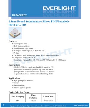
1. Product Overview
The PD42-21C/TR8 is a high-speed, high-sensitivity silicon PIN photodiode designed for infrared detection applications. It is housed in a miniature 1.8mm round, spherical top-view lens surface-mount device (SMD) package molded from black plastic. This compact design makes it suitable for space-constrained applications requiring reliable infrared sensing.
The device is spectrally matched to common infrared emitting diodes, optimizing performance in systems where it is paired with an IR source. Its key advantages include a fast response time, high photosensitivity, and small junction capacitance, which are critical for high-speed signal detection.
1.1 Core Features and Compliance
- Fast Response Time: Enables detection of rapid optical signal changes.
- High Photo Sensitivity: Provides strong electrical output from low light levels.
- Small Junction Capacitance: Contributes to high-speed operation by reducing RC time constants.
- Packaging: Supplied on 12mm tape mounted on a 7-inch diameter reel for automated assembly.
- Environmental Compliance: The product is Pb-free, compliant with RoHS and EU REACH regulations, and is Halogen Free (Br<900 ppm, Cl<900 ppm, Br+Cl<1500 ppm).
1.2 Target Applications
This photodiode is engineered for use in various electronic systems requiring precise infrared detection.
- High-speed photo detectors
- Photocopiers
- Game machines and interactive devices
- General infrared application systems (e.g., proximity sensors, data transmission)
2. Technical Specifications Deep Dive
2.1 Absolute Maximum Ratings
Operating the device beyond these limits may cause permanent damage.
- Reverse Voltage (VR): 32 V
- Operating Temperature (Topr): -25°C to +85°C
- Storage Temperature (Tstg): -40°C to +85°C
- Soldering Temperature (Tsol): 260°C for ≤5 seconds
- Power Dissipation (Pd): 150 mW at or below 25°C free air temperature
2.2 Electro-Optical Characteristics (Ta=25°C)
These parameters define the photodiode's performance under typical conditions.
- Spectral Bandwidth (λ0.5): 730 nm to 1100 nm. The device is sensitive across the near-infrared spectrum.
- Peak Sensitivity Wavelength (λP): 940 nm. Maximum responsivity occurs at this infrared wavelength.
- Open-Circuit Voltage (VOC): Typically 0.42 V when illuminated with 5 mW/cm² at 940nm.
- Short-Circuit Current (ISC): 2.0 to 12 μA (Typ. 5.0 μA) when illuminated with 1 mW/cm² at 875nm.
- Reverse Light Current (IL): 2.0 to 12 μA (Typ. 5.0 μA) at VR=5V when illuminated with 1 mW/cm² at 875nm. This is the primary operating parameter in photoconductive mode.
- Dark Current (ID): Maximum 10 nA at VR=10V. This is the leakage current in the absence of light.
- Reverse Breakdown Voltage (VBR): Minimum 32 V, Typical 170 V at IR=100μA.
- Total Capacitance (Ct): Typically 5 pF at VR=5V, f=1MHz. Low capacitance is key for high bandwidth.
- Rise/Fall Time (tr, tf): Typically 6 ns each at VR=10V, RL=1kΩ. This specifies the speed of the electrical response to a light pulse.
3. Performance Curve Analysis
The datasheet includes typical characteristic curves which are essential for design engineers. While specific graphical data is not provided in text form, these curves typically illustrate the relationship between key parameters, helping to predict device behavior under non-standard conditions.
3.1 Implied Curve Information
Based on standard photodiode characteristics, the following relationships are typically plotted:
- Spectral Response: A curve showing relative responsivity versus wavelength, peaking at 940 nm and dropping to half at 730 nm and 1100 nm.
- Current vs. Illuminance (IL vs. Ee): Expected to be linear over a wide range, confirming the photodiode's suitability for analog light measurement.
- Capacitance vs. Reverse Voltage (Ct vs. VR): Capacitance typically decreases with increasing reverse bias, affecting frequency response.
- Dark Current vs. Temperature (ID vs. T): Dark current approximately doubles for every 10°C rise in temperature, which is critical for high-temperature operation.
4. Mechanical and Packaging Information
4.1 Package Dimensions
The photodiode comes in a subminiature round package with a 1.8mm body diameter. Detailed mechanical drawings in the datasheet specify all critical dimensions including lens height, lead spacing, and overall footprint. Tolerances are typically ±0.1mm unless otherwise noted. A suggested pad layout is provided for PCB design reference, but engineers are advised to modify it based on their specific assembly process and thermal requirements.
4.2 Polarity Identification and Mounting
The SMD package has a specific orientation. The datasheet drawing indicates the cathode and anode terminals. Correct polarity is crucial for proper circuit operation. The black plastic body with a clear spherical lens aids in directional sensitivity.
5. Soldering and Assembly Guidelines
Proper handling is vital to maintain device reliability and performance.
5.1 Storage and Moisture Sensitivity
- Do not open the moisture-proof bag until ready for use.
- Store unopened bags at 10°C~30°C and ≤90% RH.
- Use within one year of shipment.
- After opening, devices must be used within 168 hours (floor life) when stored at 10°C~30°C and ≤60% RH. Otherwise, they must be rebaked and stored in a dry bag.
- Baking procedure: 96 hours at 60°C ± 5°C and <5% RH.
5.2 Soldering Conditions
- Reflow Soldering: A recommended temperature profile is provided. Do not exceed two reflow cycles.
- Hand Soldering: Use a soldering iron with a tip temperature <350°C and power <25W. Contact time per terminal should be <3 seconds. Allow a 2-second interval between soldering each terminal to prevent thermal damage.
- Avoid mechanical stress on the device during heating and avoid warping the PCB after soldering.
5.3 Rework and Repair
Repair after soldering is not recommended. If unavoidable, use a double-head soldering iron to simultaneously heat both terminals and lift the component evenly. Always verify device functionality after any rework.
6. Packaging and Ordering Information
6.1 Tape and Reel Specifications
The device is packaged in carrier tape with dimensions specified in the datasheet. Standard quantity is 1000 pieces per 7-inch reel. The tape dimensions ensure compatibility with standard SMD pick-and-place equipment.
6.2 Label Information
The reel label contains standard information for traceability and correct assembly: Customer Part Number (CPN), Part Number (P/N), Lot Number, Quantity, Peak Wavelength (HUE), Ranks (CAT), Reference (REF), Moisture Sensitivity Level (MSL-X), and Manufacture Origin.
7. Application Design Considerations
7.1 Circuit Protection
Critical: An external current-limiting resistor must be used in series with the photodiode when operating in photoconductive mode (reverse-biased). Without it, a small voltage change can cause a large current surge, potentially burning out the device.
7.2 Biasing and Signal Conditioning
The photodiode can be used in two primary modes:
- Photovoltaic Mode (Zero Bias): Generates a voltage (VOC). Offers low noise but slower response.
- Photoconductive Mode (Reverse Bias): Operated with a reverse voltage (e.g., 5V as in specs). This reduces junction capacitance (speeding up response) and improves linearity but increases dark current. A transimpedance amplifier (TIA) is commonly used to convert the photocurrent (IL) into a usable voltage signal.
7.3 Optical Design
The spherical lens has a specific viewing angle. For optimal coupling, align the IR source within this angle. The black housing minimizes internal reflections and crosstalk from ambient light.
8. Technical Comparison and Positioning
Compared to standard photodiodes, the PD42-21C/TR8 offers a balance of speed (6 ns), sensitivity (5 μA typical at 1mW/cm²), and a very compact SMD footprint. Its 940nm peak sensitivity makes it a direct match for many low-cost IR LEDs. The low capacitance is a key differentiator for high-frequency applications compared to devices with larger active areas.
9. Frequently Asked Questions (FAQ)
9.1 What is the difference between ISC and IL?
ISC (Short-Circuit Current) is measured with zero voltage across the diode. IL (Reverse Light Current) is measured under an applied reverse bias (e.g., 5V). In a well-designed PIN photodiode, these values are very similar, as shown in the datasheet (both Typ. 5.0 μA). IL is the more practical parameter for circuit design in biased operation.
9.2 How do I choose the value of the series resistor?
The resistor limits the current under maximum illumination. Calculate R ≥ (Supply Voltage) / (Maximum IL). From specs, Max IL is 12 μA. For a 5V bias, R should be ≥ 5V / 12μA ≈ 417 kΩ. A common starting value is 100 kΩ, which also sets the bandwidth in conjunction with the junction capacitance.
9.3 Can this be used for visible light detection?
Its spectral range starts at 730 nm, which is in the near-infrared. It has very low sensitivity to visible light (wavelengths below 700 nm). For visible light, a photodiode with a peak sensitivity in the 550-650 nm range would be more appropriate.
10. Practical Use Case Example
Scenario: Infrared Proximity Sensor in a Game Controller.
- Component Pairing: The PD42-21C/TR8 is paired with a 940nm IR LED.
- Circuit Design: The photodiode is reverse-biased with 3.3V through a 100 kΩ resistor. Its output is connected to the inverting input of an op-amp configured as a TIA with a 1 MΩ feedback resistor and a small feedback capacitor (e.g., 1 pF) to stabilize the response.
- Operation: The IR LED emits a pulsed signal. When an object (e.g., a user's hand) comes near, it reflects IR light to the photodiode. The TIA converts the increased photocurrent into a measurable voltage spike.
- Benefits: The photodiode's fast response allows for quick detection of rapid hand movements. Its small size fits easily into the compact controller housing. The high sensitivity ensures reliable operation even with weak reflected signals.
11. Operating Principle
A PIN photodiode consists of a wide, lightly doped intrinsic (I) region sandwiched between P-type and N-type semiconductor regions. When reverse-biased, the intrinsic region becomes fully depleted, creating a large electric field. Incident photons with energy greater than the semiconductor's bandgap are absorbed, creating electron-hole pairs. The strong electric field swiftly separates these carriers, generating a photocurrent that is proportional to the light intensity. The wide intrinsic region reduces junction capacitance (enabling high speed) and increases the volume for photon absorption (improving sensitivity), compared to a standard PN photodiode.
12. Industry Trends
The demand for miniature, high-speed photodetectors continues to grow, driven by applications in consumer electronics (smartphones, wearables), automotive (LiDAR, in-cabin sensing), and industrial automation. Trends include further miniaturization, integration of photodiodes with amplification and digitization circuits on a single chip (e.g., integrated optical sensors), and enhanced performance in specific wavelength bands for emerging applications like gesture recognition and 3D sensing. Devices like the PD42-21C/TR8 represent a mature, reliable solution for cost-sensitive, high-volume applications requiring robust infrared detection.
LED Specification Terminology
Complete explanation of LED technical terms
Photoelectric Performance
| Term | Unit/Representation | Simple Explanation | Why Important |
|---|---|---|---|
| Luminous Efficacy | lm/W (lumens per watt) | Light output per watt of electricity, higher means more energy efficient. | Directly determines energy efficiency grade and electricity cost. |
| Luminous Flux | lm (lumens) | Total light emitted by source, commonly called "brightness". | Determines if the light is bright enough. |
| Viewing Angle | ° (degrees), e.g., 120° | Angle where light intensity drops to half, determines beam width. | Affects illumination range and uniformity. |
| CCT (Color Temperature) | K (Kelvin), e.g., 2700K/6500K | Warmth/coolness of light, lower values yellowish/warm, higher whitish/cool. | Determines lighting atmosphere and suitable scenarios. |
| CRI / Ra | Unitless, 0–100 | Ability to render object colors accurately, Ra≥80 is good. | Affects color authenticity, used in high-demand places like malls, museums. |
| SDCM | MacAdam ellipse steps, e.g., "5-step" | Color consistency metric, smaller steps mean more consistent color. | Ensures uniform color across same batch of LEDs. |
| Dominant Wavelength | nm (nanometers), e.g., 620nm (red) | Wavelength corresponding to color of colored LEDs. | Determines hue of red, yellow, green monochrome LEDs. |
| Spectral Distribution | Wavelength vs intensity curve | Shows intensity distribution across wavelengths. | Affects color rendering and quality. |
Electrical Parameters
| Term | Symbol | Simple Explanation | Design Considerations |
|---|---|---|---|
| Forward Voltage | Vf | Minimum voltage to turn on LED, like "starting threshold". | Driver voltage must be ≥Vf, voltages add up for series LEDs. |
| Forward Current | If | Current value for normal LED operation. | Usually constant current drive, current determines brightness & lifespan. |
| Max Pulse Current | Ifp | Peak current tolerable for short periods, used for dimming or flashing. | Pulse width & duty cycle must be strictly controlled to avoid damage. |
| Reverse Voltage | Vr | Max reverse voltage LED can withstand, beyond may cause breakdown. | Circuit must prevent reverse connection or voltage spikes. |
| Thermal Resistance | Rth (°C/W) | Resistance to heat transfer from chip to solder, lower is better. | High thermal resistance requires stronger heat dissipation. |
| ESD Immunity | V (HBM), e.g., 1000V | Ability to withstand electrostatic discharge, higher means less vulnerable. | Anti-static measures needed in production, especially for sensitive LEDs. |
Thermal Management & Reliability
| Term | Key Metric | Simple Explanation | Impact |
|---|---|---|---|
| Junction Temperature | Tj (°C) | Actual operating temperature inside LED chip. | Every 10°C reduction may double lifespan; too high causes light decay, color shift. |
| Lumen Depreciation | L70 / L80 (hours) | Time for brightness to drop to 70% or 80% of initial. | Directly defines LED "service life". |
| Lumen Maintenance | % (e.g., 70%) | Percentage of brightness retained after time. | Indicates brightness retention over long-term use. |
| Color Shift | Δu′v′ or MacAdam ellipse | Degree of color change during use. | Affects color consistency in lighting scenes. |
| Thermal Aging | Material degradation | Deterioration due to long-term high temperature. | May cause brightness drop, color change, or open-circuit failure. |
Packaging & Materials
| Term | Common Types | Simple Explanation | Features & Applications |
|---|---|---|---|
| Package Type | EMC, PPA, Ceramic | Housing material protecting chip, providing optical/thermal interface. | EMC: good heat resistance, low cost; Ceramic: better heat dissipation, longer life. |
| Chip Structure | Front, Flip Chip | Chip electrode arrangement. | Flip chip: better heat dissipation, higher efficacy, for high-power. |
| Phosphor Coating | YAG, Silicate, Nitride | Covers blue chip, converts some to yellow/red, mixes to white. | Different phosphors affect efficacy, CCT, and CRI. |
| Lens/Optics | Flat, Microlens, TIR | Optical structure on surface controlling light distribution. | Determines viewing angle and light distribution curve. |
Quality Control & Binning
| Term | Binning Content | Simple Explanation | Purpose |
|---|---|---|---|
| Luminous Flux Bin | Code e.g., 2G, 2H | Grouped by brightness, each group has min/max lumen values. | Ensures uniform brightness in same batch. |
| Voltage Bin | Code e.g., 6W, 6X | Grouped by forward voltage range. | Facilitates driver matching, improves system efficiency. |
| Color Bin | 5-step MacAdam ellipse | Grouped by color coordinates, ensuring tight range. | Guarantees color consistency, avoids uneven color within fixture. |
| CCT Bin | 2700K, 3000K etc. | Grouped by CCT, each has corresponding coordinate range. | Meets different scene CCT requirements. |
Testing & Certification
| Term | Standard/Test | Simple Explanation | Significance |
|---|---|---|---|
| LM-80 | Lumen maintenance test | Long-term lighting at constant temperature, recording brightness decay. | Used to estimate LED life (with TM-21). |
| TM-21 | Life estimation standard | Estimates life under actual conditions based on LM-80 data. | Provides scientific life prediction. |
| IESNA | Illuminating Engineering Society | Covers optical, electrical, thermal test methods. | Industry-recognized test basis. |
| RoHS / REACH | Environmental certification | Ensures no harmful substances (lead, mercury). | Market access requirement internationally. |
| ENERGY STAR / DLC | Energy efficiency certification | Energy efficiency and performance certification for lighting. | Used in government procurement, subsidy programs, enhances competitiveness. |