Table of Contents
- 1. Product Overview
- 2. In-Depth Technical Parameter Analysis
- 2.1 Absolute Maximum Ratings
- 2.2 Electro-Optical Characteristics
- 3. Performance Curve Analysis
- 4. Mechanical and Packaging Information
- 4.1 Package Dimension
- 4.2 Polarity Identification
- 5. Soldering and Assembly Guidelines
- 6. Packaging and Ordering Information
- 7. Application Suggestions
- 7.1 Typical Application Scenarios
- 7.2 Design Considerations
- 8. Technical Comparison and Differentiation
- 9. Frequently Asked Questions (Based on Technical Parameters)
- 10. Practical Design and Usage Examples
- 11. Principle of Operation Introduction
- 12. Technology Trends and Context
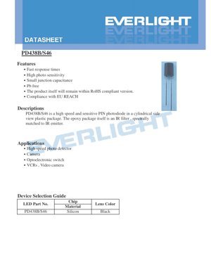
1. Product Overview
The PD438B/S46 is a high-performance silicon PIN photodiode designed for applications requiring fast response and high sensitivity. It is housed in a compact, cylindrical side-view plastic package with a 4.8mm semi-lens. A key feature of this device is its epoxy package, which is formulated to act as an integrated infrared (IR) filter. This filter is spectrally matched to common IR emitters, enhancing its performance in IR sensing applications by reducing sensitivity to unwanted visible light.
The core advantages of this photodiode include its fast response times, which are critical for high-speed data transmission and switching applications, and its high photosensitivity, allowing it to detect low light levels effectively. Its small junction capacitance contributes to the fast response and makes it suitable for high-frequency circuits. The device is constructed using lead-free materials and complies with relevant environmental regulations such as RoHS and EU REACH, making it suitable for use in products with strict environmental compliance requirements.
The primary target markets and applications for the PD438B/S46 are in consumer electronics, industrial automation, and communication systems. Its specifications make it an ideal component for designers working on high-speed optical data links, presence detection systems, and precision light measurement equipment.
2. In-Depth Technical Parameter Analysis
2.1 Absolute Maximum Ratings
The device is rated to withstand a maximum reverse voltage (VR) of 32V. The maximum power dissipation (Pd) is 150 mW, which defines the thermal limits of operation. The leads can be soldered at a temperature up to 260°C for a duration not exceeding 5 seconds, which is compatible with standard reflow soldering processes. The operational temperature range is specified from -40°C to +85°C, and it can be stored in environments ranging from -40°C to +100°C. These ratings ensure reliable performance in a wide variety of environmental conditions.
2.2 Electro-Optical Characteristics
The photodiode's spectral response is defined by its range of spectral bandwidth (λ0.5), which spans from 840 nm to 1100 nm. The peak sensitivity wavelength (λp) is at 940 nm, placing it squarely in the near-infrared region, which is commonly used for remote controls, optical sensors, and free-space communication.
Under an irradiance of 5 mW/cm² at 940 nm, the typical open-circuit voltage (VOC) is 0.35V. The short-circuit current (ISC), measured at 1 mW/cm² and 940 nm, is typically 18 µA. This parameter is a direct measure of the device's current-generating capability under illumination.
The reverse light current (IL) is the photocurrent generated when the diode is reverse-biased. At VR=5V and Ee=1 mW/cm² (λp=940nm), the typical value is 18 µA, with a minimum guaranteed value of 10.2 µA. The dark current (Id), which is the leakage current under no illumination at VR=10V, is typically 5 nA with a maximum of 30 nA. A low dark current is essential for achieving a good signal-to-noise ratio, especially in low-light detection scenarios.
The reverse breakdown voltage (BVR) is specified at a minimum of 32V when a current of 100 µA flows, with a typical value as high as 170V. The total terminal capacitance (Ct) at VR=5V and 1 MHz is typically 18 pF. This low capacitance is a key factor enabling the fast rise and fall times. The rise and fall times (tr/tf) are both typically 50 nanoseconds when the device is operated at VR=10V with a load resistance (RL) of 1 kΩ.
3. Performance Curve Analysis
The datasheet provides several characteristic curves that offer deeper insight into the device's behavior under varying conditions.
Figure 1: Power Dissipation vs. Ambient Temperature illustrates the derating of the maximum allowable power dissipation as the ambient temperature increases. This graph is crucial for thermal management design to prevent overheating and ensure long-term reliability.
Figure 2: Spectral Sensitivity shows the relative responsivity of the photodiode across the wavelength spectrum from approximately 600 nm to 1200 nm. The curve peaks at 940 nm and shows the effective filtering action of the epoxy package, which attenuates response outside the target IR band.
Figure 3: Dark Current vs. Ambient Temperature demonstrates how the leakage current (Id) increases exponentially with temperature. This relationship is vital for applications operating at elevated temperatures, as it defines the noise floor of the sensor.
Figure 4: Reverse Light Current vs. Irradiance (Ee) depicts the linear relationship between the generated photocurrent and the incident light power density. This linearity is a fundamental property of PIN photodiodes and is essential for analog light measurement applications.
Figure 5: Terminal Capacitance vs. Reverse Voltage shows that the junction capacitance decreases with increasing reverse bias voltage. Designers can use this relationship to optimize the speed of their circuit by selecting an appropriate bias point.
Figure 6: Response Time vs. Load Resistance indicates how the rise/fall time of the photodiode's output signal is affected by the load resistance connected to it. Faster response is achieved with lower load resistances, though this may trade off against output voltage swing.
4. Mechanical and Packaging Information
4.1 Package Dimension
The PD438B/S46 comes in a cylindrical side-view package. The key dimensions include a body diameter and a semi-lens height as defined in the package drawing. All unspecified tolerances for linear dimensions are ±0.25mm. The package is colored black, which helps in reducing stray light interference. The side-view configuration allows for sensing light from a direction parallel to the PCB plane, which is useful in applications like paper detection in printers or edge sensing.
4.2 Polarity Identification
The cathode is typically identified by a longer lead, a notch, or a flat spot on the package body. Correct polarity must be observed during assembly, as reverse biasing is the standard operating condition for photodiodes used in photoconductive mode.
5. Soldering and Assembly Guidelines
The device is suitable for wave soldering and reflow soldering processes. The absolute maximum rating for lead soldering temperature is 260°C, with a note that the soldering time should not exceed 5 seconds. It is recommended to follow standard IPC guidelines for soldering electronic components. The device should be stored in a dry, anti-static environment within its specified storage temperature range of -40°C to +100°C to prevent moisture absorption and electrostatic damage.
6. Packaging and Ordering Information
The standard packing specification is as follows: 200 to 500 pieces are packed in one moisture barrier bag. Six such bags are placed into one inner carton. Ten inner cartons are then packed into one master shipping carton. The label on the packaging includes fields for the customer's part number (CPN), the manufacturer's part number (P/N), packing quantity (QTY), and lot number (LOT No.). Other fields like CAT, HUE, and REF, which are common for LEDs to denote intensity, wavelength, and voltage bins, are not applicable for this photodiode as it is not binned in the same way; these fields may be left blank or used for other traceability information.
7. Application Suggestions
7.1 Typical Application Scenarios
- High-Speed Photo Detection: Ideal for optical encoders, data communication over plastic optical fiber (POF), and laser beam detection where nanosecond response is required.
- Camera Applications: Can be used for ambient light sensing (ALS) or IR proximity detection in smartphones, tablets, and digital cameras. The built-in IR filter helps in accurately measuring IR levels.
- Optoelectronic Switches: Suitable for object detection, counting, and position sensing in vending machines, industrial automation, and security systems.
- Consumer Electronics: Used in VCRs and video cameras for tape-end detection or control signal reception.
7.2 Design Considerations
When designing a circuit with the PD438B/S46, consider the following:
- Bias Voltage: A reverse bias voltage (typically 5V to 10V as per datasheet conditions) is applied to widen the depletion region, reducing capacitance and improving speed. Ensure the voltage does not exceed the maximum rating of 32V.
- Load Resistor (RL): The value of RL in the transimpedance configuration directly affects bandwidth and output voltage. A smaller RL gives faster response but lower output signal. Figure 6 in the datasheet is a key reference.
- Amplification: The photocurrent is small (microamps). A transimpedance amplifier (TIA) is almost always used to convert this current into a usable voltage signal. Choose an op-amp with low input bias current and sufficient bandwidth.
- Noise Reduction: Shield the photodiode and its connecting traces from electrical noise. Use a bypass capacitor close to the device's power pins if an active bias circuit is used. The low dark current helps maintain a good signal-to-noise ratio.
- Optical Considerations: Ensure the lens is clean and unobstructed. The side-view package may require careful mechanical design to align the light path correctly.
8. Technical Comparison and Differentiation
Compared to standard PN photodiodes, the PIN structure of the PD438B/S46 offers distinct advantages. The intrinsic (I) region between the P and N layers creates a larger depletion region. This results in two primary benefits: 1) Lower Junction Capacitance: The larger depletion region acts like a wider dielectric, significantly reducing capacitance (typically 18 pF), which is the main enabler for high-speed operation. 2) Improved Linearity and Sensitivity: The wide intrinsic region allows more efficient collection of photogenerated carriers across a broader volume, leading to better linearity in photocurrent vs. irradiance and potentially higher quantum efficiency at its peak wavelength.
Furthermore, the integration of an IR-filtering epoxy directly into the package is a differentiating feature. It eliminates the need for a separate external IR filter, saving space, reducing cost, and simplifying assembly. This makes it particularly advantageous for compact consumer electronics designs.
9. Frequently Asked Questions (Based on Technical Parameters)
Q: What is the difference between short-circuit current (ISC) and reverse light current (IL)?
A: ISC is measured with zero volts across the diode (short-circuit condition). IL is measured when the diode is reverse-biased (e.g., at VR=5V). In practice, for a PIN photodiode, these values are very similar because the photocurrent is largely independent of the reverse bias voltage in the normal operating range.
Q: Why is the rise/fall time specified with a 1 kΩ load?
A: The 1 kΩ load represents a common load condition for testing and for simple circuits. The actual response time in your application will depend on your specific circuit's load resistance and parasitic capacitances, as shown in Figure 6.
Q: Can this photodiode be used for visible light detection?
A: While the silicon material itself is sensitive to visible light (as seen in the spectral curve extending down to ~600nm), the black epoxy package acts as a strong filter. Its sensitivity in the visible spectrum will be greatly attenuated compared to its peak at 940 nm. It is primarily designed for near-IR applications.
Q: How do I interpret the "Typ." values in the characteristics table?
A> "Typ." stands for typical value, which is the expected average under specified conditions. It is not guaranteed. For design purposes, especially for critical parameters, you should use the "Min." or "Max." values to ensure your circuit will function correctly across all production variations and conditions.
10. Practical Design and Usage Examples
Example 1: Simple Object Detection Switch
A basic opto-switch can be built by pairing the PD438B/S46 with an IR LED (e.g., emitting at 940 nm). The photodiode is connected in reverse bias with a pull-up resistor to Vcc (e.g., 5V). The output node between the resistor and the photodiode's cathode is fed to a comparator or a microcontroller's digital input pin. When an object interrupts the IR beam between the LED and the photodiode, the photocurrent drops, causing the voltage at the output node to rise, triggering the detection signal. The fast response time allows detection of rapidly moving objects.
Example 2: Ambient Light Sensor with Microcontroller
For analog light level measurement, the photodiode can be connected to a transimpedance amplifier. The output voltage of the TIA, which is proportional to the incident IR light intensity, is then fed into an analog-to-digital converter (ADC) input of a microcontroller. The MCU can use this reading to automatically adjust the brightness of a display or to determine if an IR remote control signal is present. The integrated IR filter helps ensure the reading is specific to the IR component of ambient light.
11. Principle of Operation Introduction
A PIN photodiode is a semiconductor device that converts light into electrical current. It consists of a layer of intrinsic (undoped or lightly doped) semiconductor material (the "I" region) sandwiched between a P-type layer and an N-type layer. When photons with energy greater than the semiconductor's bandgap (for silicon, light with wavelength less than ~1100 nm) strike the device, they can create electron-hole pairs in the intrinsic region. When a reverse bias voltage is applied, it creates a strong electric field across the intrinsic region. This field swiftly sweeps the photogenerated carriers towards the respective terminals—electrons to the N-side and holes to the P-side—generating a measurable photocurrent in the external circuit. The width of the intrinsic region is key: it allows efficient carrier generation and collection while keeping the device capacitance low.
12. Technology Trends and Context
Silicon PIN photodiodes like the PD438B/S46 represent a mature and highly reliable technology. Current trends in this field focus on several areas: Miniaturization: Developing smaller package footprints (e.g., chip-scale packages) for space-constrained applications like wearable devices and mobile phones. Integration: Combining the photodiode with amplification, digitization, and signal processing circuitry on a single chip to create smart optical sensors. Enhanced Performance: Research into structures like avalanche photodiodes (APDs) for applications requiring extreme sensitivity, though these are more complex and expensive. New Materials: Exploration of materials like germanium or III-V compounds (e.g., InGaAs) for detection in longer infrared wavelengths, which are not accessible with standard silicon. For mainstream near-IR applications up to 1100 nm, silicon remains the dominant, cost-effective material of choice due to its excellent manufacturability and performance.
LED Specification Terminology
Complete explanation of LED technical terms
Photoelectric Performance
| Term | Unit/Representation | Simple Explanation | Why Important |
|---|---|---|---|
| Luminous Efficacy | lm/W (lumens per watt) | Light output per watt of electricity, higher means more energy efficient. | Directly determines energy efficiency grade and electricity cost. |
| Luminous Flux | lm (lumens) | Total light emitted by source, commonly called "brightness". | Determines if the light is bright enough. |
| Viewing Angle | ° (degrees), e.g., 120° | Angle where light intensity drops to half, determines beam width. | Affects illumination range and uniformity. |
| CCT (Color Temperature) | K (Kelvin), e.g., 2700K/6500K | Warmth/coolness of light, lower values yellowish/warm, higher whitish/cool. | Determines lighting atmosphere and suitable scenarios. |
| CRI / Ra | Unitless, 0–100 | Ability to render object colors accurately, Ra≥80 is good. | Affects color authenticity, used in high-demand places like malls, museums. |
| SDCM | MacAdam ellipse steps, e.g., "5-step" | Color consistency metric, smaller steps mean more consistent color. | Ensures uniform color across same batch of LEDs. |
| Dominant Wavelength | nm (nanometers), e.g., 620nm (red) | Wavelength corresponding to color of colored LEDs. | Determines hue of red, yellow, green monochrome LEDs. |
| Spectral Distribution | Wavelength vs intensity curve | Shows intensity distribution across wavelengths. | Affects color rendering and quality. |
Electrical Parameters
| Term | Symbol | Simple Explanation | Design Considerations |
|---|---|---|---|
| Forward Voltage | Vf | Minimum voltage to turn on LED, like "starting threshold". | Driver voltage must be ≥Vf, voltages add up for series LEDs. |
| Forward Current | If | Current value for normal LED operation. | Usually constant current drive, current determines brightness & lifespan. |
| Max Pulse Current | Ifp | Peak current tolerable for short periods, used for dimming or flashing. | Pulse width & duty cycle must be strictly controlled to avoid damage. |
| Reverse Voltage | Vr | Max reverse voltage LED can withstand, beyond may cause breakdown. | Circuit must prevent reverse connection or voltage spikes. |
| Thermal Resistance | Rth (°C/W) | Resistance to heat transfer from chip to solder, lower is better. | High thermal resistance requires stronger heat dissipation. |
| ESD Immunity | V (HBM), e.g., 1000V | Ability to withstand electrostatic discharge, higher means less vulnerable. | Anti-static measures needed in production, especially for sensitive LEDs. |
Thermal Management & Reliability
| Term | Key Metric | Simple Explanation | Impact |
|---|---|---|---|
| Junction Temperature | Tj (°C) | Actual operating temperature inside LED chip. | Every 10°C reduction may double lifespan; too high causes light decay, color shift. |
| Lumen Depreciation | L70 / L80 (hours) | Time for brightness to drop to 70% or 80% of initial. | Directly defines LED "service life". |
| Lumen Maintenance | % (e.g., 70%) | Percentage of brightness retained after time. | Indicates brightness retention over long-term use. |
| Color Shift | Δu′v′ or MacAdam ellipse | Degree of color change during use. | Affects color consistency in lighting scenes. |
| Thermal Aging | Material degradation | Deterioration due to long-term high temperature. | May cause brightness drop, color change, or open-circuit failure. |
Packaging & Materials
| Term | Common Types | Simple Explanation | Features & Applications |
|---|---|---|---|
| Package Type | EMC, PPA, Ceramic | Housing material protecting chip, providing optical/thermal interface. | EMC: good heat resistance, low cost; Ceramic: better heat dissipation, longer life. |
| Chip Structure | Front, Flip Chip | Chip electrode arrangement. | Flip chip: better heat dissipation, higher efficacy, for high-power. |
| Phosphor Coating | YAG, Silicate, Nitride | Covers blue chip, converts some to yellow/red, mixes to white. | Different phosphors affect efficacy, CCT, and CRI. |
| Lens/Optics | Flat, Microlens, TIR | Optical structure on surface controlling light distribution. | Determines viewing angle and light distribution curve. |
Quality Control & Binning
| Term | Binning Content | Simple Explanation | Purpose |
|---|---|---|---|
| Luminous Flux Bin | Code e.g., 2G, 2H | Grouped by brightness, each group has min/max lumen values. | Ensures uniform brightness in same batch. |
| Voltage Bin | Code e.g., 6W, 6X | Grouped by forward voltage range. | Facilitates driver matching, improves system efficiency. |
| Color Bin | 5-step MacAdam ellipse | Grouped by color coordinates, ensuring tight range. | Guarantees color consistency, avoids uneven color within fixture. |
| CCT Bin | 2700K, 3000K etc. | Grouped by CCT, each has corresponding coordinate range. | Meets different scene CCT requirements. |
Testing & Certification
| Term | Standard/Test | Simple Explanation | Significance |
|---|---|---|---|
| LM-80 | Lumen maintenance test | Long-term lighting at constant temperature, recording brightness decay. | Used to estimate LED life (with TM-21). |
| TM-21 | Life estimation standard | Estimates life under actual conditions based on LM-80 data. | Provides scientific life prediction. |
| IESNA | Illuminating Engineering Society | Covers optical, electrical, thermal test methods. | Industry-recognized test basis. |
| RoHS / REACH | Environmental certification | Ensures no harmful substances (lead, mercury). | Market access requirement internationally. |
| ENERGY STAR / DLC | Energy efficiency certification | Energy efficiency and performance certification for lighting. | Used in government procurement, subsidy programs, enhances competitiveness. |