Table of Contents
- 1. Product Overview
- 2. In-Depth Technical Parameter Analysis
- 2.1 Absolute Maximum Ratings
- 2.2 Electro-Optical Characteristics (Ta=25°C)
- 3. Performance Curve Analysis
- 4. Mechanical and Package Information
- 4.1 Package Dimensions
- 4.2 Polarity Identification
- 5. Soldering and Assembly Guidelines
- 5.1 Storage and Moisture Sensitivity
- 5.2 Soldering Conditions
- 6. Packaging and Ordering Information
- 7. Application Notes and Design Considerations
- 7.1 Typical Application Circuits
- 7.2 Critical Design Precautions
- 8. Technical Comparison and Differentiation
- 9. Frequently Asked Questions (FAQs)
- 10. Operational Principle
- 11. Industry Trends
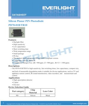
1. Product Overview
The PD70-01B/TR10 is a silicon planar PIN photodiode designed for high-sensitivity light detection across a broad spectral range. Its core advantages stem from the PIN structure, which incorporates an intrinsic (I) region between the P-type and N-type semiconductor layers. This intrinsic region widens the depletion layer, resulting in several key performance benefits critical for optoelectronic applications.
Core Advantages & Target Market: The device offers high sensitivity and fast switching times due to the reduced junction capacitance and efficient carrier collection in the PIN structure. The low dark current ensures good signal-to-noise ratio. Combined with its compact size and integrated daylight filter (black lens), it is ideally suited for diverse applications including consumer electronics remote controls (TV, appliances), infrared sound transmission systems, copiers, elevator sensors, and various industrial measurement and control systems requiring reliable optical sensing.
2. In-Depth Technical Parameter Analysis
2.1 Absolute Maximum Ratings
These ratings define the limits beyond which permanent damage may occur. Operating the device continuously at these limits is not recommended.
- Reverse Voltage (VR): 32V. This is the maximum voltage that can be applied in reverse bias across the photodiode terminals.
- Power Dissipation (Pd): 150 mW at 25°C. This limits the total electrical power the device can handle, primarily determined by the reverse leakage current and any photocurrent under high illumination.
- Temperature Ranges: Operating: -25°C to +85°C; Storage: -40°C to +85°C. The device is designed for a wide industrial temperature range.
- Soldering Temperature (Tsol): 260°C for a maximum of 5 seconds. This is critical for Pb-free reflow soldering processes.
2.2 Electro-Optical Characteristics (Ta=25°C)
These parameters define the device's performance under typical operating conditions.
- Spectral Bandwidth (λ0.5): 730 nm to 1100 nm. This defines the range of wavelengths where the photodiode's responsivity is at least half of its peak value. It is sensitive from visible red into the near-infrared (NIR) spectrum.
- Peak Sensitivity Wavelength (λP): 940 nm (Typical). The device is optimized for maximum response in the common NIR region, aligning with the emission of many IR LEDs.
- Short-Circuit Current (ISC): 35 μA (Typical) under an irradiance of 1 mW/cm² at 875 nm. This parameter is measured with zero bias voltage (photovoltaic mode).
- Reverse Light Current (IL): 25 μA (Typical) at VR=5V under the same 1 mW/cm², 875 nm condition. Operating in reverse bias (photoconductive mode) generally yields higher and faster response compared to photovoltaic mode.
- Reverse Dark Current (ID): 5 nA (Typical), 30 nA (Max) at VR=10V. This is the leakage current in complete darkness. A low dark current is essential for detecting weak light signals.
- Reverse Breakdown Voltage (VBR): 170V (Typical), with a minimum of 32V. This is the voltage at which the reverse current increases sharply. Normal operating reverse voltage should be well below this value.
3. Performance Curve Analysis
The datasheet includes typical characteristic curves which are crucial for design.
- Spectral Sensitivity Curve: This graph shows the relative responsivity versus wavelength. It confirms the peak at ~940 nm and the defined bandwidth from 730 nm to 1100 nm. The integrated black lens acts as a visible light filter, attenuating sensitivity in the visible range to reduce noise from ambient light (daylight).
- Reverse Light Current vs. Irradiance (Ee): This curve illustrates the linear relationship between the generated photocurrent (IL) and the incident light power density. The linearity is a key feature of PIN photodiodes, making them suitable for light measurement applications.
4. Mechanical and Package Information
4.1 Package Dimensions
The PD70-01B/TR10 comes in a very small surface-mount package. Key dimensions (in mm) include a body size of approximately 2.0 x 1.25, with a height of 0.7 mm. The cathode is typically identified by a marked corner or a notch on the package. Detailed dimensional drawings with tolerances of ±0.1mm are provided for PCB footprint design.
4.2 Polarity Identification
Clear polarity marking is essential for correct installation. The datasheet package diagram indicates the anode and cathode terminals. Incorrect polarity connection when applying reverse bias will forward-bias the diode, potentially causing high current flow and damage.
5. Soldering and Assembly Guidelines
Proper handling is critical for reliability.
5.1 Storage and Moisture Sensitivity
The device is moisture sensitive. Precautions include: storing in the original sealed bag at ≤30°C/90%RH; using within 1 year of shipment; after opening, storing at ≤30°C/70%RH and using within 168 hours (7 days). If exceeded, a baking treatment at 60±5°C for 24 hours is required before soldering.
5.2 Soldering Conditions
- Reflow Soldering: A Pb-free solder temperature profile is recommended, with a peak temperature of 260°C for up to 5 seconds. Reflow should not be performed more than two times.
- Hand Soldering: If necessary, use a soldering iron with temperature <350°C and power <25W. Contact time per terminal should be <3 seconds, with intervals >2 seconds between terminals to avoid thermal stress.
- Repairing: Not recommended after soldering. If unavoidable, a double-head soldering iron must be used to simultaneously heat both terminals during removal to prevent mechanical stress on the semiconductor die.
6. Packaging and Ordering Information
The standard packaging is a reel format containing 1000 pieces (1000PCS/Reel). The reel dimensions are specified for automated pick-and-place equipment handling. The label on the reel includes critical information such as Part Number (P/N), Lot Number (LOT No), quantity (QTY), and other traceability codes.
7. Application Notes and Design Considerations
7.1 Typical Application Circuits
The photodiode can be used in two primary modes:
- Photovoltaic Mode (Zero Bias): The photodiode generates a voltage/current when illuminated, with no external bias applied. This mode offers very low dark current and noise but has slower response speed and lower linearity.
- Photoconductive Mode (Reverse Bias): An external reverse voltage is applied (e.g., 5V as in the IL test condition). This mode widens the depletion region further, reducing junction capacitance and resulting in much faster switching times and higher linearity over a wider light intensity range. This is the preferred mode for high-speed detection like IR remote control receivers.
7.2 Critical Design Precautions
- Current Limiting/Protection: When operating in a circuit, a series resistor MUST be used to limit current. As stated in the precautions, "slight voltage shift will cause big current change (Burn out will happen)." This is because a photodiode under reverse bias, if exposed to very high light intensity or if forward-biased by mistake, can conduct excessive current.
- Circuit Board Layout: Minimize parasitic capacitance and inductance in the traces connecting the photodiode to the amplifier or comparator. This is vital for preserving high-speed performance.
- Ambient Light Rejection: The built-in black lens helps, but for best performance in ambient light, optical filtering (an additional IR-pass filter) and electrical filtering (synchronous detection) may be necessary.
8. Technical Comparison and Differentiation
The PD70-01B/TR10 differentiates itself through its combination of features in a compact SMD package:
- vs. Standard Photodiodes: The PIN structure offers lower capacitance and faster response than standard PN photodiodes.
- vs. Larger PIN Diodes: Its tiny 2.0x1.25mm footprint allows for high-density PCB designs where space is constrained.
- Integrated Filter: The inclusion of a daylight filter (black epoxy) simplifies design by reducing the need for an external filter to block visible light noise.
- Robust Ratings: A wide operating temperature range (-25°C to +85°C) and a high typical breakdown voltage (170V) provide design margin and reliability.
9. Frequently Asked Questions (FAQs)
Q: What is the purpose of the "daylight filter"?
A: The black lens material attenuates light in the visible spectrum (roughly 400-700 nm) while allowing near-infrared light (700-1100 nm) to pass through. This reduces the interference from ambient indoor lighting (fluorescent, LED, incandescent) which contains visible light, improving the signal-to-noise ratio for IR-based systems.
Q: Should I use this in photovoltaic or photoconductive mode for an IR remote receiver?
A> For IR remote control applications which require fast pulse detection (typically 38-56 kHz carrier), the photoconductive mode (reverse biased) is mandatory. The reduced capacitance in this mode enables the device to respond to the high-frequency modulation.
Q: How do I calculate the value of the required series resistor?
A: The resistor limits the maximum current. If applying a reverse bias VR, and the maximum expected photocurrent is Imax, a simple series resistor R can be placed. The voltage drop across it should not significantly reduce the bias on the diode. For example, with VR = 5V and Imax ~ 50μA, a resistor of 10kΩ would drop only 0.5V, leaving 4.5V across the diode. The resistor also helps protect against accidental forward bias.
10. Operational Principle
A PIN photodiode operates on the principle of the internal photoelectric effect. Photons with energy greater than the semiconductor's bandgap are absorbed in the intrinsic region, creating electron-hole pairs. The strong electric field present in the reverse-biased depletion region (which is enlarged by the intrinsic layer) swiftly separates these carriers, causing them to drift to the respective terminals. This movement of charge constitutes a photocurrent that is proportional to the incident light intensity. The wide intrinsic region is key: it increases the volume for photon absorption (improving sensitivity) and reduces the junction capacitance (enabling faster speed).
11. Industry Trends
The demand for compact, high-speed, and sensitive photodetectors continues to grow. Trends influencing devices like the PD70-01B/TR10 include:
- Miniaturization: The push for smaller consumer electronics and IoT devices drives the need for ever-smaller optical sensors with maintained or improved performance.
- Increased Integration: While discrete photodiodes remain essential, there is a trend toward integrating the photodiode with a transimpedance amplifier (TIA) and other signal conditioning circuitry into a single package, simplifying design.
- Expansion of NIR Applications: Beyond traditional remote controls, NIR sensing is expanding into areas like proximity sensing, gesture recognition, spectral analysis, and biomedical monitoring, all requiring reliable photodetectors.
- Enhanced Reliability Standards: Compliance with environmental regulations (RoHS, REACH, Halogen-Free) and stringent automotive/industrial reliability grades is becoming standard for components used across various markets.
LED Specification Terminology
Complete explanation of LED technical terms
Photoelectric Performance
| Term | Unit/Representation | Simple Explanation | Why Important |
|---|---|---|---|
| Luminous Efficacy | lm/W (lumens per watt) | Light output per watt of electricity, higher means more energy efficient. | Directly determines energy efficiency grade and electricity cost. |
| Luminous Flux | lm (lumens) | Total light emitted by source, commonly called "brightness". | Determines if the light is bright enough. |
| Viewing Angle | ° (degrees), e.g., 120° | Angle where light intensity drops to half, determines beam width. | Affects illumination range and uniformity. |
| CCT (Color Temperature) | K (Kelvin), e.g., 2700K/6500K | Warmth/coolness of light, lower values yellowish/warm, higher whitish/cool. | Determines lighting atmosphere and suitable scenarios. |
| CRI / Ra | Unitless, 0–100 | Ability to render object colors accurately, Ra≥80 is good. | Affects color authenticity, used in high-demand places like malls, museums. |
| SDCM | MacAdam ellipse steps, e.g., "5-step" | Color consistency metric, smaller steps mean more consistent color. | Ensures uniform color across same batch of LEDs. |
| Dominant Wavelength | nm (nanometers), e.g., 620nm (red) | Wavelength corresponding to color of colored LEDs. | Determines hue of red, yellow, green monochrome LEDs. |
| Spectral Distribution | Wavelength vs intensity curve | Shows intensity distribution across wavelengths. | Affects color rendering and quality. |
Electrical Parameters
| Term | Symbol | Simple Explanation | Design Considerations |
|---|---|---|---|
| Forward Voltage | Vf | Minimum voltage to turn on LED, like "starting threshold". | Driver voltage must be ≥Vf, voltages add up for series LEDs. |
| Forward Current | If | Current value for normal LED operation. | Usually constant current drive, current determines brightness & lifespan. |
| Max Pulse Current | Ifp | Peak current tolerable for short periods, used for dimming or flashing. | Pulse width & duty cycle must be strictly controlled to avoid damage. |
| Reverse Voltage | Vr | Max reverse voltage LED can withstand, beyond may cause breakdown. | Circuit must prevent reverse connection or voltage spikes. |
| Thermal Resistance | Rth (°C/W) | Resistance to heat transfer from chip to solder, lower is better. | High thermal resistance requires stronger heat dissipation. |
| ESD Immunity | V (HBM), e.g., 1000V | Ability to withstand electrostatic discharge, higher means less vulnerable. | Anti-static measures needed in production, especially for sensitive LEDs. |
Thermal Management & Reliability
| Term | Key Metric | Simple Explanation | Impact |
|---|---|---|---|
| Junction Temperature | Tj (°C) | Actual operating temperature inside LED chip. | Every 10°C reduction may double lifespan; too high causes light decay, color shift. |
| Lumen Depreciation | L70 / L80 (hours) | Time for brightness to drop to 70% or 80% of initial. | Directly defines LED "service life". |
| Lumen Maintenance | % (e.g., 70%) | Percentage of brightness retained after time. | Indicates brightness retention over long-term use. |
| Color Shift | Δu′v′ or MacAdam ellipse | Degree of color change during use. | Affects color consistency in lighting scenes. |
| Thermal Aging | Material degradation | Deterioration due to long-term high temperature. | May cause brightness drop, color change, or open-circuit failure. |
Packaging & Materials
| Term | Common Types | Simple Explanation | Features & Applications |
|---|---|---|---|
| Package Type | EMC, PPA, Ceramic | Housing material protecting chip, providing optical/thermal interface. | EMC: good heat resistance, low cost; Ceramic: better heat dissipation, longer life. |
| Chip Structure | Front, Flip Chip | Chip electrode arrangement. | Flip chip: better heat dissipation, higher efficacy, for high-power. |
| Phosphor Coating | YAG, Silicate, Nitride | Covers blue chip, converts some to yellow/red, mixes to white. | Different phosphors affect efficacy, CCT, and CRI. |
| Lens/Optics | Flat, Microlens, TIR | Optical structure on surface controlling light distribution. | Determines viewing angle and light distribution curve. |
Quality Control & Binning
| Term | Binning Content | Simple Explanation | Purpose |
|---|---|---|---|
| Luminous Flux Bin | Code e.g., 2G, 2H | Grouped by brightness, each group has min/max lumen values. | Ensures uniform brightness in same batch. |
| Voltage Bin | Code e.g., 6W, 6X | Grouped by forward voltage range. | Facilitates driver matching, improves system efficiency. |
| Color Bin | 5-step MacAdam ellipse | Grouped by color coordinates, ensuring tight range. | Guarantees color consistency, avoids uneven color within fixture. |
| CCT Bin | 2700K, 3000K etc. | Grouped by CCT, each has corresponding coordinate range. | Meets different scene CCT requirements. |
Testing & Certification
| Term | Standard/Test | Simple Explanation | Significance |
|---|---|---|---|
| LM-80 | Lumen maintenance test | Long-term lighting at constant temperature, recording brightness decay. | Used to estimate LED life (with TM-21). |
| TM-21 | Life estimation standard | Estimates life under actual conditions based on LM-80 data. | Provides scientific life prediction. |
| IESNA | Illuminating Engineering Society | Covers optical, electrical, thermal test methods. | Industry-recognized test basis. |
| RoHS / REACH | Environmental certification | Ensures no harmful substances (lead, mercury). | Market access requirement internationally. |
| ENERGY STAR / DLC | Energy efficiency certification | Energy efficiency and performance certification for lighting. | Used in government procurement, subsidy programs, enhances competitiveness. |