Table of Contents
- 1. Product Overview
- 1.1 Core Advantages and Target Market
- 2. Technical Parameter Deep Dive
- 2.1 Absolute Maximum Ratings
- 2.2 Electro-Optical Characteristics
- 3. Performance Curve Analysis
- 3.1 Spectral Sensitivity
- 3.2 Linearity of Response
- 4. Mechanical and Package Information
- 4.1 Package Dimensions and Polarity
- 4.2 Carrier Tape and Reel Specifications
- 5. Soldering and Assembly Guidelines
- 5.1 Reflow Soldering Profile
- 5.2 Hand Soldering and Rework
- 6. Storage and Handling Precautions
- 6.1 Moisture Sensitivity
- 6.2 Electrical Protection
- 7. Application Suggestions and Design Considerations
- 7.1 Typical Application Circuits
- 7.2 Design Considerations
- 8. Technical Comparison and Differentiation
- 9. Frequently Asked Questions (FAQ)
- 9.1 What is the purpose of the daylight filter?
- 9.2 How do I choose the value of the series resistor?
- 9.3 Can this sensor detect visible light?
- 10. Operating Principle Introduction
- LED Specification Terminology
- Photoelectric Performance
- Electrical Parameters
- Thermal Management & Reliability
- Packaging & Materials
- Quality Control & Binning
- Testing & Certification
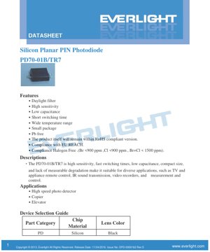
1. Product Overview
The PD70-01B/TR7 is a high-performance Silicon Planar PIN Photodiode designed for applications requiring fast response and high sensitivity to infrared light. Its compact size and robust performance across a wide temperature range make it a versatile component for various electronic systems.
1.1 Core Advantages and Target Market
This photodiode offers several key advantages, including a built-in daylight filter to reduce ambient light interference, high sensitivity at its peak wavelength, and very low junction capacitance enabling short switching times. Its small, surface-mount package is Pb-free and compliant with RoHS, REACH, and halogen-free standards. These features make it particularly suitable for consumer electronics, industrial control, and communication applications such as television and appliance remote controls, infrared audio transmission, video recorders, copiers, elevator sensors, and general-purpose measurement and control systems.
2. Technical Parameter Deep Dive
2.1 Absolute Maximum Ratings
The device is designed to operate reliably within specified limits. The maximum reverse voltage (VR) is 32V. It can function in an operating temperature (Topr) range of -25°C to +85°C and be stored (Tstg) from -40°C to +85°C. The maximum soldering temperature (Tsol) is 260°C for a duration not exceeding 5 seconds. The power dissipation (Pd) is rated at 150 mW at or below 25°C free air temperature.
2.2 Electro-Optical Characteristics
At a standard temperature of 25°C, the photodiode exhibits specific performance metrics. Its spectral bandwidth (λ0.5) ranges from 730 nm to 1100 nm, with peak sensitivity (λP) at 940 nm, placing it firmly in the near-infrared spectrum. Under an irradiance of 1 mW/cm² at 940 nm, the typical short-circuit current (ISC) is 35 µA, and the typical reverse light current (IL) at VR=5V is 25 µA (min. 17 µA). The reverse dark current (ID) at VR=10V is typically 5 nA, with a maximum of 30 nA. The reverse breakdown voltage (VBR) is minimum 32V, typically 170V at a current of 100 µA.
3. Performance Curve Analysis
The datasheet includes typical characteristic curves that provide deeper insight into device behavior beyond the tabulated minimum, typical, and maximum values.
3.1 Spectral Sensitivity
A graph (Fig.1) illustrates the normalized spectral response versus wavelength. The curve shows a sharp rise in sensitivity starting around 730 nm, peaking at 940 nm, and then gradually falling off towards 1100 nm. This confirms its optimization for infrared detection, particularly for common 940 nm IR emitters, while the daylight filter attenuates sensitivity in the visible spectrum.
3.2 Linearity of Response
Another graph (Fig.2) plots the Reverse Light Current (IL) against Irradiance (Ee). This curve is expected to show a highly linear relationship, indicating that the photocurrent output is directly proportional to the incident light power over the operational range, a critical feature for measurement and control applications.
4. Mechanical and Package Information
4.1 Package Dimensions and Polarity
The PD70-01B/TR7 comes in a compact surface-mount package. Detailed dimensional drawings are provided. The package body dimensions are approximately 2.0 mm in length, 1.25 mm in width, and 0.9 mm in height (excluding leads). The cathode is typically marked, often by a notch, a beveled edge, or a dot on the package. Designers must consult the detailed package drawing for the exact polarity identification marker and pad layout to ensure correct PCB footprint design and assembly orientation.
4.2 Carrier Tape and Reel Specifications
For automated assembly, the component is supplied in carrier tape and reel. The tape width, pocket dimensions, and reel diameter are specified to be compatible with standard pick-and-place equipment. The standard packing quantity is 1000 pieces per reel.
5. Soldering and Assembly Guidelines
5.1 Reflow Soldering Profile
For Pb-free soldering, a specific temperature profile must be followed. The recommended profile includes a preheat stage, a soak zone, a peak reflow temperature not exceeding 260°C, and a controlled cooling phase. The total time above liquidus and the maximum peak temperature duration are critical to prevent thermal damage to the epoxy package and the semiconductor die. Reflow soldering should not be performed more than two times.
5.2 Hand Soldering and Rework
If hand soldering is necessary, extreme care must be taken. The soldering iron tip temperature should be below 350°C, and contact time with each terminal should be less than 3 seconds per solder joint using an iron with a capacity of 25W or less. A cooling interval of more than two seconds is required between soldering each terminal. For rework, a double-head soldering iron is recommended to simultaneously heat both terminals and avoid mechanical stress. The feasibility and impact of rework on device characteristics should be evaluated beforehand.
6. Storage and Handling Precautions
6.1 Moisture Sensitivity
This device is moisture-sensitive. The moisture barrier bag should not be opened until the components are ready for use. Before opening, storage conditions should be 30°C or less and 90% Relative Humidity (RH) or less. The total shelf life in the unopened bag is one year. After opening, the components must be stored at 30°C or less and 60% RH or less and used within 168 hours (7 days). If the silica gel desiccant indicates saturation or the storage time is exceeded, a baking treatment at 60 ±5°C for 24 hours is required before use.
6.2 Electrical Protection
A critical precaution is over-current protection. As a diode, it must be operated with a series current-limiting resistor when biased. Without this resistor, a small increase in applied voltage can cause a large, potentially destructive increase in current, leading to burnout. The resistor value must be calculated based on the operating voltage and the desired photocurrent or dark current.
7. Application Suggestions and Design Considerations
7.1 Typical Application Circuits
The PD70-01B/TR7 can be used in two primary configurations: photovoltaic mode (zero bias) and photoconductive mode (reverse bias). In photovoltaic mode, it generates a voltage/current when illuminated, suitable for simple light detection. In photoconductive mode (with a reverse bias voltage applied, e.g., 5V), the response speed is significantly faster, and the linearity is improved, making it ideal for high-speed pulse detection like in IR remote controls. A transimpedance amplifier (TIA) circuit is commonly used to convert the small photocurrent into a usable voltage signal.
7.2 Design Considerations
Key design factors include: Biasing: Choose the operating mode based on speed and linearity requirements. Bandwidth: The low capacitance (implied by fast switching time) allows for high bandwidth when paired with a suitable low-noise amplifier. Optical Filtering: The built-in daylight filter is beneficial, but for specific applications, additional external optical filters may be needed to block unwanted wavelengths. PCB Layout: Keep the photodiode and its amplifier close together to minimize parasitic capacitance and noise pickup. Ensure the anode and cathode are correctly oriented according to the package marking.
8. Technical Comparison and Differentiation
Compared to standard photodiodes or phototransistors, the PIN structure of the PD70-01B/TR7 offers distinct advantages. The intrinsic (I) region between the P and N layers reduces junction capacitance, enabling faster response times (short switching time). This makes it superior for high-speed data transmission via IR. Its high sensitivity and specified dark current parameters provide a good signal-to-noise ratio. The integrated daylight filter is a practical feature not found in all basic photodiodes, simplifying design for ambient light environments.
9. Frequently Asked Questions (FAQ)
9.1 What is the purpose of the daylight filter?
The daylight filter attenuates sensitivity in the visible light spectrum (approximately 400-700 nm). This reduces noise and interference from ambient light sources like sunlight or room lighting, allowing the device to more reliably detect the modulated infrared signals from a remote control or other IR source.
9.2 How do I choose the value of the series resistor?
The series resistor limits the current under both dark and illuminated conditions. In reverse bias mode, the resistor value (R) can be estimated using Ohm's Law: R ≈ (Supply Voltage - Diode Reverse Voltage Drop) / Maximum Expected Current. The current should be kept well below the maximum power dissipation limit. Start with a conservative value (e.g., 10kΩ) and adjust based on signal amplitude and speed requirements.
9.3 Can this sensor detect visible light?
While its spectral range starts at 730 nm (border of red visible light), its sensitivity in the visible spectrum is very low due to the daylight filter. It is primarily an infrared detector optimized for 940 nm. For visible light detection, a photodiode without an IR-blocking or daylight filter would be required.
10. Operating Principle Introduction
A Silicon PIN Photodiode is a semiconductor device that converts light into electrical current. When photons with energy greater than the bandgap of silicon strike the device, they generate electron-hole pairs in the depletion region. In a PIN structure, a wide intrinsic (I) region is sandwiched between the P-type and N-type regions. This wide I-region creates a larger depletion area for photon absorption and, crucially, reduces the junction capacitance. Under reverse bias, the electric field sweeps these charge carriers to the contacts, generating a photocurrent that is proportional to the incident light intensity. The "planar" process refers to the manufacturing technique, which typically yields devices with stable and consistent performance.
LED Specification Terminology
Complete explanation of LED technical terms
Photoelectric Performance
| Term | Unit/Representation | Simple Explanation | Why Important |
|---|---|---|---|
| Luminous Efficacy | lm/W (lumens per watt) | Light output per watt of electricity, higher means more energy efficient. | Directly determines energy efficiency grade and electricity cost. |
| Luminous Flux | lm (lumens) | Total light emitted by source, commonly called "brightness". | Determines if the light is bright enough. |
| Viewing Angle | ° (degrees), e.g., 120° | Angle where light intensity drops to half, determines beam width. | Affects illumination range and uniformity. |
| CCT (Color Temperature) | K (Kelvin), e.g., 2700K/6500K | Warmth/coolness of light, lower values yellowish/warm, higher whitish/cool. | Determines lighting atmosphere and suitable scenarios. |
| CRI / Ra | Unitless, 0–100 | Ability to render object colors accurately, Ra≥80 is good. | Affects color authenticity, used in high-demand places like malls, museums. |
| SDCM | MacAdam ellipse steps, e.g., "5-step" | Color consistency metric, smaller steps mean more consistent color. | Ensures uniform color across same batch of LEDs. |
| Dominant Wavelength | nm (nanometers), e.g., 620nm (red) | Wavelength corresponding to color of colored LEDs. | Determines hue of red, yellow, green monochrome LEDs. |
| Spectral Distribution | Wavelength vs intensity curve | Shows intensity distribution across wavelengths. | Affects color rendering and quality. |
Electrical Parameters
| Term | Symbol | Simple Explanation | Design Considerations |
|---|---|---|---|
| Forward Voltage | Vf | Minimum voltage to turn on LED, like "starting threshold". | Driver voltage must be ≥Vf, voltages add up for series LEDs. |
| Forward Current | If | Current value for normal LED operation. | Usually constant current drive, current determines brightness & lifespan. |
| Max Pulse Current | Ifp | Peak current tolerable for short periods, used for dimming or flashing. | Pulse width & duty cycle must be strictly controlled to avoid damage. |
| Reverse Voltage | Vr | Max reverse voltage LED can withstand, beyond may cause breakdown. | Circuit must prevent reverse connection or voltage spikes. |
| Thermal Resistance | Rth (°C/W) | Resistance to heat transfer from chip to solder, lower is better. | High thermal resistance requires stronger heat dissipation. |
| ESD Immunity | V (HBM), e.g., 1000V | Ability to withstand electrostatic discharge, higher means less vulnerable. | Anti-static measures needed in production, especially for sensitive LEDs. |
Thermal Management & Reliability
| Term | Key Metric | Simple Explanation | Impact |
|---|---|---|---|
| Junction Temperature | Tj (°C) | Actual operating temperature inside LED chip. | Every 10°C reduction may double lifespan; too high causes light decay, color shift. |
| Lumen Depreciation | L70 / L80 (hours) | Time for brightness to drop to 70% or 80% of initial. | Directly defines LED "service life". |
| Lumen Maintenance | % (e.g., 70%) | Percentage of brightness retained after time. | Indicates brightness retention over long-term use. |
| Color Shift | Δu′v′ or MacAdam ellipse | Degree of color change during use. | Affects color consistency in lighting scenes. |
| Thermal Aging | Material degradation | Deterioration due to long-term high temperature. | May cause brightness drop, color change, or open-circuit failure. |
Packaging & Materials
| Term | Common Types | Simple Explanation | Features & Applications |
|---|---|---|---|
| Package Type | EMC, PPA, Ceramic | Housing material protecting chip, providing optical/thermal interface. | EMC: good heat resistance, low cost; Ceramic: better heat dissipation, longer life. |
| Chip Structure | Front, Flip Chip | Chip electrode arrangement. | Flip chip: better heat dissipation, higher efficacy, for high-power. |
| Phosphor Coating | YAG, Silicate, Nitride | Covers blue chip, converts some to yellow/red, mixes to white. | Different phosphors affect efficacy, CCT, and CRI. |
| Lens/Optics | Flat, Microlens, TIR | Optical structure on surface controlling light distribution. | Determines viewing angle and light distribution curve. |
Quality Control & Binning
| Term | Binning Content | Simple Explanation | Purpose |
|---|---|---|---|
| Luminous Flux Bin | Code e.g., 2G, 2H | Grouped by brightness, each group has min/max lumen values. | Ensures uniform brightness in same batch. |
| Voltage Bin | Code e.g., 6W, 6X | Grouped by forward voltage range. | Facilitates driver matching, improves system efficiency. |
| Color Bin | 5-step MacAdam ellipse | Grouped by color coordinates, ensuring tight range. | Guarantees color consistency, avoids uneven color within fixture. |
| CCT Bin | 2700K, 3000K etc. | Grouped by CCT, each has corresponding coordinate range. | Meets different scene CCT requirements. |
Testing & Certification
| Term | Standard/Test | Simple Explanation | Significance |
|---|---|---|---|
| LM-80 | Lumen maintenance test | Long-term lighting at constant temperature, recording brightness decay. | Used to estimate LED life (with TM-21). |
| TM-21 | Life estimation standard | Estimates life under actual conditions based on LM-80 data. | Provides scientific life prediction. |
| IESNA | Illuminating Engineering Society | Covers optical, electrical, thermal test methods. | Industry-recognized test basis. |
| RoHS / REACH | Environmental certification | Ensures no harmful substances (lead, mercury). | Market access requirement internationally. |
| ENERGY STAR / DLC | Energy efficiency certification | Energy efficiency and performance certification for lighting. | Used in government procurement, subsidy programs, enhances competitiveness. |