Table of Contents
- 1. Product Overview
- 1.1 Core Advantages and Product Positioning
- 1.2 Compliance and Environmental Specifications
- 1.3 Manufacturing and Compatibility
- 2. Technical Parameters: In-Depth Objective Interpretation
- 2.1 Absolute Maximum Ratings
- 2.2 Electro-Optical Characteristics
- 3. Binning System Explanation
- 3.1 Luminous Intensity Binning
- 3.2 Dominant Wavelength Binning
- 3.3 Forward Voltage Binning
- 4. Performance Curve Analysis
- 4.1 Current vs. Voltage (I-V) Curve
- 4.2 Luminous Intensity vs. Forward Current (Iv-IF)
- 4.3 Spectral Distribution
- 4.4 Temperature Dependence
- 5. Mechanical and Package Information
- 5.1 Package Dimensions
- 5.2 Polarity Identification
- 6. Soldering and Assembly Guidelines
- 6.1 Reflow Soldering Profile
- 6.2 Hand Soldering Precautions
- 6.3 Storage and Moisture Sensitivity
- 6.4 Design and Assembly Stress
- 7. Packaging and Ordering Information
- 7.1 Tape and Reel Specifications
- 7.2 Label Explanation
- 8. Application Suggestions
- 8.1 Typical Application Scenarios
- 8.2 Design Considerations and Notes
- 8.3 Application Restrictions
- 9. Technical Comparison and Differentiation
- 9.1 Key Differentiating Advantages
- 9.2 Considerations vs. Larger Packages
- 10. Frequently Asked Questions (Based on Technical Parameters)
- 11. Practical Design and Usage Case
- 11.1 Case Study: Low-Power Status Indicator Panel
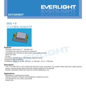
1. Product Overview
The 17-21 series is a compact, surface-mount device (SMD) light-emitting diode (LED) utilizing an InGaN (Indium Gallium Nitride) chip to produce blue light. This component is designed for modern, automated electronics manufacturing, offering significant advantages in board space utilization and assembly efficiency compared to traditional leaded packages.
1.1 Core Advantages and Product Positioning
The primary advantage of the 17-21 SMD LED is its miniature footprint. The significantly smaller size compared to lead-frame type LEDs enables several key benefits for product designers and manufacturers. It allows for smaller printed circuit board (PCB) designs, which is critical for modern compact electronic devices. Furthermore, it supports higher packing density, meaning more components can be placed on a single board, optimizing functionality within a limited space. This also translates to reduced requirements for storage space for both components and finished products. Ultimately, these factors contribute to the development of smaller, lighter, and more portable end-user equipment. The lightweight nature of the SMD package makes it particularly suitable for miniature and portable applications where weight is a critical factor.
1.2 Compliance and Environmental Specifications
This product is designed with modern environmental and regulatory standards in mind. It is a Pb-free (lead-free) component, aligning with global restrictions on hazardous substances. The product itself remains compliant with the RoHS (Restriction of Hazardous Substances) directive. It also complies with the EU REACH (Registration, Evaluation, Authorisation and Restriction of Chemicals) regulation. Additionally, it is classified as Halogen Free, with strict limits on bromine (Br) and chlorine (Cl) content: less than 900 ppm for each individually, and a combined total of less than 1500 ppm for Br+Cl.
1.3 Manufacturing and Compatibility
The LED is supplied packaged in 8mm tape on 7-inch diameter reels, which is the standard for high-volume, automated pick-and-place assembly lines. This packaging format ensures compatibility with automatic placement equipment, streamlining the production process. The component is also compatible with standard infrared and vapor phase reflow soldering processes, which are the predominant methods for attaching SMD components to PCBs. It is a mono-color type, emitting light in the blue spectrum.
2. Technical Parameters: In-Depth Objective Interpretation
This section provides a detailed, objective analysis of the electrical, optical, and thermal parameters defined in the datasheet, explaining their significance for circuit design and reliability.
2.1 Absolute Maximum Ratings
The Absolute Maximum Ratings define the stress limits beyond which permanent damage to the device may occur. These are not conditions for normal operation but rather thresholds that must never be exceeded.
- Reverse Voltage (VR): 5V - Applying a reverse bias voltage greater than 5V can cause junction breakdown. The datasheet explicitly notes that the device is not designed for reverse operation; the VR rating is only applied during the reverse current (IR) test condition.
- Forward Current (IF): 10mA - This is the maximum continuous DC forward current recommended for reliable long-term operation.
- Peak Forward Current (IFP): 40mA - This rating applies under pulsed conditions with a duty cycle of 1/10 at 1 kHz. It indicates the device can handle short, high-current pulses, which might be used for brightness flashing or multiplexing schemes.
- Power Dissipation (Pd): 40mW - This is the maximum power the package can dissipate as heat at an ambient temperature (Ta) of 25°C. Exceeding this limit risks overheating and accelerated degradation of the LED chip.
- Electrostatic Discharge (ESD): 150V (HBM) - This specifies the Human Body Model ESD withstand voltage. It indicates a moderate level of ESD sensitivity; proper handling procedures (e.g., grounded workstations, wrist straps) are necessary to prevent damage from static electricity.
- Operating Temperature (Topr): -40°C to +85°C - The LED is rated to function correctly within this wide ambient temperature range, suitable for consumer, industrial, and some automotive applications (excluding safety-critical systems).
- Storage Temperature (Tstg): -40°C to +90°C - The device can be stored without degradation within this temperature range when not powered.
- Soldering Temperature (Tsol):
- Reflow Soldering: Peak temperature of 260°C for a maximum of 10 seconds.
- Hand Soldering: Iron tip temperature up to 350°C for a maximum of 3 seconds per terminal.
2.2 Electro-Optical Characteristics
These parameters are measured at a standard test condition of Ta=25°C and IF=5mA, unless otherwise specified. They define the core light output and electrical performance.
- Luminous Intensity (Iv): 11.5 mcd (Min) to 28.5 mcd (Max) - This is the perceived brightness of the LED as measured in millicandelas. The wide range indicates a significant variation between individual units, which is managed through the binning system described later. The typical value is not specified in the table.
- Viewing Angle (2θ1/2): 140° (Typical) - This very wide viewing angle indicates the LED emits light over a broad hemisphere. The intensity is measured at the angle where it drops to half of its peak value (hence 2θ1/2).
- Peak Wavelength (λp): 468 nm (Typical) - The wavelength at which the spectral power distribution of the emitted light is at its maximum. This is a physical property of the InGaN semiconductor material.
- Dominant Wavelength (λd): 465.0 nm to 470.0 nm - This is the single wavelength that the human eye perceives as matching the color of the LED's light. It is the key parameter for color specification. The tolerance is ±1nm.
- Spectral Radiation Bandwidth (Δλ): 25 nm (Typical) - This measures the width of the emitted spectrum at half its maximum power (Full Width at Half Maximum - FWHM). A value of 25nm is characteristic of a blue InGaN LED, indicating a relatively pure spectral color.
- Forward Voltage (VF): 2.7V (Min) to 3.1V (Max) - The voltage drop across the LED when conducting the specified forward current (5mA). This parameter is crucial for designing the current-limiting circuit (usually a resistor). The tolerance is ±0.1V.
- Reverse Current (IR): 50 μA (Max) - The small leakage current that flows when the maximum reverse voltage (5V) is applied. This test is for characterization only.
3. Binning System Explanation
To manage the natural variations in the manufacturing process, LEDs are sorted into performance bins. This allows designers to select components with consistent characteristics for their application.
3.1 Luminous Intensity Binning
LEDs are sorted based on their measured luminous intensity at IF=5mA.
- Bin Code L: Minimum 11.5 mcd, Maximum 18.0 mcd.
- Bin Code M: Minimum 18.0 mcd, Maximum 28.5 mcd.
The tolerance for luminous intensity is ±11%. Designers requiring higher and more consistent brightness would specify Bin M.
3.2 Dominant Wavelength Binning
LEDs are sorted based on their dominant wavelength to ensure color consistency.
- Bin Code X: Minimum 465.0 nm, Maximum 470.0 nm.
The tolerance for dominant wavelength is ±1nm. All units fall within a tight 5nm range, ensuring a uniform blue hue.
3.3 Forward Voltage Binning
LEDs are sorted based on their forward voltage drop at IF=5mA. This is important for power supply design and ensuring uniform current distribution when multiple LEDs are connected in parallel.
- Bin Code 10: Minimum 2.7V, Maximum 2.9V.
- Bin Code 11: Minimum 2.9V, Maximum 3.1V.
The tolerance for forward voltage is ±0.1V. Selecting LEDs from the same voltage bin minimizes brightness variations in parallel arrays.
4. Performance Curve Analysis
The datasheet references "Typical Electro-Optical Characteristics Curves." While the specific graphs are not provided in the text, we can infer their standard content and significance.
4.1 Current vs. Voltage (I-V) Curve
A typical I-V curve would show the relationship between forward current (IF) and forward voltage (VF). It demonstrates the exponential nature of the diode. The curve allows designers to determine the VF for any given operating current within the rated range, which is essential for calculating the correct series current-limiting resistor value: R = (Vsupply - VF) / IF.
4.2 Luminous Intensity vs. Forward Current (Iv-IF)
This curve shows how light output increases with forward current. It is typically linear over a range but will saturate at higher currents due to thermal and efficiency effects. This graph helps designers choose an operating point that balances brightness with power consumption and device lifetime.
4.3 Spectral Distribution
A spectral distribution plot would show the relative optical power emitted as a function of wavelength. It would center around the typical peak wavelength of 468nm with a FWHM of approximately 25nm, confirming the monochromatic blue output.
4.4 Temperature Dependence
Curves showing the variation of forward voltage and luminous intensity with junction temperature are critical for understanding performance in real-world environments. Typically, VF decreases with increasing temperature (negative temperature coefficient), while luminous intensity also decreases as temperature rises.
5. Mechanical and Package Information
5.1 Package Dimensions
The 17-21 SMD LED has a very compact footprint. Key dimensions (in mm) include a body length of 1.6, width of 0.8, and height of 0.6. The package features two solderable terminals (anode and cathode) on the bottom. A cathode mark is indicated on the top of the package body to allow for correct polarity orientation during assembly and inspection. All unspecified tolerances are ±0.1mm.
5.2 Polarity Identification
Correct polarity is essential for LED operation. The package includes a visual marker to identify the cathode (negative terminal). This is typically a green dot, a notch, or a beveled corner on the top of the LED body. The PCB footprint design must align with this marking to ensure proper electrical connection.
6. Soldering and Assembly Guidelines
Proper handling and soldering are critical to maintaining the reliability and performance of SMD LEDs.
6.1 Reflow Soldering Profile
The recommended Pb-free reflow profile is provided:
- Pre-heating: Ramp from ambient to 150-200°C over 60-120 seconds.
- Soak/Reflow: Time above 217°C (liquidus temperature for Pb-free solder) should be 60-150 seconds. The peak temperature must not exceed 260°C, and the time at or above 255°C must not exceed 30 seconds.
- Cooling: The maximum cooling rate should be 6°C per second.
- Important: Reflow soldering should not be performed more than two times on the same device.
6.2 Hand Soldering Precautions
If hand soldering is necessary, extreme care must be taken:
- Use a soldering iron with a tip temperature less than 350°C.
- Apply heat to each terminal for a maximum of 3 seconds.
- Use an iron with a capacity of 25W or less.
- Allow an interval of at least 2 seconds between soldering each terminal to prevent heat buildup.
- The datasheet cautions that damage often occurs during hand soldering.
6.3 Storage and Moisture Sensitivity
The LEDs are packaged in moisture-resistant barrier bags with desiccant to prevent absorption of atmospheric moisture, which can cause "popcorning" (package cracking) during reflow.
- Do not open the moisture-proof bag until the products are ready for use.
- After opening: Store at ≤30°C and ≤60% Relative Humidity.
- Floor Life: Use within 168 hours (7 days) after opening. Unused LEDs must be resealed in a moisture-proof package.
- Baking: If the desiccant indicator has changed color or the floor life is exceeded, bake the LEDs at 60 ±5°C for 24 hours to remove moisture before soldering.
6.4 Design and Assembly Stress
- Current Limiting: An external current-limiting resistor is mandatory. The LED's exponential I-V characteristic means a small increase in voltage causes a large increase in current, leading to immediate burnout without a resistor.
- Mechanical Stress: Do not apply mechanical stress to the LED during heating (soldering) or by warping the circuit board after assembly.
- Repair: Repair after soldering is not recommended. If unavoidable, use a dual-head soldering iron to simultaneously heat both terminals and lift the component without stressing one side. Verify device characteristics after any repair attempt.
7. Packaging and Ordering Information
7.1 Tape and Reel Specifications
The LEDs are supplied in embossed carrier tape for automated handling.
- Carrier Tape Width: 8mm.
- Reel Diameter: 7 inches.
- Quantity per Reel: 3000 pieces.
- Detailed dimensions for the carrier tape pockets and the reel are provided in the datasheet drawings.
7.2 Label Explanation
The reel and bag labels contain critical information for traceability and correct application:
- CPN: Customer's Product Number (as assigned by the buyer).
- P/N: Manufacturer's Product Number.
- QTY: Packing Quantity (e.g., 3000).
- CAT: Luminous Intensity Rank (e.g., L or M).
- HUE: Chromaticity Coordinates & Dominant Wavelength Rank (e.g., X).
- REF: Forward Voltage Rank (e.g., 10 or 11).
- LOT No: Manufacturing Lot Number for traceability.
8. Application Suggestions
8.1 Typical Application Scenarios
The datasheet lists several key applications suited to the 17-21 blue LED's characteristics:
- Backlighting: For instrument panel dashboards, membrane switches, and control panels where a small, bright indicator is needed.
- Telecommunication Equipment: As status indicators or backlights for buttons on telephones, fax machines, and networking gear.
- Flat Backlighting: For small LCD displays, switch legends, and symbols, often in conjunction with a light guide.
- General Indicator Use: Any application requiring a compact, reliable, blue status or indicator light.
8.2 Design Considerations and Notes
- Current Drive Circuit: Always use a series resistor. Calculate based on the maximum VF from the bin (e.g., 3.1V) to ensure sufficient current limiting under worst-case conditions.
- Thermal Management:
- Viewing Angle: The 140° viewing angle provides very wide visibility, which is excellent for panel indicators but may require light guides or diffusers if a more focused beam is desired.
- ESD Protection: Implement ESD protection on input lines if the LED is connected to user-accessible ports, or ensure strict ESD controls during handling and assembly.
8.3 Application Restrictions
The datasheet includes a critical disclaimer regarding high-reliability applications. This product may not be suitable for use in:
- Military/Aerospace systems.
- Automotive Safety/Security systems (e.g., airbag controls, brake lights).
- Medical Life-Support or Critical-Care equipment.
For these applications, components with different qualifications, tighter tolerances, and higher reliability ratings are required. Designers must contact the manufacturer to discuss suitability for any application beyond standard consumer/industrial use.
9. Technical Comparison and Differentiation
While a direct comparison with other products is not in the datasheet, we can objectively highlight the key differentiators of the 17-21 series based on its specifications.
9.1 Key Differentiating Advantages
- Extreme Miniaturization: The 1.6x0.8mm footprint is among the smallest SMD LED packages, enabling ultra-compact designs.
- Wide Viewing Angle: The 140° viewing angle is exceptionally broad, providing excellent off-axis visibility compared to many LEDs with narrower beams.
- Halogen-Free Compliance: Meets stringent halogen-free requirements, which is increasingly important for environmentally conscious designs and certain market regulations.
- Comprehensive Binning: Offers binning for intensity, wavelength, and voltage, allowing for high consistency in mass production applications.
9.2 Considerations vs. Larger Packages
Compared to larger SMD LEDs (e.g., 3528, 5050):
- Lower Maximum Power: The 40mW Pd rating is lower than larger packages, limiting maximum brightness.
- Thermal Performance: The smaller size may have higher thermal resistance, making heat dissipation more critical at higher drive currents.
- Handling Difficulty: The tiny size makes manual prototyping and rework more challenging.
10. Frequently Asked Questions (Based on Technical Parameters)
Q1: What resistor value should I use with a 5V supply? A: Using the maximum VF of 3.1V (Bin 11) and a target current of 5mA: R = (5V - 3.1V) / 0.005A = 380 Ohms. The nearest standard value is 390 Ohms. Recalculate with the minimum VF (2.7V) to check current: I = (5-2.7)/390 ≈ 5.9mA, which is safe. A 390Ω resistor is a good starting point.
Q2: Can I drive this LED at 20mA for higher brightness? A: No. The Absolute Maximum Rating for continuous forward current (IF) is 10mA. Operating at 20mA would exceed this rating, significantly reducing lifetime and likely causing immediate failure. For higher brightness, select an LED rated for higher current or use pulsed operation within the IFP rating (40mA at 1/10 duty cycle).
Q3: The LED works after hand soldering but is dim. Why? A: This is a classic sign of thermal damage from excessive soldering heat or time. The high temperature can degrade the semiconductor chip or the wire bonds inside the package. Always adhere strictly to the hand soldering guidelines (350°C max, 3 seconds max per terminal).
Q4: My batch of LEDs has slightly different blue colors. Is this normal? A: Yes, there is inherent variation. This is why the Dominant Wavelength bin (HUE=X, 465-470nm) exists. For applications requiring perfect color matching (e.g., multi-LED displays), you must specify and use LEDs from the same manufacturing lot and ensure your supplier provides tight binning.
11. Practical Design and Usage Case
11.1 Case Study: Low-Power Status Indicator Panel
Scenario: Designing a compact control panel with 12 blue status indicators. Space is extremely limited, and uniform brightness/color is important for user experience. Design Decisions: 1. Component Selection: Choose the 17-21 LED for its minimal footprint. 2. Binning Specification: Order all LEDs from Bin M (higher intensity) and Bin X for wavelength. Specify all from the same voltage bin (e.g., 10) to ensure consistent current draw in parallel. 3. Circuit Design: Use a 5V rail. With VF~2.8V (Bin 10 typ), choose a 430Ω resistor for ~5mA: (5-2.8)/0.005=440Ω, 430Ω is standard. This gives ~11-18 mcd per LED. 4. PCB Layout: Place LEDs with consistent orientation relative to the cathode mark. Ensure solder pad design matches the datasheet's recommended footprint to avoid tombstoning during reflow. 5. Assembly: Use the provided reflow profile. Keep the bag sealed until the production line is ready. Use all LEDs within 7 days of opening the reel. Outcome: A dense, professional-looking panel with uniform, bright blue indicators, achieved reliably through adherence to the datasheet parameters.
LED Specification Terminology
Complete explanation of LED technical terms
Photoelectric Performance
| Term | Unit/Representation | Simple Explanation | Why Important |
|---|---|---|---|
| Luminous Efficacy | lm/W (lumens per watt) | Light output per watt of electricity, higher means more energy efficient. | Directly determines energy efficiency grade and electricity cost. |
| Luminous Flux | lm (lumens) | Total light emitted by source, commonly called "brightness". | Determines if the light is bright enough. |
| Viewing Angle | ° (degrees), e.g., 120° | Angle where light intensity drops to half, determines beam width. | Affects illumination range and uniformity. |
| CCT (Color Temperature) | K (Kelvin), e.g., 2700K/6500K | Warmth/coolness of light, lower values yellowish/warm, higher whitish/cool. | Determines lighting atmosphere and suitable scenarios. |
| CRI / Ra | Unitless, 0–100 | Ability to render object colors accurately, Ra≥80 is good. | Affects color authenticity, used in high-demand places like malls, museums. |
| SDCM | MacAdam ellipse steps, e.g., "5-step" | Color consistency metric, smaller steps mean more consistent color. | Ensures uniform color across same batch of LEDs. |
| Dominant Wavelength | nm (nanometers), e.g., 620nm (red) | Wavelength corresponding to color of colored LEDs. | Determines hue of red, yellow, green monochrome LEDs. |
| Spectral Distribution | Wavelength vs intensity curve | Shows intensity distribution across wavelengths. | Affects color rendering and quality. |
Electrical Parameters
| Term | Symbol | Simple Explanation | Design Considerations |
|---|---|---|---|
| Forward Voltage | Vf | Minimum voltage to turn on LED, like "starting threshold". | Driver voltage must be ≥Vf, voltages add up for series LEDs. |
| Forward Current | If | Current value for normal LED operation. | Usually constant current drive, current determines brightness & lifespan. |
| Max Pulse Current | Ifp | Peak current tolerable for short periods, used for dimming or flashing. | Pulse width & duty cycle must be strictly controlled to avoid damage. |
| Reverse Voltage | Vr | Max reverse voltage LED can withstand, beyond may cause breakdown. | Circuit must prevent reverse connection or voltage spikes. |
| Thermal Resistance | Rth (°C/W) | Resistance to heat transfer from chip to solder, lower is better. | High thermal resistance requires stronger heat dissipation. |
| ESD Immunity | V (HBM), e.g., 1000V | Ability to withstand electrostatic discharge, higher means less vulnerable. | Anti-static measures needed in production, especially for sensitive LEDs. |
Thermal Management & Reliability
| Term | Key Metric | Simple Explanation | Impact |
|---|---|---|---|
| Junction Temperature | Tj (°C) | Actual operating temperature inside LED chip. | Every 10°C reduction may double lifespan; too high causes light decay, color shift. |
| Lumen Depreciation | L70 / L80 (hours) | Time for brightness to drop to 70% or 80% of initial. | Directly defines LED "service life". |
| Lumen Maintenance | % (e.g., 70%) | Percentage of brightness retained after time. | Indicates brightness retention over long-term use. |
| Color Shift | Δu′v′ or MacAdam ellipse | Degree of color change during use. | Affects color consistency in lighting scenes. |
| Thermal Aging | Material degradation | Deterioration due to long-term high temperature. | May cause brightness drop, color change, or open-circuit failure. |
Packaging & Materials
| Term | Common Types | Simple Explanation | Features & Applications |
|---|---|---|---|
| Package Type | EMC, PPA, Ceramic | Housing material protecting chip, providing optical/thermal interface. | EMC: good heat resistance, low cost; Ceramic: better heat dissipation, longer life. |
| Chip Structure | Front, Flip Chip | Chip electrode arrangement. | Flip chip: better heat dissipation, higher efficacy, for high-power. |
| Phosphor Coating | YAG, Silicate, Nitride | Covers blue chip, converts some to yellow/red, mixes to white. | Different phosphors affect efficacy, CCT, and CRI. |
| Lens/Optics | Flat, Microlens, TIR | Optical structure on surface controlling light distribution. | Determines viewing angle and light distribution curve. |
Quality Control & Binning
| Term | Binning Content | Simple Explanation | Purpose |
|---|---|---|---|
| Luminous Flux Bin | Code e.g., 2G, 2H | Grouped by brightness, each group has min/max lumen values. | Ensures uniform brightness in same batch. |
| Voltage Bin | Code e.g., 6W, 6X | Grouped by forward voltage range. | Facilitates driver matching, improves system efficiency. |
| Color Bin | 5-step MacAdam ellipse | Grouped by color coordinates, ensuring tight range. | Guarantees color consistency, avoids uneven color within fixture. |
| CCT Bin | 2700K, 3000K etc. | Grouped by CCT, each has corresponding coordinate range. | Meets different scene CCT requirements. |
Testing & Certification
| Term | Standard/Test | Simple Explanation | Significance |
|---|---|---|---|
| LM-80 | Lumen maintenance test | Long-term lighting at constant temperature, recording brightness decay. | Used to estimate LED life (with TM-21). |
| TM-21 | Life estimation standard | Estimates life under actual conditions based on LM-80 data. | Provides scientific life prediction. |
| IESNA | Illuminating Engineering Society | Covers optical, electrical, thermal test methods. | Industry-recognized test basis. |
| RoHS / REACH | Environmental certification | Ensures no harmful substances (lead, mercury). | Market access requirement internationally. |
| ENERGY STAR / DLC | Energy efficiency certification | Energy efficiency and performance certification for lighting. | Used in government procurement, subsidy programs, enhances competitiveness. |