Table of Contents
- 1. Product Overview
- 2. Technical Parameter Deep Dive
- 2.1 Absolute Maximum Ratings
- 2.2 Electro-Optical Characteristics
- 3. Binning System Explanation
- 3.1 Luminous Intensity Binning
- 3.2 Dominant Wavelength Binning
- 4. Performance Curve Analysis
- 5. Mechanical and Packaging Information
- 5.1 Package Dimension
- 5.2 Reel and Tape Dimensions
- 5.3 Label Explanation
- 6. Soldering and Assembly Guidelines
- 6.1 Storage and Handling
- 6.2 Reflow Soldering Profile
- 6.3 Hand Soldering and Repair
- 7. Application Suggestions
- 7.1 Typical Application Scenarios
- 7.2 Design Considerations
- 7.3 Application Restrictions
- 8. Frequently Asked Questions (Based on Technical Parameters)
- 9. Working Principle Introduction
- 10. Technology Trends
1. Product Overview
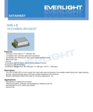
The 19-213/BHC-AP1Q2/3T is a surface-mount device (SMD) LED designed for modern electronic applications requiring compact, efficient, and reliable light sources. This component is a mono-color type, specifically emitting blue light, and is constructed using Pb-free materials, ensuring compliance with contemporary environmental and safety standards such as RoHS, EU REACH, and halogen-free requirements (Br <900 ppm, Cl <900 ppm, Br+Cl < 1500 ppm).
The primary advantage of this SMD LED lies in its miniature footprint, which is significantly smaller than traditional lead-frame type LEDs. This reduction in size enables designers to achieve smaller printed circuit board (PCB) layouts, higher component packing density, reduced storage space requirements, and ultimately, the development of more compact end-user equipment. Furthermore, its lightweight construction makes it an ideal choice for applications where minimizing weight is a critical factor.
The device is supplied in industry-standard 8mm tape on 7-inch diameter reels, ensuring compatibility with high-speed automatic pick-and-place equipment commonly used in volume manufacturing. It is also designed to be compatible with standard infrared (IR) and vapor phase reflow soldering processes, facilitating easy integration into automated assembly lines.
2. Technical Parameter Deep Dive
2.1 Absolute Maximum Ratings
The absolute maximum ratings define the limits beyond which permanent damage to the device may occur. These values are specified at an ambient temperature (Ta) of 25°C and must not be exceeded under any operating conditions.
- Reverse Voltage (VR): 5 V. The LED is not designed for reverse operation; exceeding this voltage can cause immediate failure.
- Forward Current (IF): 20 mA. This is the recommended continuous operating current.
- Peak Forward Current (IFP): 40 mA. This is permissible only under pulsed conditions with a duty cycle of 1/10 at 1 kHz.
- Power Dissipation (Pd): 75 mW. This is the maximum power the package can dissipate without exceeding its thermal limits.
- Electrostatic Discharge (ESD) Human Body Model (HBM): 150 V. Proper ESD handling procedures are essential to prevent latent damage.
- Operating Temperature (Topr): -40°C to +85°C. The device is rated for operation within this wide temperature range.
- Storage Temperature (Tstg): -40°C to +90°C.
- Soldering Temperature (Tsol): For reflow soldering, a peak temperature of 260°C for a maximum of 10 seconds is specified. For hand soldering, the iron tip temperature should not exceed 350°C for a maximum of 3 seconds per terminal.
2.2 Electro-Optical Characteristics
The electro-optical characteristics are measured at Ta=25°C and an IF of 20 mA, representing the device's typical performance under standard operating conditions.
- Luminous Intensity (Iv): The typical value is not specified as a single number; instead, the device is binned. The range spans from a minimum of 45.0 mcd to a maximum of 112.0 mcd. The viewing angle (2θ1/2) is typically 120 degrees, providing a wide beam pattern.
- Peak Wavelength (λp): Typically 468 nm, indicating the wavelength at which the spectral emission is strongest.
- Dominant Wavelength (λd): Ranges from 464.5 nm to 476.5 nm. This is the single wavelength perceived by the human eye and is also subject to binning.
- Spectral Radiation Bandwidth (Δλ): Typically 25 nm, defining the width of the emitted spectrum at half the maximum intensity (FWHM).
- Forward Voltage (VF): Ranges from 2.7 V to 3.7 V at IF=20mA. This parameter has a tolerance of ±0.1V and is also binned.
- Reverse Current (IR): Maximum 50 μA when a reverse voltage (VR) of 5V is applied. This test condition is for characterization only.
Important Notes: Tolerances are specified for key parameters: Luminous Intensity (±11%), Dominant Wavelength (±1 nm), and Forward Voltage (±0.1 V). The device is explicitly not designed for reverse operation; the VR rating applies only to the IR test.
3. Binning System Explanation
To ensure consistent color and brightness in production, the LEDs are sorted into bins based on luminous intensity and dominant wavelength.
3.1 Luminous Intensity Binning
Bins are defined by a letter-number code (P1, P2, Q1, Q2), each covering a specific range of luminous intensity measured in millicandelas (mcd) at IF=20mA.
- Bin P1: 45.0 mcd (Min) to 57.0 mcd (Max)
- Bin P2: 57.0 mcd to 72.0 mcd
- Bin Q1: 72.0 mcd to 90.0 mcd
- Bin Q2: 90.0 mcd to 112.0 mcd
3.2 Dominant Wavelength Binning
Wavelength bins are defined by an alphanumeric code (A9, A10, A11, A12), each covering a specific range of dominant wavelength measured in nanometers (nm) at IF=20mA.
- Bin A9: 464.5 nm to 467.5 nm
- Bin A10: 467.5 nm to 470.5 nm
- Bin A11: 470.5 nm to 473.5 nm
- Bin A12: 473.5 nm to 476.5 nm
This binning allows designers to select components that meet precise brightness and color consistency requirements for their application.
4. Performance Curve Analysis
The datasheet provides several typical characteristic curves that illustrate the device's behavior under varying conditions. These are essential for understanding performance in real-world scenarios.
- Relative Luminous Intensity vs. Ambient Temperature: This curve shows how light output decreases as the ambient temperature rises above 25°C. It is crucial for thermal management design to maintain desired brightness levels.
- Relative Luminous Intensity vs. Forward Current: This graph illustrates the non-linear relationship between drive current and light output. Operating above the recommended 20mA may yield diminishing returns in brightness while increasing heat and stress on the device.
- Forward Current vs. Forward Voltage (IV Curve): This fundamental curve shows the exponential relationship between voltage and current in a diode. The specified VF range (2.7V-3.7V at 20mA) is read from this curve.
- Forward Current Derating Curve: This curve dictates the maximum allowable forward current as a function of ambient temperature. As temperature increases, the maximum safe current decreases to prevent overheating.
- Spectrum Distribution: A plot of relative intensity versus wavelength, centered around the typical peak wavelength of 468 nm with a bandwidth of approximately 25 nm.
- Radiation Diagram: A polar plot depicting the spatial distribution of light intensity, confirming the typical 120-degree viewing angle.
5. Mechanical and Packaging Information
5.1 Package Dimension
The datasheet includes a detailed mechanical drawing of the LED package. The drawing specifies all critical dimensions including length, width, height, pad sizes, and their positions. Unless otherwise noted, the dimensional tolerance is ±0.1 mm. This information is vital for PCB footprint design (land pattern) to ensure proper soldering and alignment.
5.2 Reel and Tape Dimensions
The product is supplied in moisture-resistant packaging. The carrier tape dimensions are specified to hold the components securely. Each reel contains 3000 pieces. Detailed drawings of the reel (7-inch diameter), carrier tape, and cover tape are provided, all with a standard tolerance of ±0.1 mm unless stated otherwise. This ensures compatibility with automated assembly equipment.
5.3 Label Explanation
The packaging labels contain critical information for traceability and correct application:
- CPN: Customer's Product Number.
- P/N: Product Number (e.g., 19-213/BHC-AP1Q2/3T).
- QTY: Packing Quantity.
- CAT: Luminous Intensity Rank (Bin code for intensity).
- HUE: Chromaticity Coordinates & Dominant Wavelength Rank (Bin code for wavelength).
- REF: Forward Voltage Rank.
- LOT No: Manufacturing Lot Number for traceability.
The moisture-proof bag includes a desiccant and a humidity indicator card to protect the components from moisture absorption during storage and transport.
6. Soldering and Assembly Guidelines
6.1 Storage and Handling
These LEDs are moisture-sensitive. The moisture-resistant bag must not be opened until the components are ready for use. After opening:
- LEDs should be kept at ≤30°C and ≤60% Relative Humidity.
- They must be used within 168 hours (7 days).
- Unused LEDs should be resealed in a moisture-proof package with fresh desiccant.
- If the storage time is exceeded or the desiccant indicates high humidity, a baking treatment at 60 ±5°C for 24 hours is required before soldering.
6.2 Reflow Soldering Profile
A Pb-free reflow soldering temperature profile is specified:
- Pre-heating: 150-200°C for 60-120 seconds.
- Time Above Liquidus (217°C): 60-150 seconds.
- Peak Temperature: Maximum 260°C.
- Time at Peak: Maximum 10 seconds.
- Heating Rate: Maximum 6°C/sec up to 255°C, then maximum 3°C/sec to peak.
Critical Precautions: Reflow soldering should not be performed more than two times. No stress should be applied to the LEDs during heating, and the PCB should not be warped after soldering.
6.3 Hand Soldering and Repair
If hand soldering is unavoidable:
- Use a soldering iron with a tip temperature <350°C.
- Limit soldering time to ≤3 seconds per terminal.
- Use an iron with power ≤25W.
- Allow a minimum 2-second interval between soldering each terminal.
Repair after soldering is strongly discouraged. If absolutely necessary, a double-head soldering iron should be used to simultaneously heat both terminals and avoid mechanical stress. The potential for damaging the LED's characteristics during repair must be evaluated beforehand.
7. Application Suggestions
7.1 Typical Application Scenarios
Based on the datasheet, this blue SMD LED is suitable for a variety of low-to-medium power indicator and backlighting applications, including:
- Backlighting: For dashboards, switches, and symbols in consumer electronics, automotive interiors (non-critical), and industrial control panels.
- Telecommunication Equipment: Status indicators and keypad backlighting in telephones and fax machines.
- LCD Backlighting: As a flat backlight source for small monochrome or segmented LCD displays.
- General Indication: Power status, mode selection, and other user interface indicators in a wide range of electronic devices.
7.2 Design Considerations
- Current Limiting: An external current-limiting resistor is mandatory. The forward voltage has a range (2.7V-3.7V), and a small change in supply voltage can cause a large, potentially destructive change in forward current due to the diode's exponential IV characteristic. The resistor value must be calculated based on the worst-case VF (minimum) to ensure the current never exceeds the absolute maximum rating of 20mA continuous.
- Thermal Management: While the package is small, power dissipation (75mW max) and the derating curve must be considered, especially in high ambient temperature environments or enclosed spaces. Adequate PCB copper area (thermal relief pads) can help dissipate heat.
- ESD Protection: The 150V HBM ESD rating is relatively low. Implement ESD protection measures on PCBs handling these LEDs, and always follow proper ESD protocols during assembly and handling.
7.3 Application Restrictions
The datasheet explicitly states that this product is not recommended for high-reliability applications such as military/aerospace systems or automotive safety/security systems (e.g., brake lights, airbag indicators). For such applications, LEDs with corresponding automotive (AEC-Q101) or military qualifications should be selected.
8. Frequently Asked Questions (Based on Technical Parameters)
Q1: Why is a current-limiting resistor absolutely necessary?
A1: LEDs are current-driven devices. Their forward voltage (VF) has production tolerances and varies with temperature. Without a series resistor, the current is determined solely by the power supply voltage and the LED's dynamic resistance, which is very low. A slight increase in supply voltage or a decrease in VF (due to temperature rise) can cause the current to spike beyond the 20mA maximum, leading to rapid overheating and failure. The resistor provides a stable, predictable, and safe current.
Q2: How do I select the correct bin for my application?
A2: The choice depends on your requirements for brightness uniformity and color consistency. If multiple LEDs are used side-by-side (e.g., in an array or bar graph), selecting LEDs from the same luminous intensity bin (CAT) and dominant wavelength bin (HUE) is critical to avoid visible differences in brightness or shade of blue. For less critical single-indicator applications, a wider bin may be acceptable and more cost-effective.
Q3: Can I drive this LED with a pulsed current higher than 20mA to make it brighter?
A3: Yes, but only within strict limits. The datasheet specifies a Peak Forward Current (IFP) of 40mA at a 1/10 duty cycle and 1kHz frequency. Pulsing can achieve higher perceived brightness. However, you must ensure the average current over time does not exceed the continuous rating, and the junction temperature does not exceed its limits. The derating curve and power dissipation rating must still be respected.
Q4: What happens if I exceed the 7-day floor life after opening the moisture-proof bag?
A4: Plastic SMD packages can absorb moisture from the air. During reflow soldering, this trapped moisture rapidly turns to steam, which can cause internal delamination, cracking of the package, or solder joint failures ("popcorning"). If the floor life is exceeded, the components must be baked (60°C for 24 hours) to drive out the moisture before they can be safely soldered.
9. Working Principle Introduction
This LED is based on a semiconductor diode structure fabricated from Indium Gallium Nitride (InGaN) materials, as indicated in the Device Selection Guide. When a forward voltage exceeding the diode's turn-on threshold (approximately 2.7-3.7V) is applied, electrons and holes are injected into the active region of the semiconductor. These charge carriers recombine, releasing energy in the form of photons (light). The specific composition of the InGaN alloy determines the bandgap energy of the semiconductor, which directly dictates the wavelength (color) of the emitted light. In this case, the alloy is engineered to produce photons in the blue region of the visible spectrum, with a peak wavelength around 468 nm. The water-clear resin encapsulant protects the semiconductor chip and acts as a lens, shaping the emitted light into a wide 120-degree viewing angle.
10. Technology Trends
The 19-213/BHC-AP1Q2/3T represents a mature SMD LED technology. General trends in the LED industry that contextualize this component include the ongoing drive for increased efficiency (more lumens per watt), which allows for either brighter output at the same current or the same brightness with lower power consumption and less heat. There is also a trend toward higher color consistency and tighter binning to meet the demands of display and lighting applications. Furthermore, miniaturization continues, with even smaller package footprints (e.g., 0402, 0201 metric) becoming common for space-constrained applications. Finally, enhanced reliability and robustness, including higher ESD ratings and improved moisture resistance, are key development areas to expand LED use into more demanding environments like automotive lighting.
LED Specification Terminology
Complete explanation of LED technical terms
Photoelectric Performance
| Term | Unit/Representation | Simple Explanation | Why Important |
|---|---|---|---|
| Luminous Efficacy | lm/W (lumens per watt) | Light output per watt of electricity, higher means more energy efficient. | Directly determines energy efficiency grade and electricity cost. |
| Luminous Flux | lm (lumens) | Total light emitted by source, commonly called "brightness". | Determines if the light is bright enough. |
| Viewing Angle | ° (degrees), e.g., 120° | Angle where light intensity drops to half, determines beam width. | Affects illumination range and uniformity. |
| CCT (Color Temperature) | K (Kelvin), e.g., 2700K/6500K | Warmth/coolness of light, lower values yellowish/warm, higher whitish/cool. | Determines lighting atmosphere and suitable scenarios. |
| CRI / Ra | Unitless, 0–100 | Ability to render object colors accurately, Ra≥80 is good. | Affects color authenticity, used in high-demand places like malls, museums. |
| SDCM | MacAdam ellipse steps, e.g., "5-step" | Color consistency metric, smaller steps mean more consistent color. | Ensures uniform color across same batch of LEDs. |
| Dominant Wavelength | nm (nanometers), e.g., 620nm (red) | Wavelength corresponding to color of colored LEDs. | Determines hue of red, yellow, green monochrome LEDs. |
| Spectral Distribution | Wavelength vs intensity curve | Shows intensity distribution across wavelengths. | Affects color rendering and quality. |
Electrical Parameters
| Term | Symbol | Simple Explanation | Design Considerations |
|---|---|---|---|
| Forward Voltage | Vf | Minimum voltage to turn on LED, like "starting threshold". | Driver voltage must be ≥Vf, voltages add up for series LEDs. |
| Forward Current | If | Current value for normal LED operation. | Usually constant current drive, current determines brightness & lifespan. |
| Max Pulse Current | Ifp | Peak current tolerable for short periods, used for dimming or flashing. | Pulse width & duty cycle must be strictly controlled to avoid damage. |
| Reverse Voltage | Vr | Max reverse voltage LED can withstand, beyond may cause breakdown. | Circuit must prevent reverse connection or voltage spikes. |
| Thermal Resistance | Rth (°C/W) | Resistance to heat transfer from chip to solder, lower is better. | High thermal resistance requires stronger heat dissipation. |
| ESD Immunity | V (HBM), e.g., 1000V | Ability to withstand electrostatic discharge, higher means less vulnerable. | Anti-static measures needed in production, especially for sensitive LEDs. |
Thermal Management & Reliability
| Term | Key Metric | Simple Explanation | Impact |
|---|---|---|---|
| Junction Temperature | Tj (°C) | Actual operating temperature inside LED chip. | Every 10°C reduction may double lifespan; too high causes light decay, color shift. |
| Lumen Depreciation | L70 / L80 (hours) | Time for brightness to drop to 70% or 80% of initial. | Directly defines LED "service life". |
| Lumen Maintenance | % (e.g., 70%) | Percentage of brightness retained after time. | Indicates brightness retention over long-term use. |
| Color Shift | Δu′v′ or MacAdam ellipse | Degree of color change during use. | Affects color consistency in lighting scenes. |
| Thermal Aging | Material degradation | Deterioration due to long-term high temperature. | May cause brightness drop, color change, or open-circuit failure. |
Packaging & Materials
| Term | Common Types | Simple Explanation | Features & Applications |
|---|---|---|---|
| Package Type | EMC, PPA, Ceramic | Housing material protecting chip, providing optical/thermal interface. | EMC: good heat resistance, low cost; Ceramic: better heat dissipation, longer life. |
| Chip Structure | Front, Flip Chip | Chip electrode arrangement. | Flip chip: better heat dissipation, higher efficacy, for high-power. |
| Phosphor Coating | YAG, Silicate, Nitride | Covers blue chip, converts some to yellow/red, mixes to white. | Different phosphors affect efficacy, CCT, and CRI. |
| Lens/Optics | Flat, Microlens, TIR | Optical structure on surface controlling light distribution. | Determines viewing angle and light distribution curve. |
Quality Control & Binning
| Term | Binning Content | Simple Explanation | Purpose |
|---|---|---|---|
| Luminous Flux Bin | Code e.g., 2G, 2H | Grouped by brightness, each group has min/max lumen values. | Ensures uniform brightness in same batch. |
| Voltage Bin | Code e.g., 6W, 6X | Grouped by forward voltage range. | Facilitates driver matching, improves system efficiency. |
| Color Bin | 5-step MacAdam ellipse | Grouped by color coordinates, ensuring tight range. | Guarantees color consistency, avoids uneven color within fixture. |
| CCT Bin | 2700K, 3000K etc. | Grouped by CCT, each has corresponding coordinate range. | Meets different scene CCT requirements. |
Testing & Certification
| Term | Standard/Test | Simple Explanation | Significance |
|---|---|---|---|
| LM-80 | Lumen maintenance test | Long-term lighting at constant temperature, recording brightness decay. | Used to estimate LED life (with TM-21). |
| TM-21 | Life estimation standard | Estimates life under actual conditions based on LM-80 data. | Provides scientific life prediction. |
| IESNA | Illuminating Engineering Society | Covers optical, electrical, thermal test methods. | Industry-recognized test basis. |
| RoHS / REACH | Environmental certification | Ensures no harmful substances (lead, mercury). | Market access requirement internationally. |
| ENERGY STAR / DLC | Energy efficiency certification | Energy efficiency and performance certification for lighting. | Used in government procurement, subsidy programs, enhances competitiveness. |