Table of Contents
- 1. Product Overview
- 1.1 Core Features and Compliance
- 1.2 Target Applications
- 2. Technical Specifications Deep Dive
- 2.1 Absolute Maximum Ratings
- 2.2 Electro-Optical Characteristics
- 3. Binning System Explanation
- 3.1 Luminous Intensity Binning
- 3.2 Dominant Wavelength Binning
- 3.3 Forward Voltage Binning
- 4. Performance Curve Analysis
- 4.1 Forward Current vs. Forward Voltage (I-V Curve)
- 4.2 Temperature Dependence
- 4.3 Spectral Characteristics
- 5. Mechanical and Package Information
- 5.1 Package Dimensions
- 5.2 Polarity Identification
- 6. Soldering and Assembly Guidelines
- 6.1 Reflow Soldering Profile
- 6.2 Hand Soldering
- 6.3 Storage and Moisture Sensitivity
- 7. Packaging and Ordering Information
- 7.1 Reel and Tape Specifications
- 7.2 Label Explanation
- 8. Application Design Considerations
- 8.1 Current Limiting is Mandatory
- 8.2 Thermal Management
- 8.3 ESD Protection
- 9. Technical Comparison and Differentiation
- 10. Frequently Asked Questions (FAQ)
- 10.1 What resistor value should I use with a 5V supply?
- 10.2 Can I drive this LED without a resistor using a constant voltage source?
- 10.3 How do I interpret the part number 19-21/G6C-FP1Q1L/3T?
- 10.4 Is this LED suitable for automotive interior lighting?
- 11. Practical Design Case Study
- 12. Operating Principle
- 13. Technology Trends
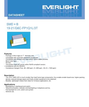
1. Product Overview
The 19-21 SMD LED is a compact, surface-mount device designed for modern electronic applications requiring high-density component placement. This LED utilizes an AlGaInP (Aluminum Gallium Indium Phosphide) chip to produce a Brilliant Yellow-Green light output, encapsulated in a water-clear resin package. Its primary advantage lies in its significantly reduced footprint compared to traditional lead-frame LEDs, enabling more compact PCB designs, higher packing density, and ultimately smaller end-user equipment. The lightweight construction further makes it ideal for miniature and portable applications.
1.1 Core Features and Compliance
The device is supplied on 8mm tape mounted on 7-inch diameter reels, ensuring compatibility with standard automated pick-and-place assembly equipment. It is designed for use with both infrared and vapor phase reflow soldering processes. The product is a mono-color type, is lead-free (Pb-free), and is compliant with key environmental and safety regulations including RoHS, EU REACH, and halogen-free standards (Bromine <900 ppm, Chlorine <900 ppm, Br+Cl < 1500 ppm).
1.2 Target Applications
This LED is suited for a variety of illumination and indication purposes. Common applications include backlighting for instrument panels, switches, and symbols; status indicators and keypad backlighting in telecommunication devices such as phones and fax machines; flat backlighting for LCD displays; and general-purpose indicator use where a bright, reliable light source is required.
2. Technical Specifications Deep Dive
This section provides a detailed, objective analysis of the device's electrical, optical, and thermal parameters as defined in the absolute maximum ratings and electro-optical characteristics tables.
2.1 Absolute Maximum Ratings
The absolute maximum ratings define the stress limits beyond which permanent damage to the device may occur. These are not recommended operating conditions.
- Reverse Voltage (VR): 5V. Exceeding this voltage in reverse bias can cause junction breakdown.
- Forward Current (IF): 25 mA (continuous).
- Peak Forward Current (IFP): 60 mA, permissible only under pulsed conditions (duty cycle 1/10 @ 1kHz).
- Power Dissipation (Pd): 60 mW. This is the maximum allowable power the package can dissipate as heat, calculated as VF * IF.
- Electrostatic Discharge (ESD) HBM: 2000V. This Human Body Model rating indicates a moderate level of ESD sensitivity; proper handling procedures are necessary.
- Operating Temperature (Topr): -40°C to +85°C. The device is rated for industrial temperature ranges.
- Storage Temperature (Tstg): -40°C to +90°C.
- Soldering Temperature (Tsol): Reflow profile peak at 260°C for max 10 seconds; hand soldering iron tip temperature <350°C for max 3 seconds per terminal.
2.2 Electro-Optical Characteristics
Measured at a standard test condition of 25°C ambient temperature and a forward current (IF) of 20 mA, unless otherwise specified.
- Luminous Intensity (Iv): Ranges from 45.0 mcd (min) to 90.0 mcd (max), with a typical tolerance of ±11%. This parameter defines the perceived brightness of the LED.
- Viewing Angle (2θ1/2): Approximately 100 degrees (typical). This wide viewing angle is characteristic of the water-clear dome lens, providing a broad emission pattern.
- Peak Wavelength (λp): Typically 575 nm. This is the wavelength at which the spectral power distribution is maximum.
- Dominant Wavelength (λd): Ranges from 570.0 nm to 574.5 nm, with a tolerance of ±1 nm. This is the single wavelength perceived by the human eye, defining the color (yellow-green).
- Spectral Bandwidth (Δλ): Typically 20 nm. This indicates the spectral purity of the emitted light.
- Forward Voltage (VF): Ranges from 1.70 V to 2.30 V at IF=20mA, with a tolerance of ±0.05V. This is the voltage drop across the LED when conducting current.
- Reverse Current (IR): Maximum 10 μA at VR=5V. The device is not designed for operation in reverse bias; this parameter is for leakage current testing only.
3. Binning System Explanation
The product is classified into bins based on three key parameters: Luminous Intensity, Dominant Wavelength, and Forward Voltage. This binning ensures consistency within a production lot and allows designers to select LEDs matching specific performance criteria.
3.1 Luminous Intensity Binning
Binned at IF = 20 mA. The bin codes (P1, P2, Q1) categorize the minimum and maximum luminous intensity values.
- P1: 45.0 - 57.0 mcd
- P2: 57.0 - 72.0 mcd
- Q1: 72.0 - 90.0 mcd
3.2 Dominant Wavelength Binning
Binned at IF = 20 mA. The bin codes (CC2, CC3, CC4) define narrow ranges of dominant wavelength to control color consistency.
- CC2: 570.0 - 571.5 nm
- CC3: 571.5 - 573.0 nm
- CC4: 573.0 - 574.5 nm
3.3 Forward Voltage Binning
Binned at IF = 20 mA. The bin codes (19, 20, 21, 22, 23, 24) categorize the forward voltage drop in 0.1V steps. This is critical for designing current-limiting resistor networks, especially when multiple LEDs are connected in series, to ensure uniform current distribution.
- 19: 1.70 - 1.80 V
- 20: 1.80 - 1.90 V
- 21: 1.90 - 2.00 V
- 22: 2.00 - 2.10 V
- 23: 2.10 - 2.20 V
- 24: 2.20 - 2.30 V
The part number "19-21/G6C-FP1Q1L/3T" incorporates specific bin codes, indicating the shipped product's performance within these defined ranges.
4. Performance Curve Analysis
While specific graphical data is referenced in the datasheet, typical performance trends for AlGaInP LEDs can be inferred and are crucial for design.
4.1 Forward Current vs. Forward Voltage (I-V Curve)
The forward voltage (VF) exhibits a logarithmic relationship with forward current (IF). A small increase in applied voltage beyond the turn-on threshold (~1.7V) results in a large, potentially damaging increase in current. This underscores the critical need for a constant current driver or a current-limiting resistor in series with the LED.
4.2 Temperature Dependence
Key parameters are temperature-dependent. Typically, the forward voltage (VF) decreases with increasing junction temperature (negative temperature coefficient). Conversely, luminous intensity generally decreases as temperature rises. Designers must account for these variations, especially in applications with wide ambient temperature swings or high internal heat generation.
4.3 Spectral Characteristics
The emitted spectrum is centered around 575 nm (yellow-green). The typical 20 nm spectral bandwidth indicates a relatively pure color emission. The dominant wavelength may shift slightly (usually towards longer wavelengths) with increased junction temperature and drive current.
5. Mechanical and Package Information
5.1 Package Dimensions
The 19-21 SMD LED features a compact rectangular package. Key dimensions (in mm, tolerance ±0.1mm unless specified) include a body length of 2.0 mm, width of 1.25 mm, and height of 0.8 mm. The detailed drawing specifies pad spacing and land pattern recommendations essential for PCB layout to ensure proper soldering and mechanical stability.
5.2 Polarity Identification
The cathode is clearly marked on the package. Correct polarity orientation is mandatory during assembly, as applying reverse voltage exceeding 5V can instantly destroy the device.
6. Soldering and Assembly Guidelines
Adherence to these guidelines is critical for reliability and preventing damage during the manufacturing process.
6.1 Reflow Soldering Profile
A lead-free (Pb-free) reflow profile is specified:
- Pre-heating: 150-200°C for 60-120 seconds.
- Time Above Liquidus (217°C): 60-150 seconds.
- Peak Temperature: Maximum 260°C.
- Time at Peak: Maximum 10 seconds.
- Heating Rate: Maximum 6°C/sec.
- Time Above 255°C: Maximum 30 seconds.
- Cooling Rate: Maximum 3°C/sec.
6.2 Hand Soldering
If hand soldering is unavoidable, use a soldering iron with a tip temperature less than 350°C. Contact time per terminal must not exceed 3 seconds. Use a low-power iron (<25W) and allow a cooling interval of at least 2 seconds between soldering each terminal to prevent thermal shock.
6.3 Storage and Moisture Sensitivity
The LEDs are packaged in a moisture-resistant barrier bag with desiccant.
- Do not open the bag until ready for use.
- After opening, unused LEDs must be stored at ≤30°C and ≤60% Relative Humidity.
- The "floor life" after bag opening is 168 hours (7 days).
- If the exposure time is exceeded or the desiccant indicator shows saturation, a baking treatment of 60°C ±5°C for 24 hours is required before reflow soldering.
7. Packaging and Ordering Information
7.1 Reel and Tape Specifications
The device is supplied in embossed carrier tape on 7-inch diameter reels. Standard loaded quantity is 3000 pieces per reel. The reel, tape, and cover tape dimensions are provided to ensure compatibility with automated feeders.
7.2 Label Explanation
The reel label contains critical information for traceability and verification:
- CPN: Customer's Product Number.
- P/N: Manufacturer's Product Number (e.g., 19-21/G6C-FP1Q1L/3T).
- QTY: Packing Quantity.
- CAT: Luminous Intensity Rank (Bin Code).
- HUE: Chromaticity Coordinates & Dominant Wavelength Rank (Bin Code).
- REF: Forward Voltage Rank (Bin Code).
- LOT No: Manufacturing Lot Number for traceability.
8. Application Design Considerations
8.1 Current Limiting is Mandatory
An external current-limiting mechanism is absolutely required. The simplest method is a series resistor. The resistor value (Rs) can be calculated using Ohm's Law: Rs = (Vsupply - VF) / IF. Use the maximum VF from the bin or datasheet to ensure IF does not exceed 25 mA under worst-case conditions. For precision or stability, a constant current driver circuit is recommended.
8.2 Thermal Management
While the package is small, effective heat sinking through the PCB pads is important for maintaining performance and longevity, especially when operating near maximum ratings. Ensure the PCB layout provides adequate copper area around the LED pads to act as a heat spreader.
8.3 ESD Protection
With an ESD HBM rating of 2000V, the device has moderate sensitivity. Implement standard ESD precautions during handling, assembly, and in the circuit design if the LED is connected to external interfaces.
9. Technical Comparison and Differentiation
The 19-21 LED differentiates itself primarily through its compact 2.0x1.25mm footprint, which is smaller than many traditional SMD LEDs like the 0603 or 0805 sizes, allowing for higher density layouts. The use of AlGaInP technology provides high efficiency and bright output in the yellow-green spectrum. The wide 100-degree viewing angle from the water-clear lens offers broad, even illumination compared to devices with diffused or narrow-angle lenses. Its compliance with halogen-free and other environmental standards makes it suitable for modern eco-conscious designs.
10. Frequently Asked Questions (FAQ)
10.1 What resistor value should I use with a 5V supply?
Using the maximum VF of 2.30V (Bin 24) and a target IF of 20 mA: R = (5V - 2.30V) / 0.020A = 135 Ohms. The nearest standard higher value (e.g., 150 Ohms) would be a safe choice, resulting in IF ≈ 18 mA. Always verify with actual VF of your specific bin.
10.2 Can I drive this LED without a resistor using a constant voltage source?
No. The negative temperature coefficient of VF can lead to thermal runaway. A slight increase in temperature lowers VF, which in turn increases current if driven by a constant voltage, causing further heating and potentially catastrophic failure. Always use a current-limiting scheme.
10.3 How do I interpret the part number 19-21/G6C-FP1Q1L/3T?
The "19-21" denotes the package family and size. The subsequent codes (G6C, FP1Q1L, 3T) are internal binning and product codes specifying the luminous intensity, dominant wavelength, and forward voltage characteristics as per the bin tables provided in the datasheet.
10.4 Is this LED suitable for automotive interior lighting?
While it may be used in some non-critical interior applications (like switch backlighting), the datasheet includes an application restriction note. For high-reliability automotive safety/security systems (e.g., dashboard warning lights), medical equipment, or military/aerospace applications, a product specifically qualified for those harsh environments should be sourced. Always verify suitability for the intended use case.
11. Practical Design Case Study
Scenario: Designing a status indicator panel with 10 uniformly bright yellow-green LEDs powered from a 3.3V rail.
Design Steps:
- Current Selection: Choose IF = 15 mA for a balance of brightness and power consumption.
- Voltage Bin Consideration: To ensure uniform brightness, specify LEDs from the same or adjacent VF bins (e.g., Bin 20: 1.80-1.90V). Using the max VF of 1.90V for calculation ensures all LEDs will light even with worst-case variation.
- Resistor Calculation: Rs = (3.3V - 1.90V) / 0.015A ≈ 93.3 Ohms. Use a standard 100 Ohm resistor. Actual IF will range from ~14 mA (for a 1.90V LED) to ~15.6 mA (for a 1.75V LED, assuming a lower bin), providing acceptable uniformity.
- PCB Layout: Place each LED with its 100Ω series resistor close to its anode pad. Provide a small copper pour connected to the cathode pads for minor heat dissipation.
- Assembly: Follow the specified reflow profile. Keep the bag sealed until the production line is ready, and complete soldering within the 7-day floor life after opening.
12. Operating Principle
The LED operates on the principle of electroluminescence in a semiconductor p-n junction. The active region is composed of AlGaInP (Aluminum Gallium Indium Phosphide) semiconductor materials. When a forward bias voltage exceeding the junction's built-in potential is applied, electrons from the n-type region and holes from the p-type region are injected into the active region. There, they recombine radiatively, releasing energy in the form of photons. The specific bandgap energy of the AlGaInP alloy determines the wavelength of the emitted light, which in this case is in the yellow-green portion of the visible spectrum (around 575 nm). The water-clear epoxy resin encapsulant acts as a lens, shaping the light output and providing mechanical and environmental protection for the semiconductor chip.
13. Technology Trends
The general trend in SMD LEDs like the 19-21 is towards continued miniaturization, increased luminous efficacy (more light output per electrical watt), and higher reliability. There is also a strong drive for broader adoption of environmentally friendly materials and manufacturing processes, as evidenced by this product's compliance with RoHS, REACH, and halogen-free standards. In terms of packaging, advancements aim to improve thermal management from the chip to the PCB to support higher drive currents in smaller footprints. Color consistency and tighter binning tolerances are also areas of ongoing development to meet the demands of applications requiring precise color matching.
LED Specification Terminology
Complete explanation of LED technical terms
Photoelectric Performance
| Term | Unit/Representation | Simple Explanation | Why Important |
|---|---|---|---|
| Luminous Efficacy | lm/W (lumens per watt) | Light output per watt of electricity, higher means more energy efficient. | Directly determines energy efficiency grade and electricity cost. |
| Luminous Flux | lm (lumens) | Total light emitted by source, commonly called "brightness". | Determines if the light is bright enough. |
| Viewing Angle | ° (degrees), e.g., 120° | Angle where light intensity drops to half, determines beam width. | Affects illumination range and uniformity. |
| CCT (Color Temperature) | K (Kelvin), e.g., 2700K/6500K | Warmth/coolness of light, lower values yellowish/warm, higher whitish/cool. | Determines lighting atmosphere and suitable scenarios. |
| CRI / Ra | Unitless, 0–100 | Ability to render object colors accurately, Ra≥80 is good. | Affects color authenticity, used in high-demand places like malls, museums. |
| SDCM | MacAdam ellipse steps, e.g., "5-step" | Color consistency metric, smaller steps mean more consistent color. | Ensures uniform color across same batch of LEDs. |
| Dominant Wavelength | nm (nanometers), e.g., 620nm (red) | Wavelength corresponding to color of colored LEDs. | Determines hue of red, yellow, green monochrome LEDs. |
| Spectral Distribution | Wavelength vs intensity curve | Shows intensity distribution across wavelengths. | Affects color rendering and quality. |
Electrical Parameters
| Term | Symbol | Simple Explanation | Design Considerations |
|---|---|---|---|
| Forward Voltage | Vf | Minimum voltage to turn on LED, like "starting threshold". | Driver voltage must be ≥Vf, voltages add up for series LEDs. |
| Forward Current | If | Current value for normal LED operation. | Usually constant current drive, current determines brightness & lifespan. |
| Max Pulse Current | Ifp | Peak current tolerable for short periods, used for dimming or flashing. | Pulse width & duty cycle must be strictly controlled to avoid damage. |
| Reverse Voltage | Vr | Max reverse voltage LED can withstand, beyond may cause breakdown. | Circuit must prevent reverse connection or voltage spikes. |
| Thermal Resistance | Rth (°C/W) | Resistance to heat transfer from chip to solder, lower is better. | High thermal resistance requires stronger heat dissipation. |
| ESD Immunity | V (HBM), e.g., 1000V | Ability to withstand electrostatic discharge, higher means less vulnerable. | Anti-static measures needed in production, especially for sensitive LEDs. |
Thermal Management & Reliability
| Term | Key Metric | Simple Explanation | Impact |
|---|---|---|---|
| Junction Temperature | Tj (°C) | Actual operating temperature inside LED chip. | Every 10°C reduction may double lifespan; too high causes light decay, color shift. |
| Lumen Depreciation | L70 / L80 (hours) | Time for brightness to drop to 70% or 80% of initial. | Directly defines LED "service life". |
| Lumen Maintenance | % (e.g., 70%) | Percentage of brightness retained after time. | Indicates brightness retention over long-term use. |
| Color Shift | Δu′v′ or MacAdam ellipse | Degree of color change during use. | Affects color consistency in lighting scenes. |
| Thermal Aging | Material degradation | Deterioration due to long-term high temperature. | May cause brightness drop, color change, or open-circuit failure. |
Packaging & Materials
| Term | Common Types | Simple Explanation | Features & Applications |
|---|---|---|---|
| Package Type | EMC, PPA, Ceramic | Housing material protecting chip, providing optical/thermal interface. | EMC: good heat resistance, low cost; Ceramic: better heat dissipation, longer life. |
| Chip Structure | Front, Flip Chip | Chip electrode arrangement. | Flip chip: better heat dissipation, higher efficacy, for high-power. |
| Phosphor Coating | YAG, Silicate, Nitride | Covers blue chip, converts some to yellow/red, mixes to white. | Different phosphors affect efficacy, CCT, and CRI. |
| Lens/Optics | Flat, Microlens, TIR | Optical structure on surface controlling light distribution. | Determines viewing angle and light distribution curve. |
Quality Control & Binning
| Term | Binning Content | Simple Explanation | Purpose |
|---|---|---|---|
| Luminous Flux Bin | Code e.g., 2G, 2H | Grouped by brightness, each group has min/max lumen values. | Ensures uniform brightness in same batch. |
| Voltage Bin | Code e.g., 6W, 6X | Grouped by forward voltage range. | Facilitates driver matching, improves system efficiency. |
| Color Bin | 5-step MacAdam ellipse | Grouped by color coordinates, ensuring tight range. | Guarantees color consistency, avoids uneven color within fixture. |
| CCT Bin | 2700K, 3000K etc. | Grouped by CCT, each has corresponding coordinate range. | Meets different scene CCT requirements. |
Testing & Certification
| Term | Standard/Test | Simple Explanation | Significance |
|---|---|---|---|
| LM-80 | Lumen maintenance test | Long-term lighting at constant temperature, recording brightness decay. | Used to estimate LED life (with TM-21). |
| TM-21 | Life estimation standard | Estimates life under actual conditions based on LM-80 data. | Provides scientific life prediction. |
| IESNA | Illuminating Engineering Society | Covers optical, electrical, thermal test methods. | Industry-recognized test basis. |
| RoHS / REACH | Environmental certification | Ensures no harmful substances (lead, mercury). | Market access requirement internationally. |
| ENERGY STAR / DLC | Energy efficiency certification | Energy efficiency and performance certification for lighting. | Used in government procurement, subsidy programs, enhances competitiveness. |