Table of Contents
- 1. Product Overview
- 1.1 Core Advantages and Product Positioning
- 1.2 Target Market and Applications
- 2. In-Depth Technical Parameter Analysis
- 2.1 Absolute Maximum Ratings
- 2.2 Electro-Optical Characteristics
- 3. Binning System Explanation
- 3.1 Luminous Intensity Binning
- 3.2 Dominant Wavelength Binning
- 4. Performance Curve Analysis
- 5. Mechanical and Package Information
- 5.1 Package Dimensions and Polarity
- 5.2 Tape and Reel Packaging
- 6. Soldering and Assembly Guidelines
- 6.1 Storage and Moisture Sensitivity
- 6.2 Reflow Soldering Profile
- 6.3 Hand Soldering and Rework
- 7. Application Design Considerations
- 7.1 Circuit Design
- 7.2 Thermal Management
- 7.3 Application Restrictions
- 8. Technical Comparison and Differentiation
- 9. Frequently Asked Questions (FAQ)
- 10. Practical Design and Usage Case
- 11. Operating Principle Introduction
- 12. Technology Trends and Context
- LED Specification Terminology
- Photoelectric Performance
- Electrical Parameters
- Thermal Management & Reliability
- Packaging & Materials
- Quality Control & Binning
- Testing & Certification
1. Product Overview
This document details the specifications for a compact, high-performance Surface-Mount Device (SMD) Light Emitting Diode (LED) in a 1206 package format, emitting blue light. The component is designed for modern, automated electronics assembly processes, offering significant advantages in board space utilization and design flexibility for a wide range of indicator and backlighting applications.
1.1 Core Advantages and Product Positioning
The primary advantage of this LED is its miniature footprint, which is significantly smaller than traditional lead-frame type components. This reduction in size enables designers to achieve smaller printed circuit board (PCB) layouts, higher component packing density, and ultimately, more compact end-user equipment. Its lightweight construction further makes it ideal for applications where weight and space are critical constraints. The product is positioned as a reliable, RoHS-compliant, and halogen-free solution for general-purpose lighting and indication needs across consumer and industrial electronics.
1.2 Target Market and Applications
This LED is suited for a broad spectrum of applications requiring a compact, bright blue indicator. Key application areas include:
- Backlighting: Illumination for instrument panel dashboards, membrane switches, and control panels.
- Telecommunications Equipment: Status indicators and keypad backlighting in telephones, fax machines, and other communication devices.
- Display Technology: Providing flat, uniform backlighting for liquid crystal displays (LCDs), switch legends, and symbols.
- General Purpose Indication: Any application requiring a small, efficient, and bright blue light source for status, power, or functional indication.
2. In-Depth Technical Parameter Analysis
The performance of the LED is defined by a set of absolute maximum ratings and standard operating characteristics. Understanding these parameters is crucial for reliable circuit design and ensuring long-term product longevity.
2.1 Absolute Maximum Ratings
These ratings define the stress limits beyond which permanent damage to the device may occur. Operation under or at these limits is not guaranteed and should be avoided in normal use.
- Reverse Voltage (VR): 5 V. Exceeding this voltage in reverse bias can cause junction breakdown.
- Continuous Forward Current (IF): 20 mA. This is the recommended maximum current for continuous DC operation.
- Peak Forward Current (IFP): 100 mA. This higher current is permissible only under pulsed conditions (duty cycle 1/10 at 1 kHz) and must not be used for DC operation.
- Power Dissipation (Pd): 75 mW. This is the maximum power the package can dissipate, calculated as Forward Voltage (VF) multiplied by Forward Current (IF).
- Operating Temperature (Topr): -40°C to +85°C. The ambient temperature range for reliable operation.
- Storage Temperature (Tstg): -40°C to +90°C.
- Soldering Temperature: The device can withstand reflow soldering with a peak temperature of 260°C for up to 10 seconds, or hand soldering at 350°C for up to 3 seconds per terminal.
2.2 Electro-Optical Characteristics
These parameters are measured at a standard junction temperature of 25°C with a forward current of 20 mA, representing typical performance.
- Luminous Intensity (Iv): Ranges from a minimum of 45.0 mcd to a maximum of 112.0 mcd. The actual value is binned (see Section 3).
- Viewing Angle (2θ1/2): Approximately 130 degrees. This wide viewing angle makes the LED suitable for applications where visibility from off-axis angles is important.
- Peak Wavelength (λp): Typically 468 nm. This is the wavelength at which the spectral output is strongest.
- Dominant Wavelength (λd): Ranges from 464.5 nm to 476.5 nm. This is the wavelength perceived by the human eye and is also binned.
- Spectral Bandwidth (Δλ): Typically 25 nm, measured at half the maximum intensity (Full Width at Half Maximum - FWHM).
- Forward Voltage (VF): Typically 3.3V, with a range from 2.7V to 3.7V at 20mA. A current-limiting resistor is mandatory in series with the LED to prevent thermal runaway.
- Reverse Current (IR): Maximum of 50 μA when a 5V reverse bias is applied. The datasheet explicitly warns that reverse voltage operation is for test purposes only and should not be used in circuit design.
3. Binning System Explanation
To ensure consistency in mass production, LEDs are sorted into performance bins based on key parameters. This allows designers to select parts that meet specific brightness and color requirements.
3.1 Luminous Intensity Binning
The luminous output is categorized into four distinct bins (P1, P2, Q1, Q2), each defining a minimum and maximum intensity range measured at IF = 20 mA. The total tolerance for luminous intensity is ±11%.
- P1: 45.0 - 57.0 mcd
- P2: 57.0 - 72.0 mcd
- Q1: 72.0 - 90.0 mcd
- Q2: 90.0 - 112.0 mcd
3.2 Dominant Wavelength Binning
The color (hue) of the blue light is controlled by binning the dominant wavelength into four codes (A9, A10, A11, A12), with a tight tolerance of ±1 nm.
- A9: 464.5 - 467.5 nm
- A10: 467.5 - 470.5 nm
- A11: 470.5 - 473.5 nm
- A12: 473.5 - 476.5 nm
This binning allows for precise color matching in applications where multiple LEDs are used adjacent to each other.
4. Performance Curve Analysis
While the datasheet references typical electro-optical characteristic curves, the provided tables give critical insight. The relationship between forward current (IF) and forward voltage (VF) is non-linear and exponential in nature. A small increase in voltage beyond the typical VF can lead to a large, potentially destructive increase in current. This underscores the critical importance of using a series current-limiting resistor in the driving circuit. The luminous intensity is directly proportional to the forward current, but this relationship also depends on junction temperature, which rises with increased power dissipation.
5. Mechanical and Package Information
5.1 Package Dimensions and Polarity
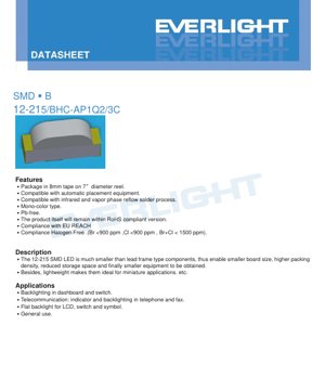
The LED conforms to the standard 1206 (Imperial 3216 metric) package footprint. Key dimensions include a body length of 1.6 mm, a width of 0.8 mm, and a height of 0.7 mm. Polarity is clearly marked: the cathode terminal is identified by a green marking on the top of the component and a distinctive notch or chamfer on one end of the package. Correct orientation during placement is essential for proper circuit function.
5.2 Tape and Reel Packaging
The components are supplied in moisture-resistant packaging, mounted on 8mm wide carrier tape and wound onto 7-inch diameter reels. Each reel contains 3000 pieces. The packaging includes a desiccant and is sealed within an aluminum moisture-proof bag to protect the LEDs from ambient humidity during storage and transport, which is critical for preventing "popcorning" or delamination during the high-temperature reflow soldering process.
6. Soldering and Assembly Guidelines
Proper handling is required to maintain device reliability.
6.1 Storage and Moisture Sensitivity
This LED is moisture-sensitive. The unopened bag must be stored at ≤30°C and ≤90% RH. Once opened, the components have a "floor life" of 168 hours (7 days) under conditions of ≤30°C and ≤60% RH. If not used within this time, or if the desiccant indicator has changed color, the LEDs must be rebaked at 60°C ±5°C for 24 hours before being subjected to reflow soldering.
6.2 Reflow Soldering Profile
A lead-free (Pb-free) reflow profile is specified:
- Pre-heating: 150-200°C for 60-120 seconds.
- Time Above Liquidus (TAL): 60-150 seconds above 217°C.
- Peak Temperature: Maximum of 260°C, held for no more than 10 seconds.
- Ramp Rates: Maximum heating rate of 6°C/sec and maximum cooling rate of 3°C/sec.
Reflow soldering should not be performed more than two times. Stress on the LED body during heating and warping of the PCB after soldering must be avoided.
6.3 Hand Soldering and Rework
If hand soldering is necessary, it should be performed with a soldering iron tip temperature below 350°C, applied for no more than 3 seconds per terminal, using an iron with a power rating of 25W or less. A cooling interval of at least 2 seconds should be allowed between soldering each terminal. Rework after initial soldering is strongly discouraged. If absolutely unavoidable, a specialized double-head soldering iron must be used to simultaneously heat both terminals, preventing mechanical stress on the solder joints and the LED package.
7. Application Design Considerations
7.1 Circuit Design
The most critical design rule is the mandatory use of a series current-limiting resistor. The LED's exponential I-V characteristic means it does not self-regulate current like a resistor. Connecting it directly to a voltage source will cause excessive current flow, leading to immediate failure. The resistor value (R) is calculated using Ohm's Law: R = (Vsupply - VF) / IF, where VF is the typical or maximum forward voltage from the datasheet, and IF is the desired operating current (≤20 mA).
7.2 Thermal Management
Although the power dissipation is low (75 mW maximum), proper PCB layout can enhance longevity. Ensuring adequate copper area around the LED's thermal pads (the solder joints themselves) helps dissipate heat from the junction. Operating the LED at lower currents than the maximum rating, or using pulsed operation, can significantly extend its lifespan and maintain luminous output.
7.3 Application Restrictions
The datasheet includes a clear disclaimer that this product, as specified, may not be suitable for high-reliability applications with severe consequences of failure, such as military/aerospace systems, automotive safety systems (e.g., airbags, braking), or life-critical medical equipment. For such applications, components with different qualifications, testing, and specifications are required.
8. Technical Comparison and Differentiation
Compared to larger through-hole LEDs, this SMD component offers a drastic reduction in size and weight, enabling modern miniaturized electronics. Within the SMD LED family, the 1206 package represents a common and cost-effective size, balancing ease of manual handling (for prototyping) with suitability for automated pick-and-place machines. Its wide 130-degree viewing angle is a key differentiator from narrower-angle LEDs, making it preferable for applications where the indicator needs to be seen from a wide range of positions. The specified compliance with RoHS, REACH, and halogen-free standards ensures it meets stringent international environmental regulations.
9. Frequently Asked Questions (FAQ)
Q: Why is a current-limiting resistor absolutely necessary?
A: An LED has a very low dynamic resistance in its forward-biased region. Without a resistor to limit current, even a small voltage source will drive a current far exceeding the LED's maximum rating, causing instantaneous thermal overload and destruction.
Q: Can I drive this LED with a 5V supply?
A: Yes, but you must use a series resistor. For example, targeting IF = 20mA with a typical VF of 3.3V: R = (5V - 3.3V) / 0.020A = 85 Ohms. A standard 82 Ohm or 100 Ohm resistor would be appropriate, resulting in a slightly lower or higher current, respectively.
Q: What do the bin codes (e.g., Q2, A11) on the reel label mean?
A: They specify the performance group of the LEDs on that reel. "Q2" indicates the luminous intensity bin (90.0-112.0 mcd). "A11" indicates the dominant wavelength bin (470.5-473.5 nm). Specifying bins allows for consistency in brightness and color across a production run.
Q: How critical are the moisture sensitivity warnings?
A> Very critical. Absorbed moisture can vaporize during the high-temperature reflow soldering process, creating internal pressure that can crack the LED's epoxy resin package or delaminate it from the internal die, leading to immediate or latent failure.
10. Practical Design and Usage Case
Scenario: Designing a multi-LED status panel. A designer is creating a control panel with ten blue status indicators. To ensure uniform appearance, they specify LEDs from the same luminous intensity bin (e.g., all Q1) and the same dominant wavelength bin (e.g., all A10) in their Bill of Materials (BOM). They plan to drive each LED from a 3.3V microcontroller GPIO pin. Calculating the resistor: R = (3.3V - 3.3V) / 0.020A = 0 Ohms. This is invalid, as there is no voltage drop across the resistor. Therefore, they must either use a lower current (e.g., 10mA) or drive the LEDs from a higher voltage rail (e.g., 5V) with an appropriate resistor. They choose a 5V rail. Using the maximum VF of 3.7V for a conservative design: R = (5V - 3.7V) / 0.020A = 65 Ohms. They select a standard 68 Ohm, 1/10W resistor for each LED. They ensure the PCB layout provides a small amount of copper pour around the LED pads for heat dissipation and follow the recommended reflow profile during assembly.
11. Operating Principle Introduction
This LED is based on an Indium Gallium Nitride (InGaN) semiconductor chip. When a forward voltage exceeding the diode's built-in potential is applied, electrons and holes are injected into the active region of the semiconductor junction. When these charge carriers recombine, they release energy in the form of photons (light). The specific composition of the InGaN alloy determines the bandgap energy, which in turn dictates the wavelength (color) of the emitted light—in this case, blue. The chip is encapsulated in a clear epoxy resin that protects the semiconductor, acts as a lens to shape the light output (creating the 130-degree viewing angle), and provides the mechanical structure of the 1206 package.
12. Technology Trends and Context
The component described represents a mature and widely adopted technology. The trend in SMD LEDs continues toward even smaller packages (e.g., 0805, 0603, 0402) for ultra-miniaturization, as well as toward higher-power packages for illumination. There is also a strong trend toward improved efficiency (more lumens per watt), which reduces power consumption and heat generation for a given light output. Furthermore, the precision and consistency of binning processes have improved significantly, allowing for tighter color and brightness tolerances in mass production, which is essential for applications like full-color displays and architectural lighting where color uniformity is paramount.
LED Specification Terminology
Complete explanation of LED technical terms
Photoelectric Performance
| Term | Unit/Representation | Simple Explanation | Why Important |
|---|---|---|---|
| Luminous Efficacy | lm/W (lumens per watt) | Light output per watt of electricity, higher means more energy efficient. | Directly determines energy efficiency grade and electricity cost. |
| Luminous Flux | lm (lumens) | Total light emitted by source, commonly called "brightness". | Determines if the light is bright enough. |
| Viewing Angle | ° (degrees), e.g., 120° | Angle where light intensity drops to half, determines beam width. | Affects illumination range and uniformity. |
| CCT (Color Temperature) | K (Kelvin), e.g., 2700K/6500K | Warmth/coolness of light, lower values yellowish/warm, higher whitish/cool. | Determines lighting atmosphere and suitable scenarios. |
| CRI / Ra | Unitless, 0–100 | Ability to render object colors accurately, Ra≥80 is good. | Affects color authenticity, used in high-demand places like malls, museums. |
| SDCM | MacAdam ellipse steps, e.g., "5-step" | Color consistency metric, smaller steps mean more consistent color. | Ensures uniform color across same batch of LEDs. |
| Dominant Wavelength | nm (nanometers), e.g., 620nm (red) | Wavelength corresponding to color of colored LEDs. | Determines hue of red, yellow, green monochrome LEDs. |
| Spectral Distribution | Wavelength vs intensity curve | Shows intensity distribution across wavelengths. | Affects color rendering and quality. |
Electrical Parameters
| Term | Symbol | Simple Explanation | Design Considerations |
|---|---|---|---|
| Forward Voltage | Vf | Minimum voltage to turn on LED, like "starting threshold". | Driver voltage must be ≥Vf, voltages add up for series LEDs. |
| Forward Current | If | Current value for normal LED operation. | Usually constant current drive, current determines brightness & lifespan. |
| Max Pulse Current | Ifp | Peak current tolerable for short periods, used for dimming or flashing. | Pulse width & duty cycle must be strictly controlled to avoid damage. |
| Reverse Voltage | Vr | Max reverse voltage LED can withstand, beyond may cause breakdown. | Circuit must prevent reverse connection or voltage spikes. |
| Thermal Resistance | Rth (°C/W) | Resistance to heat transfer from chip to solder, lower is better. | High thermal resistance requires stronger heat dissipation. |
| ESD Immunity | V (HBM), e.g., 1000V | Ability to withstand electrostatic discharge, higher means less vulnerable. | Anti-static measures needed in production, especially for sensitive LEDs. |
Thermal Management & Reliability
| Term | Key Metric | Simple Explanation | Impact |
|---|---|---|---|
| Junction Temperature | Tj (°C) | Actual operating temperature inside LED chip. | Every 10°C reduction may double lifespan; too high causes light decay, color shift. |
| Lumen Depreciation | L70 / L80 (hours) | Time for brightness to drop to 70% or 80% of initial. | Directly defines LED "service life". |
| Lumen Maintenance | % (e.g., 70%) | Percentage of brightness retained after time. | Indicates brightness retention over long-term use. |
| Color Shift | Δu′v′ or MacAdam ellipse | Degree of color change during use. | Affects color consistency in lighting scenes. |
| Thermal Aging | Material degradation | Deterioration due to long-term high temperature. | May cause brightness drop, color change, or open-circuit failure. |
Packaging & Materials
| Term | Common Types | Simple Explanation | Features & Applications |
|---|---|---|---|
| Package Type | EMC, PPA, Ceramic | Housing material protecting chip, providing optical/thermal interface. | EMC: good heat resistance, low cost; Ceramic: better heat dissipation, longer life. |
| Chip Structure | Front, Flip Chip | Chip electrode arrangement. | Flip chip: better heat dissipation, higher efficacy, for high-power. |
| Phosphor Coating | YAG, Silicate, Nitride | Covers blue chip, converts some to yellow/red, mixes to white. | Different phosphors affect efficacy, CCT, and CRI. |
| Lens/Optics | Flat, Microlens, TIR | Optical structure on surface controlling light distribution. | Determines viewing angle and light distribution curve. |
Quality Control & Binning
| Term | Binning Content | Simple Explanation | Purpose |
|---|---|---|---|
| Luminous Flux Bin | Code e.g., 2G, 2H | Grouped by brightness, each group has min/max lumen values. | Ensures uniform brightness in same batch. |
| Voltage Bin | Code e.g., 6W, 6X | Grouped by forward voltage range. | Facilitates driver matching, improves system efficiency. |
| Color Bin | 5-step MacAdam ellipse | Grouped by color coordinates, ensuring tight range. | Guarantees color consistency, avoids uneven color within fixture. |
| CCT Bin | 2700K, 3000K etc. | Grouped by CCT, each has corresponding coordinate range. | Meets different scene CCT requirements. |
Testing & Certification
| Term | Standard/Test | Simple Explanation | Significance |
|---|---|---|---|
| LM-80 | Lumen maintenance test | Long-term lighting at constant temperature, recording brightness decay. | Used to estimate LED life (with TM-21). |
| TM-21 | Life estimation standard | Estimates life under actual conditions based on LM-80 data. | Provides scientific life prediction. |
| IESNA | Illuminating Engineering Society | Covers optical, electrical, thermal test methods. | Industry-recognized test basis. |
| RoHS / REACH | Environmental certification | Ensures no harmful substances (lead, mercury). | Market access requirement internationally. |
| ENERGY STAR / DLC | Energy efficiency certification | Energy efficiency and performance certification for lighting. | Used in government procurement, subsidy programs, enhances competitiveness. |