Table of Contents
- 1. Product Overview
- 2. Technical Parameter Deep Dive
- 2.1 Absolute Maximum Ratings
- 2.2 Electro-Optical Characteristics
- 3. Binning System Explanation
- 3.1 Luminous Intensity Binning
- 3.2 Dominant Wavelength Binning
- 3.3 Forward Voltage Binning
- 4. Performance Curve Analysis
- 4.1 Relative Luminous Intensity vs. Forward Current
- 4.2 Relative Luminous Intensity vs. Ambient Temperature
- 4.3 Forward Current Derating Curve
- 4.4 Forward Voltage vs. Forward Current
- 4.5 Spectrum Distribution
- 4.6 Radiation Diagram
- 5. Mechanical and Package Information
- 5.1 Package Dimensions
- 5.2 Polarity Identification
- 6. Soldering and Assembly Guidelines
- 6.1 Current Limiting Requirement
- 6.2 Reflow Soldering Profile
- 6.3 Hand Soldering
- 6.4 Storage and Moisture Sensitivity
- 6.5 Rework and Repair
- 7. Packaging and Ordering Information
- 7.1 Standard Packaging
- 7.2 Reel and Tape Dimensions
- 7.3 Label Information
- 8. Application Suggestions
- 8.1 Typical Application Scenarios
- 8.2 Design Considerations
- 9. Technical Comparison and Differentiation
- 10. Frequently Asked Questions (Based on Technical Parameters)
- 10.1 What resistor value should I use with a 5V supply?
- 10.2 Can I drive this LED at 30mA for more brightness?
- 10.3 Why is the storage and baking process so important?
- 10.4 How do I interpret the bin codes (e.g., Q1, X, 12) on my reel?
- 11. Practical Design and Usage Case
- 12. Operating Principle
- 13. Technology Trends
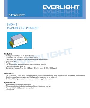
1. Product Overview
The 19-21 SMD LED is a compact, surface-mount device designed for modern electronic applications requiring reliable indicator or backlighting solutions. Its primary advantage lies in its significantly reduced footprint compared to traditional lead-frame LEDs, enabling higher component packing density on printed circuit boards (PCBs). This miniaturization contributes directly to smaller end-product designs, reduced storage requirements for components, and overall weight savings, making it ideal for space-constrained and portable devices.
The device is constructed using an InGaN (Indium Gallium Nitride) semiconductor chip, which emits blue light. The encapsulation is a water-clear resin, allowing for maximum light output. It is a mono-color type, supplied on 8mm tape mounted on 7-inch diameter reels for compatibility with high-speed automated pick-and-place assembly equipment. The product is fully compliant with lead-free (Pb-free) soldering processes, including infrared and vapor phase reflow. Furthermore, it adheres to key environmental and safety standards: it is within RoHS (Restriction of Hazardous Substances) compliant versions, complies with EU REACH regulations, and is Halogen-Free (with Bromine <900 ppm, Chlorine <900 ppm, and their sum <1500 ppm).
2. Technical Parameter Deep Dive
2.1 Absolute Maximum Ratings
These ratings define the limits beyond which permanent damage to the device may occur. Operation under or at these conditions is not guaranteed.
- Reverse Voltage (VR): 5V. Exceeding this voltage in reverse bias can cause junction breakdown.
- Forward Current (IF): 20mA (continuous). This is the recommended maximum current for reliable long-term operation.
- Peak Forward Current (IFP): 40mA, permissible only under pulsed conditions (duty cycle 1/10 at 1kHz).
- Power Dissipation (Pd): 75mW. This is the maximum power the package can dissipate without exceeding its thermal limits.
- Electrostatic Discharge (ESD): Human Body Model (HBM) rating of 150V. Proper ESD handling precautions are essential during assembly.
- Operating Temperature (Topr): -40°C to +85°C. The device is functional within this ambient temperature range.
- Storage Temperature (Tstg): -40°C to +90°C.
- Soldering Temperature (Tsol): Reflow profile peak at 260°C for a maximum of 10 seconds. Hand soldering iron tip temperature should not exceed 350°C for 3 seconds.
2.2 Electro-Optical Characteristics
These parameters are measured at a standard test condition of an ambient temperature (Ta) of 25°C and a forward current (IF) of 20mA, unless otherwise specified. They define the core light output and electrical performance.
- Luminous Intensity (Iv): Ranges from a minimum of 72.0 mcd to a maximum of 180.0 mcd. The typical value falls within this binning range (see Section 3).
- Viewing Angle (2θ1/2): Approximately 100 degrees. This is the full angle at which the luminous intensity is half of its peak value.
- Peak Wavelength (λp): Typically 468 nanometers (nm). This is the wavelength at which the spectral emission is strongest.
- Dominant Wavelength (λd): Ranges from 465.0 nm to 475.0 nm. This is the single wavelength perceived by the human eye, defining the color.
- Spectral Bandwidth (Δλ): Typically 25 nm. This measures the width of the emitted spectrum at half its maximum intensity.
- Forward Voltage (VF): Ranges from 2.70V to 3.70V at 20mA. This is the voltage drop across the LED when operating.
- Reverse Current (IR): Maximum of 50 μA when a reverse voltage of 5V is applied. The device is not designed for operation in reverse bias.
Important Notes: Tolerances are specified as ±11% for Luminous Intensity, ±1nm for Dominant Wavelength, and ±0.1V for Forward Voltage. The 5V reverse voltage condition is for testing IR only.
3. Binning System Explanation
To ensure consistent color and brightness in production applications, LEDs are sorted into bins based on key parameters. This allows designers to select parts that meet specific application requirements.
3.1 Luminous Intensity Binning
Binned at IF = 20mA. Codes indicate ascending brightness levels.
- Q1: 72.0 – 90.0 mcd
- Q2: 90.0 – 112.0 mcd
- R1: 112.0 – 140.0 mcd
- R2: 140.0 – 180.0 mcd
3.2 Dominant Wavelength Binning
Binned at IF = 20mA. Defines the precise shade of blue.
- X: 465.0 – 470.0 nm
- Y: 470.0 – 475.0 nm
3.3 Forward Voltage Binning
Binned at IF = 20mA. Important for designing current-limiting circuits and ensuring uniform brightness in parallel strings.
- 10: 2.70 – 2.90 V
- 11: 2.90 – 3.10 V
- 12: 3.10 – 3.30 V
- 13: 3.30 – 3.50 V
- 14: 3.50 – 3.70 V
4. Performance Curve Analysis
The datasheet provides several characteristic curves that are crucial for understanding the LED's behavior under different operating conditions.
4.1 Relative Luminous Intensity vs. Forward Current
This curve shows that light output increases with forward current but not linearly. It tends to saturate at higher currents. Operating significantly above the recommended 20mA may yield diminishing returns in brightness while increasing heat and accelerating degradation.
4.2 Relative Luminous Intensity vs. Ambient Temperature
LED efficiency decreases as junction temperature rises. This curve typically shows a gradual decline in light output as ambient temperature increases from -40°C to +85°C. Proper thermal management in the application is necessary to maintain consistent brightness.
4.3 Forward Current Derating Curve
This graph defines the maximum allowable continuous forward current as a function of ambient temperature. As temperature rises, the maximum permissible current must be reduced to stay within the device's power dissipation limits and prevent overheating.
4.4 Forward Voltage vs. Forward Current
This IV (Current-Voltage) characteristic is exponential in nature. A small change in forward voltage results in a large change in current, highlighting the critical need for a constant-current driver or a well-calculated series resistor.
4.5 Spectrum Distribution
The spectral plot shows a single peak centered around 468 nm, confirming the monochromatic blue output. The typical 25nm bandwidth indicates the spectral purity of the emitted light.
4.6 Radiation Diagram
This polar plot visually represents the viewing angle, showing the relative luminous intensity at different angles from the LED's central axis, confirming the approximately 100-degree viewing angle.
5. Mechanical and Package Information
5.1 Package Dimensions
The 19-21 SMD LED has a compact rectangular footprint. Key dimensions (in millimeters) are approximately 2.0mm in length, 1.25mm in width, and 0.8mm in height. Tolerances are typically ±0.1mm unless otherwise noted. The package features a cathode identification mark, which is essential for correct orientation during PCB assembly.
5.2 Polarity Identification
Correct polarity is mandatory for operation. The package includes a distinct cathode mark. Always refer to the package drawing to identify this mark on the physical component and align it with the corresponding marking on the PCB footprint.
6. Soldering and Assembly Guidelines
6.1 Current Limiting Requirement
Critical: An external current-limiting resistor or constant-current driver circuit MUST be used in series with the LED. The exponential IV characteristic means that a minor increase in supply voltage can cause a large, potentially destructive surge in forward current.
6.2 Reflow Soldering Profile
The device is suitable for lead-free reflow soldering. The recommended temperature profile is as follows:
- Pre-heating: 150–200°C for 60–120 seconds.
- Time Above Liquidus (217°C): 60–150 seconds.
- Peak Temperature: Maximum of 260°C.
- Time Within 5°C of Peak: Maximum of 10 seconds.
- Heating Rate: Maximum 3°C/second up to 217°C, then maximum 6°C/second to peak.
- Cooling Rate: Controlled cooling is recommended.
Note: Reflow soldering should not be performed more than two times on the same device.
6.3 Hand Soldering
If hand soldering is necessary, extreme care is required:
- Use a soldering iron with a tip temperature not exceeding 350°C.
- Limit contact time to a maximum of 3 seconds per terminal.
- Use an iron with a power rating of 25W or less.
- Allow a minimum of 2 seconds between soldering each terminal to avoid thermal stress.
6.4 Storage and Moisture Sensitivity
The components are packaged in a moisture-resistant barrier bag with desiccant.
- Do not open the bag until ready for use.
- After opening, unused LEDs should be stored at ≤30°C and ≤60% Relative Humidity.
- The "Floor Life" after bag opening is 168 hours (7 days).
- If components exceed this time or the desiccant indicator changes color, a bake-out is required: 60°C ±5°C for 24 hours before reflow.
6.5 Rework and Repair
Rework after soldering is strongly discouraged. If absolutely unavoidable, use a dual-head soldering iron to simultaneously heat both terminals and lift the component evenly to prevent mechanical stress on the solder joints or the LED package. Always verify device functionality after any rework.
7. Packaging and Ordering Information
7.1 Standard Packaging
The LEDs are supplied in embossed carrier tape on 7-inch diameter reels. Each reel contains 3000 pieces. The tape width is 8mm.
7.2 Reel and Tape Dimensions
Detailed mechanical drawings for the reel hub, flange, and carrier tape pockets are provided in the datasheet, with standard tolerances of ±0.1mm.
7.3 Label Information
The reel label contains critical information for traceability and correct application:
- CPN: Customer's Part Number (if assigned).
- P/N: Manufacturer's Product Number (e.g., 19-21/BHC-ZQ1R2N/3T).
- QTY: Packing quantity per reel.
- CAT: Luminous Intensity bin code (e.g., R1).
- HUE: Dominant Wavelength/Chromaticity bin code (e.g., X).
- REF: Forward Voltage bin code (e.g., 12).
- LOT No: Manufacturing lot number for traceability.
8. Application Suggestions
8.1 Typical Application Scenarios
- Backlighting: Ideal for dashboard indicators, membrane switches, keypads, and symbol illumination due to its small size and even viewing angle.
- Telecommunication Equipment: Status indicators and backlighting for phones, fax machines, and networking hardware.
- LCD Flat Backlighting: Can be used in arrays to provide edge-lighting for small LCD displays.
- General Indicator Use: Power status, mode selection, and alert indicators in a wide range of consumer and industrial electronics.
8.2 Design Considerations
- Circuit Design: Always implement proper current regulation. For simple resistor-limited designs, calculate the resistor value using the maximum forward voltage (VF) from the bin to ensure current never exceeds 20mA under worst-case conditions.
- PCB Layout: Ensure the solder pad pattern matches the recommended footprint. Provide adequate thermal relief if the LED is to be driven at or near its maximum ratings.
- Optical Design: The water-clear lens provides a wide viewing angle. For focused or diffused light, external lenses or light guides may be necessary.
- ESD Protection: Incorporate ESD protection diodes on sensitive lines if the LED is in a user-accessible location, as the 150V HBM rating is relatively low.
9. Technical Comparison and Differentiation
Compared to larger, through-hole LEDs, the 19-21 SMD package offers decisive advantages for modern electronics:
- Size & Weight: Drastically smaller and lighter, enabling miniaturization.
- Assembly Cost: Enables fully automated, high-speed PCB assembly, reducing labor costs.
- Reliability: Surface-mount construction generally offers better resistance to vibration and mechanical shock than devices with leads.
- Thermal Path: The SMD package can have a more direct thermal path to the PCB, aiding in heat dissipation when properly designed.
- Within the SMD blue LED segment, key differentiators for this part are its specific combination of brightness (up to 180mcd), precise wavelength binning, and compliance with stringent halogen-free and REACH standards, which may be critical for certain markets and environmentally conscious designs.
10. Frequently Asked Questions (Based on Technical Parameters)
10.1 What resistor value should I use with a 5V supply?
Using Ohm's Law (R = (Vsupply - VF) / IF) and assuming a worst-case (lowest) VF of 2.7V to ensure current never exceeds 20mA: R = (5V - 2.7V) / 0.020A = 115 ohms. The nearest standard higher value (e.g., 120 ohms) should be used. Always verify current with the actual VF of your specific bin.
10.2 Can I drive this LED at 30mA for more brightness?
It is not recommended. The Absolute Maximum Rating for continuous forward current is 20mA. Exceeding this rating reduces long-term reliability, increases junction temperature, and accelerates lumen depreciation, potentially leading to premature failure.
10.3 Why is the storage and baking process so important?
SMD plastic packages can absorb moisture from the atmosphere. During the high-temperature reflow soldering process, this trapped moisture can rapidly expand, causing internal delamination or "popcorning" that cracks the package or damages the die. The moisture-sensitive labeling and baking procedures prevent this failure mode.
10.4 How do I interpret the bin codes (e.g., Q1, X, 12) on my reel?
These codes specify the performance group of your LEDs. For example, "Q1" means luminous intensity between 72-90 mcd, "X" means dominant wavelength between 465-470 nm, and "12" means forward voltage between 3.10-3.30V. Using parts from the same bin ensures consistency in brightness and color across your product.
11. Practical Design and Usage Case
Scenario: Designing a multi-LED status panel. A designer is creating a control panel with ten blue indicator LEDs. To ensure uniform brightness, they specify LEDs from the same luminous intensity bin (e.g., R1). They power the LEDs from a 3.3V rail. Using the maximum VF from bin 14 (3.7V) in the resistor calculation would result in negative resistance, so they must use a lower bin or a higher supply voltage. They choose bin 12 (max VF 3.3V). The calculation with a typical VF of 3.2V gives R = (3.3V - 3.2V) / 0.020A = 5 ohms. A small resistor is needed, and the actual current will be very sensitive to VF variation. In this case, a constant-current driver IC for multiple LEDs would be a more robust solution than individual resistors, providing stable brightness regardless of small VF differences between units.
12. Operating Principle
The 19-21 LED operates on the principle of electroluminescence in a semiconductor p-n junction. The active region is composed of InGaN. When a forward voltage exceeding the diode's turn-on threshold is applied, electrons from the n-type region and holes from the p-type region are injected into the active region. When these charge carriers recombine, they release energy in the form of photons (light). The specific composition of the InGaN alloy determines the bandgap energy, which directly corresponds to the wavelength of the emitted light—in this case, blue light around 468 nm. The water-clear epoxy resin encapsulant protects the semiconductor chip, provides mechanical stability, and acts as a lens to shape the light output pattern.
13. Technology Trends
The development of SMD LEDs like the 19-21 package is driven by the ongoing trend towards miniaturization, increased efficiency, and higher reliability in electronics manufacturing. Key trends in this sector include:
- Increased Efficiency: Ongoing materials science research aims to improve the internal quantum efficiency of InGaN chips, yielding higher luminous intensity (mcd) for the same input current (mA), or the same output with lower power consumption.
- Improved Thermal Management: Advancements in package materials and die-attach technologies allow for better heat dissipation from the chip, enabling higher drive currents or improved longevity at standard currents.
- Enhanced Color Consistency: Tighter binning tolerances and more advanced wafer-level manufacturing processes lead to reduced variation in dominant wavelength and luminous intensity, which is critical for applications requiring uniform appearance.
- Broader Environmental Compliance: The move towards halogen-free and stricter RoHS/REACH compliance, as seen in this component, is becoming standard, reflecting the industry's focus on environmental sustainability and material safety.
- Integration: A broader trend involves integrating control electronics (like constant-current drivers or PWM controllers) directly with the LED die into more advanced package types, simplifying circuit design for the end user.
LED Specification Terminology
Complete explanation of LED technical terms
Photoelectric Performance
| Term | Unit/Representation | Simple Explanation | Why Important |
|---|---|---|---|
| Luminous Efficacy | lm/W (lumens per watt) | Light output per watt of electricity, higher means more energy efficient. | Directly determines energy efficiency grade and electricity cost. |
| Luminous Flux | lm (lumens) | Total light emitted by source, commonly called "brightness". | Determines if the light is bright enough. |
| Viewing Angle | ° (degrees), e.g., 120° | Angle where light intensity drops to half, determines beam width. | Affects illumination range and uniformity. |
| CCT (Color Temperature) | K (Kelvin), e.g., 2700K/6500K | Warmth/coolness of light, lower values yellowish/warm, higher whitish/cool. | Determines lighting atmosphere and suitable scenarios. |
| CRI / Ra | Unitless, 0–100 | Ability to render object colors accurately, Ra≥80 is good. | Affects color authenticity, used in high-demand places like malls, museums. |
| SDCM | MacAdam ellipse steps, e.g., "5-step" | Color consistency metric, smaller steps mean more consistent color. | Ensures uniform color across same batch of LEDs. |
| Dominant Wavelength | nm (nanometers), e.g., 620nm (red) | Wavelength corresponding to color of colored LEDs. | Determines hue of red, yellow, green monochrome LEDs. |
| Spectral Distribution | Wavelength vs intensity curve | Shows intensity distribution across wavelengths. | Affects color rendering and quality. |
Electrical Parameters
| Term | Symbol | Simple Explanation | Design Considerations |
|---|---|---|---|
| Forward Voltage | Vf | Minimum voltage to turn on LED, like "starting threshold". | Driver voltage must be ≥Vf, voltages add up for series LEDs. |
| Forward Current | If | Current value for normal LED operation. | Usually constant current drive, current determines brightness & lifespan. |
| Max Pulse Current | Ifp | Peak current tolerable for short periods, used for dimming or flashing. | Pulse width & duty cycle must be strictly controlled to avoid damage. |
| Reverse Voltage | Vr | Max reverse voltage LED can withstand, beyond may cause breakdown. | Circuit must prevent reverse connection or voltage spikes. |
| Thermal Resistance | Rth (°C/W) | Resistance to heat transfer from chip to solder, lower is better. | High thermal resistance requires stronger heat dissipation. |
| ESD Immunity | V (HBM), e.g., 1000V | Ability to withstand electrostatic discharge, higher means less vulnerable. | Anti-static measures needed in production, especially for sensitive LEDs. |
Thermal Management & Reliability
| Term | Key Metric | Simple Explanation | Impact |
|---|---|---|---|
| Junction Temperature | Tj (°C) | Actual operating temperature inside LED chip. | Every 10°C reduction may double lifespan; too high causes light decay, color shift. |
| Lumen Depreciation | L70 / L80 (hours) | Time for brightness to drop to 70% or 80% of initial. | Directly defines LED "service life". |
| Lumen Maintenance | % (e.g., 70%) | Percentage of brightness retained after time. | Indicates brightness retention over long-term use. |
| Color Shift | Δu′v′ or MacAdam ellipse | Degree of color change during use. | Affects color consistency in lighting scenes. |
| Thermal Aging | Material degradation | Deterioration due to long-term high temperature. | May cause brightness drop, color change, or open-circuit failure. |
Packaging & Materials
| Term | Common Types | Simple Explanation | Features & Applications |
|---|---|---|---|
| Package Type | EMC, PPA, Ceramic | Housing material protecting chip, providing optical/thermal interface. | EMC: good heat resistance, low cost; Ceramic: better heat dissipation, longer life. |
| Chip Structure | Front, Flip Chip | Chip electrode arrangement. | Flip chip: better heat dissipation, higher efficacy, for high-power. |
| Phosphor Coating | YAG, Silicate, Nitride | Covers blue chip, converts some to yellow/red, mixes to white. | Different phosphors affect efficacy, CCT, and CRI. |
| Lens/Optics | Flat, Microlens, TIR | Optical structure on surface controlling light distribution. | Determines viewing angle and light distribution curve. |
Quality Control & Binning
| Term | Binning Content | Simple Explanation | Purpose |
|---|---|---|---|
| Luminous Flux Bin | Code e.g., 2G, 2H | Grouped by brightness, each group has min/max lumen values. | Ensures uniform brightness in same batch. |
| Voltage Bin | Code e.g., 6W, 6X | Grouped by forward voltage range. | Facilitates driver matching, improves system efficiency. |
| Color Bin | 5-step MacAdam ellipse | Grouped by color coordinates, ensuring tight range. | Guarantees color consistency, avoids uneven color within fixture. |
| CCT Bin | 2700K, 3000K etc. | Grouped by CCT, each has corresponding coordinate range. | Meets different scene CCT requirements. |
Testing & Certification
| Term | Standard/Test | Simple Explanation | Significance |
|---|---|---|---|
| LM-80 | Lumen maintenance test | Long-term lighting at constant temperature, recording brightness decay. | Used to estimate LED life (with TM-21). |
| TM-21 | Life estimation standard | Estimates life under actual conditions based on LM-80 data. | Provides scientific life prediction. |
| IESNA | Illuminating Engineering Society | Covers optical, electrical, thermal test methods. | Industry-recognized test basis. |
| RoHS / REACH | Environmental certification | Ensures no harmful substances (lead, mercury). | Market access requirement internationally. |
| ENERGY STAR / DLC | Energy efficiency certification | Energy efficiency and performance certification for lighting. | Used in government procurement, subsidy programs, enhances competitiveness. |