Table of Contents
- 1. Product Overview
- 1.1 Core Advantages and Product Positioning
- 1.2 Target Applications
- 2. Technical Parameter Deep-Dive
- 2.1 Device Selection and Material Composition
- 2.2 Absolute Maximum Ratings
- 2.3 Electro-Optical Characteristics
- 3. Binning System Explanation
- 3.1 Luminous Intensity Binning
- 3.2 Dominant Wavelength Binning
- 3.3 Forward Voltage Binning
- 4. Performance Curve Analysis
- 5. Mechanical and Package Information
- 5.1 Package Dimensions
- 5.2 Recommended Solder Pad Design
- 6. Soldering and Assembly Guidelines
- 6.1 Soldering Process Compatibility
- 6.2 Hand Soldering Precautions
- 6.3 Storage and Moisture Sensitivity
- 6.4 Critical Application Notes
- 7. Packaging and Ordering Information
- 7.1 Reel and Tape Specifications
- 7.2 Label Explanation
- 8. Application Design Considerations
- 8.1 Circuit Design
- 8.2 Thermal Management
- 8.3 Optical Integration
- 9. Technical Comparison and Positioning
- 10. Frequently Asked Questions (Based on Technical Parameters)
- 11. Design and Usage Case Study
- 12. Operational Principle
1. Product Overview
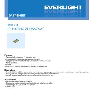
This document provides the complete technical specifications for a surface-mount device (SMD) LED identified as 19-118/BHC-ZL1M2QY/3T. This is a mono-color, blue LED designed for high-density electronic assemblies.
1.1 Core Advantages and Product Positioning
The primary advantage of this component is its compact SMD package, which enables significant reductions in board size and equipment footprint compared to traditional lead-frame type LEDs. This miniaturization supports higher packing density on PCBs and reduces storage space requirements. The lightweight nature of the package makes it particularly suitable for miniature and space-constrained applications. The product is compliant with Pb-free manufacturing processes and is designed to remain within RoHS compliance standards.
1.2 Target Applications
This LED is versatile and finds use in several key application areas:
- Backlighting: Ideal for dashboard indicators and switch illumination.
- Telecommunications: Serves as status indicators and backlighting for devices such as telephones and fax machines.
- Display Technology: Used for flat backlighting of LCDs, switches, and symbols.
- General Purpose: Suitable for a wide range of indicator and illumination tasks in consumer and industrial electronics.
2. Technical Parameter Deep-Dive
This section provides a detailed, objective analysis of the LED's key performance parameters under standard test conditions (Ta=25°C).
2.1 Device Selection and Material Composition
The LED chip is constructed using Indium Gallium Nitride (InGaN) semiconductor material, which is responsible for emitting blue light. The encapsulating resin is water-clear, optimizing light output and color purity.
2.2 Absolute Maximum Ratings
These ratings define the limits beyond which permanent damage to the device may occur. Operation under or at these conditions is not guaranteed.
- Reverse Voltage (VR): 5 V - Exceeding this voltage in reverse bias can damage the LED junction.
- Continuous Forward Current (IF): 25 mA - The maximum DC current for reliable operation.
- Peak Forward Current (IFP): 100 mA (Duty 1/10 @1KHz) - Suitable for pulsed operation but not for continuous use.
- Power Dissipation (Pd): 95 mW - The maximum power the package can dissipate as heat.
- Electrostatic Discharge (ESD) Human Body Model (HBM): 2000 V - Indicates a moderate level of ESD sensitivity; proper handling procedures are necessary.
- Operating Temperature (Topr): -40°C to +85°C - The ambient temperature range for normal operation.
- Storage Temperature (Tstg): -40°C to +90°C.
- Soldering Temperature: The device can withstand reflow soldering at 260°C for 10 seconds or hand soldering at 350°C for 3 seconds.
2.3 Electro-Optical Characteristics
These parameters define the light output and electrical behavior under a standard test current of 5mA.
- Luminous Intensity (Iv): Ranges from a minimum of 11.5 mcd to a maximum of 28.5 mcd. The typical value is not specified, indicating performance is managed through a binning system.
- Viewing Angle (2θ1/2): 120 degrees (typical). This wide viewing angle makes it suitable for applications requiring broad illumination or visibility from multiple angles.
- Peak Wavelength (λp): 468 nm (typical). This is the wavelength at which the spectral power distribution is maximum.
- Dominant Wavelength (λd): Ranges from 465 nm to 475 nm. This is the single wavelength perceived by the human eye, closely related to the color point.
- Spectral Bandwidth (Δλ): 35 nm (typical). This defines the spread of the emitted spectrum around the peak wavelength.
- Forward Voltage (VF): Ranges from 2.7 V to 3.2 V at 5mA. Designers must account for this voltage range when selecting current-limiting resistors.
Note on Tolerances: The datasheet specifies manufacturing tolerances: Luminous Intensity (±11%), Dominant Wavelength (±1nm), and Forward Voltage (±0.05V). These are critical for understanding the variance between individual units.
3. Binning System Explanation
To ensure consistency in applications, LEDs are sorted (binned) based on key parameters. This device uses a three-dimensional binning system.
3.1 Luminous Intensity Binning
LEDs are categorized into four bins (L1, L2, M1, M2) based on their measured luminous intensity at IF=5mA. This allows designers to select the brightness grade required for their application, ensuring uniform appearance in multi-LED designs.
3.2 Dominant Wavelength Binning
The color (hue) is controlled by sorting into two wavelength bins: X (465-470 nm) and Y (470-475 nm). This minimizes color variation within an assembly.
3.3 Forward Voltage Binning
LEDs are binned into five groups (29 to 33) based on their forward voltage drop at IF=5mA. Knowing the VF bin can help in designing more consistent current drive circuits, especially when LEDs are connected in parallel.
4. Performance Curve Analysis
The datasheet includes several characteristic curves that illustrate device behavior under varying conditions. These are essential for robust circuit design.
- Relative Luminous Intensity vs. Forward Current: Shows how light output increases with current. It is non-linear, and operating above the recommended current leads to diminishing returns and increased heat.
- Forward Voltage vs. Forward Current: Demonstrates the diode's IV characteristic. The voltage increases logarithmically with current.
- Forward Current Derating Curve: Indicates how the maximum allowable continuous forward current must be reduced as the ambient temperature increases above 25°C to prevent overheating.
- Luminous Intensity vs. Ambient Temperature: Shows that light output typically decreases as the junction temperature rises, a key consideration for thermal management.
- Spectrum Distribution: A graph of relative intensity versus wavelength, centered around 468 nm with a typical 35 nm bandwidth.
- Radiation Diagram: A polar plot illustrating the spatial distribution of light intensity, confirming the 120-degree viewing angle.
5. Mechanical and Package Information
5.1 Package Dimensions
The datasheet provides a detailed dimensional drawing of the LED package. Critical dimensions include the overall length, width, and height, as well as the placement and size of the solderable terminals. All unspecified tolerances are ±0.1mm.
5.2 Recommended Solder Pad Design
A suggested solder pad layout is provided for PCB design. The datasheet explicitly states this is for reference only and should be modified based on individual manufacturing processes and thermal requirements. Proper pad design is crucial for reliable soldering and mechanical strength.
6. Soldering and Assembly Guidelines
Adherence to these guidelines is critical for maintaining device reliability and performance.
6.1 Soldering Process Compatibility
The LED is compatible with both infrared and vapor phase reflow soldering processes. A detailed Pb-free reflow soldering temperature profile is provided, specifying pre-heating, time above liquidus (217°C), peak temperature (260°C max for 10 sec max), and cooling rates. Reflow soldering should not be performed more than two times.
6.2 Hand Soldering Precautions
If hand soldering is necessary, the iron tip temperature must be below 350°C, applied for no more than 3 seconds per terminal. A low-power iron (<25W) is recommended, with an interval of more than 2 seconds between soldering each terminal to prevent thermal shock.
6.3 Storage and Moisture Sensitivity
The LEDs are packaged in moisture-resistant bags with desiccant.
- Before opening: Store at ≤30°C and ≤90% RH.
- After opening: The "floor life" is 1 year at ≤30°C and ≤60% RH. Unused parts should be resealed.
- Baking: If the desiccant indicator changes or storage time is exceeded, bake at 60±5°C for 24 hours before use in a reflow process.
6.4 Critical Application Notes
- Current Limiting: An external current-limiting resistor is mandatory. The LED's exponential IV characteristic means a small voltage change causes a large current change, which can lead to immediate failure (burn-out).
- Stress Avoidance: Do not apply mechanical stress to the LED during heating (soldering) or by warping the PCB afterward.
- Repairing: Repair after soldering is discouraged. If unavoidable, a double-head soldering iron must be used to simultaneously heat both terminals and prevent damaging thermal stress. The impact on LED characteristics must be evaluated beforehand.
7. Packaging and Ordering Information
7.1 Reel and Tape Specifications
The device is supplied in 8mm tape on 7-inch diameter reels, compatible with standard automatic pick-and-place equipment. Each reel contains 3000 pieces. Detailed dimensional drawings for the carrier tape and the reel are provided.
7.2 Label Explanation
The reel label contains several codes:
- P/N: Product Number.
- CAT: Luminous Intensity Rank (bin code).
- HUE: Chromaticity Coordinates & Dominant Wavelength Rank (bin code).
- REF: Forward Voltage Rank (bin code).
- LOT No: Traceability lot number.
8. Application Design Considerations
8.1 Circuit Design
Always use a series resistor to set the forward current. Calculate the resistor value using the maximum forward voltage from the datasheet (3.2V) and the target supply voltage to ensure the current never exceeds 25mA under worst-case conditions. Consider the forward voltage binning if designing parallel arrays to ensure current sharing.
8.2 Thermal Management
While the package is small, power dissipation (up to 95mW) generates heat. Use the derating curve to limit current at high ambient temperatures. Ensure adequate PCB copper area or thermal vias are used if operating at high currents or in warm environments to maintain junction temperature within limits and preserve luminous output and lifespan.
8.3 Optical Integration
The 120-degree viewing angle provides broad emission. For applications requiring focused light, external lenses or reflectors will be necessary. The water-clear resin is suitable for use with secondary optics.
9. Technical Comparison and Positioning
Compared to through-hole LEDs, this SMD type offers the clear advantages of miniaturization, suitability for automated assembly, and better high-frequency performance due to lower parasitic inductance. Within the SMD blue LED segment, its key differentiators are its specific combination of 468nm wavelength, wide 120-degree viewing angle, and the detailed three-parameter binning system which allows for high consistency in demanding applications. The 2000V ESD rating is standard; designs in environments with higher ESD risk may require additional external protection.
10. Frequently Asked Questions (Based on Technical Parameters)
Q: Why is a current-limiting resistor absolutely necessary?
A: The LED's forward voltage has a negative temperature coefficient and manufacturing tolerance. Without a resistor, a small increase in supply voltage or a drop in VF due to heating can cause current to rise uncontrollably, leading to rapid thermal runaway and destruction.
Q: Can I drive this LED with a 3.3V supply without a resistor?
A: No. Even if 3.3V is within the VF range (2.7-3.2V), the lack of a current limit makes the circuit extremely sensitive to variations. The current could easily exceed the 25mA maximum, damaging the LED.
Q: What do the bin codes (L1, M2, X, Y, 30, 31) mean for my design?
A> They allow you to specify the brightness, color, and electrical consistency you need. For a multi-LED display, specifying tight bins (e.g., all M1 for intensity, all X for wavelength) ensures uniform appearance. Knowing the VF bin helps predict power consumption.
Q: How many times can I reflow solder this component?
A> The datasheet specifies a maximum of two reflow soldering cycles. Each cycle subjects the component to thermal stress, and exceeding this limit can compromise internal bonds or the encapsulant.
11. Design and Usage Case Study
Scenario: Designing a status indicator panel with 20 uniform blue LEDs.
- Specification: Select bins for consistency. Choose all LEDs from intensity bin M1 (18.0-22.5 mcd) and wavelength bin X (465-470 nm) to guarantee matching brightness and color.
- Circuit Design: Using a 5V supply and a target current of 20mA (below the 25mA max for margin). Using the max VF of 3.2V, calculate R = (5V - 3.2V) / 0.020A = 90 Ohms. Use the next standard value (91 Ohms). Re-calculate actual current with min VF: I = (5V - 2.7V) / 91 = ~25.3mA (still at limit, acceptable with binning). A safer approach is to use 100 Ohms.
- PCB Layout: Place the recommended solder pads. Include a small thermal relief connecting to a ground plane to help dissipate heat, as total power for 20 LEDs could be up to ~1.3W.
- Assembly: Follow the provided reflow profile. Keep the sealed reels in a dry cabinet until ready for use in the pick-and-place machine.
12. Operational Principle
This is a semiconductor photonic device. When a forward voltage exceeding its bandgap energy is applied across the InGaN p-n junction, electrons and holes recombine. In this material system, the energy released during recombination is emitted as photons (light) with a wavelength corresponding to the bandgap energy of the InGaN alloy, which is engineered to produce blue light centered around 468 nm. The water-clear epoxy resin encapsulant protects the chip, acts as a lens to shape the light output, and enhances light extraction from the semiconductor.
13. Technology Trends
Blue InGaN LEDs represent a mature and foundational technology. Trends in the broader LED industry that influence components like this one include:
- Increased Efficiency: Ongoing development aims to improve the internal quantum efficiency (more light generated per electron) and light extraction efficiency (more light escaping the chip).
- Miniaturization: The drive for smaller devices (like this SMD LED) continues, enabling ever more compact electronic products.
- Improved Color Consistency: Advanced epitaxial growth and binning processes lead to tighter wavelength and intensity distributions, reducing the need for selective binning in some applications.
- Enhanced Reliability: Improvements in packaging materials and die attach technologies aim to increase operational lifetime and resistance to thermal and environmental stress.
This component sits within these trends, offering a reliable, standardized solution for blue indicator and backlight applications where specific wavelength and package size are key requirements.
LED Specification Terminology
Complete explanation of LED technical terms
Photoelectric Performance
| Term | Unit/Representation | Simple Explanation | Why Important |
|---|---|---|---|
| Luminous Efficacy | lm/W (lumens per watt) | Light output per watt of electricity, higher means more energy efficient. | Directly determines energy efficiency grade and electricity cost. |
| Luminous Flux | lm (lumens) | Total light emitted by source, commonly called "brightness". | Determines if the light is bright enough. |
| Viewing Angle | ° (degrees), e.g., 120° | Angle where light intensity drops to half, determines beam width. | Affects illumination range and uniformity. |
| CCT (Color Temperature) | K (Kelvin), e.g., 2700K/6500K | Warmth/coolness of light, lower values yellowish/warm, higher whitish/cool. | Determines lighting atmosphere and suitable scenarios. |
| CRI / Ra | Unitless, 0–100 | Ability to render object colors accurately, Ra≥80 is good. | Affects color authenticity, used in high-demand places like malls, museums. |
| SDCM | MacAdam ellipse steps, e.g., "5-step" | Color consistency metric, smaller steps mean more consistent color. | Ensures uniform color across same batch of LEDs. |
| Dominant Wavelength | nm (nanometers), e.g., 620nm (red) | Wavelength corresponding to color of colored LEDs. | Determines hue of red, yellow, green monochrome LEDs. |
| Spectral Distribution | Wavelength vs intensity curve | Shows intensity distribution across wavelengths. | Affects color rendering and quality. |
Electrical Parameters
| Term | Symbol | Simple Explanation | Design Considerations |
|---|---|---|---|
| Forward Voltage | Vf | Minimum voltage to turn on LED, like "starting threshold". | Driver voltage must be ≥Vf, voltages add up for series LEDs. |
| Forward Current | If | Current value for normal LED operation. | Usually constant current drive, current determines brightness & lifespan. |
| Max Pulse Current | Ifp | Peak current tolerable for short periods, used for dimming or flashing. | Pulse width & duty cycle must be strictly controlled to avoid damage. |
| Reverse Voltage | Vr | Max reverse voltage LED can withstand, beyond may cause breakdown. | Circuit must prevent reverse connection or voltage spikes. |
| Thermal Resistance | Rth (°C/W) | Resistance to heat transfer from chip to solder, lower is better. | High thermal resistance requires stronger heat dissipation. |
| ESD Immunity | V (HBM), e.g., 1000V | Ability to withstand electrostatic discharge, higher means less vulnerable. | Anti-static measures needed in production, especially for sensitive LEDs. |
Thermal Management & Reliability
| Term | Key Metric | Simple Explanation | Impact |
|---|---|---|---|
| Junction Temperature | Tj (°C) | Actual operating temperature inside LED chip. | Every 10°C reduction may double lifespan; too high causes light decay, color shift. |
| Lumen Depreciation | L70 / L80 (hours) | Time for brightness to drop to 70% or 80% of initial. | Directly defines LED "service life". |
| Lumen Maintenance | % (e.g., 70%) | Percentage of brightness retained after time. | Indicates brightness retention over long-term use. |
| Color Shift | Δu′v′ or MacAdam ellipse | Degree of color change during use. | Affects color consistency in lighting scenes. |
| Thermal Aging | Material degradation | Deterioration due to long-term high temperature. | May cause brightness drop, color change, or open-circuit failure. |
Packaging & Materials
| Term | Common Types | Simple Explanation | Features & Applications |
|---|---|---|---|
| Package Type | EMC, PPA, Ceramic | Housing material protecting chip, providing optical/thermal interface. | EMC: good heat resistance, low cost; Ceramic: better heat dissipation, longer life. |
| Chip Structure | Front, Flip Chip | Chip electrode arrangement. | Flip chip: better heat dissipation, higher efficacy, for high-power. |
| Phosphor Coating | YAG, Silicate, Nitride | Covers blue chip, converts some to yellow/red, mixes to white. | Different phosphors affect efficacy, CCT, and CRI. |
| Lens/Optics | Flat, Microlens, TIR | Optical structure on surface controlling light distribution. | Determines viewing angle and light distribution curve. |
Quality Control & Binning
| Term | Binning Content | Simple Explanation | Purpose |
|---|---|---|---|
| Luminous Flux Bin | Code e.g., 2G, 2H | Grouped by brightness, each group has min/max lumen values. | Ensures uniform brightness in same batch. |
| Voltage Bin | Code e.g., 6W, 6X | Grouped by forward voltage range. | Facilitates driver matching, improves system efficiency. |
| Color Bin | 5-step MacAdam ellipse | Grouped by color coordinates, ensuring tight range. | Guarantees color consistency, avoids uneven color within fixture. |
| CCT Bin | 2700K, 3000K etc. | Grouped by CCT, each has corresponding coordinate range. | Meets different scene CCT requirements. |
Testing & Certification
| Term | Standard/Test | Simple Explanation | Significance |
|---|---|---|---|
| LM-80 | Lumen maintenance test | Long-term lighting at constant temperature, recording brightness decay. | Used to estimate LED life (with TM-21). |
| TM-21 | Life estimation standard | Estimates life under actual conditions based on LM-80 data. | Provides scientific life prediction. |
| IESNA | Illuminating Engineering Society | Covers optical, electrical, thermal test methods. | Industry-recognized test basis. |
| RoHS / REACH | Environmental certification | Ensures no harmful substances (lead, mercury). | Market access requirement internationally. |
| ENERGY STAR / DLC | Energy efficiency certification | Energy efficiency and performance certification for lighting. | Used in government procurement, subsidy programs, enhances competitiveness. |