Table of Contents
- 1. Product Overview
- 1.1 Core Advantages and Target Market
- 1.2 Applications
- 2. Technical Parameter Deep Dive
- 2.1 Absolute Maximum Ratings
- 2.2 Electro-Optical Characteristics
- 3. Binning System Explanation
- 3.1 Luminous Intensity Binning
- 3.2 Dominant Wavelength Binning
- 4. Mechanical and Package Information
- 4.1 Package Dimensions
- 4.2 Packaging Format
- 5. Soldering and Assembly Guide
- 5.1 Storage and Moisture Sensitivity
- 5.2 Reflow Soldering Profile
- 5.3 Hand Soldering and Repair
- 6. Application Suggestions and Design Considerations
- 6.1 Current Limiting is Mandatory
- 6.2 Thermal Management
- 6.3 ESD Protection
- 7. Technical Comparison and Differentiation
- 8. Frequently Asked Questions (Based on Technical Parameters)
- 8.1 Can I drive this LED at 30 mA for higher brightness?
- 8.2 Why is the forward voltage 3.5V when other blue LEDs are around 3.0V?
- 8.3 What happens if I don't follow the moisture sensitivity instructions?
- 9. Practical Design and Usage Case
- 10. Operating Principle and Technology Trends
- 10.1 Basic Operating Principle
- 10.2 Industry Trends
- LED Specification Terminology
- Photoelectric Performance
- Electrical Parameters
- Thermal Management & Reliability
- Packaging & Materials
- Quality Control & Binning
- Testing & Certification
1. Product Overview
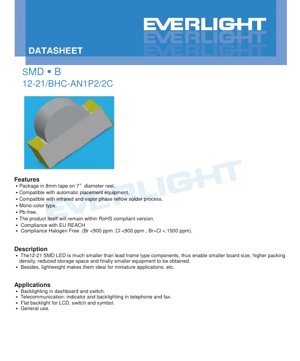
The 12-21/BHC-AN1P2/2C is a surface-mount device (SMD) light-emitting diode (LED) utilizing InGaN chip technology to produce blue light. This component is designed for modern, compact electronic assemblies, offering significant advantages in board space utilization and automated manufacturing processes.
1.1 Core Advantages and Target Market
The primary advantage of this LED is its miniature 12-21 package footprint, which is considerably smaller than traditional lead-frame type LEDs. This enables the design of smaller printed circuit boards (PCBs), higher component packing density, reduced storage requirements, and ultimately, more compact end-user equipment. Its lightweight construction makes it particularly suitable for portable and miniature applications. The product is compliant with key industry standards including RoHS, EU REACH, and is halogen-free (Br <900 ppm, Cl <900 ppm, Br+Cl < 1500 ppm), making it suitable for a wide range of consumer and industrial electronics.
1.2 Applications
Typical applications include backlighting for instrument panels, switches, and symbols; indicator and backlighting in telecommunication devices such as telephones and fax machines; flat backlighting for liquid crystal displays (LCDs); and general-purpose indicator use.
2. Technical Parameter Deep Dive
This section provides a detailed, objective interpretation of the key electrical, optical, and thermal parameters specified in the datasheet.
2.1 Absolute Maximum Ratings
These ratings define the stress limits beyond which permanent damage to the device may occur. Operation at or beyond these limits is not recommended.
- Reverse Voltage (VR): 5V. Exceeding this voltage in reverse bias can cause junction breakdown.
- Continuous Forward Current (IF): 25 mA. The maximum DC current that can be continuously applied.
- Peak Forward Current (IFP): 100 mA. This is permissible only under pulsed conditions (duty cycle 1/10 @ 1kHz) and must not be used for DC operation.
- Power Dissipation (Pd): 110 mW. The maximum power the package can dissipate, calculated as forward voltage multiplied by forward current, considering thermal limitations.
- Electrostatic Discharge (ESD) Human Body Model (HBM): 150V. This is a relatively low ESD tolerance, indicating the device is sensitive to static electricity. Proper ESD handling procedures are mandatory during assembly and handling.
- Operating & Storage Temperature: -40°C to +85°C (operating), -40°C to +90°C (storage). This wide range ensures reliability in various environmental conditions.
- Soldering Temperature: Reflow soldering is specified at 260°C peak temperature for a maximum of 10 seconds. Hand soldering should be limited to 350°C for 3 seconds per terminal.
2.2 Electro-Optical Characteristics
These parameters are measured at a standard test condition of 25°C ambient temperature and a forward current (IF) of 20 mA, unless otherwise stated.
- Luminous Intensity (Iv): Ranges from 28.5 mcd (minimum) to 72 mcd (maximum), with a typical value unspecified. The actual value is determined by the binning group (see Section 3). A ±10% tolerance is noted.
- Viewing Angle (2θ1/2): 120 degrees (typical). This wide viewing angle is characteristic of the water-clear resin dome, providing a broad emission pattern suitable for area illumination and indicators.
- Peak Wavelength (λp): 468 nm (typical). This is the wavelength at which the spectral power distribution is maximum.
- Dominant Wavelength (λd): 470 nm (typical). This is the single wavelength perceived by the human eye, defining the color. A tolerance of ±1 nm is specified.
- Spectral Bandwidth (Δλ): 35 nm (typical). This defines the width of the emitted spectrum at half the maximum intensity (FWHM).
- Forward Voltage (VF): 3.5V (typical), 4.0V (maximum) at IF=20mA. A tolerance of ±0.1V is noted. This parameter is crucial for designing the current-limiting circuitry.
- Reverse Current (IR): 50 µA (maximum) at VR=5V.
3. Binning System Explanation
The LEDs are sorted (binned) based on key optical and electrical parameters to ensure consistency within a production lot. This allows designers to select parts that meet specific application requirements.
3.1 Luminous Intensity Binning
LEDs are grouped into four intensity bins, identified by codes N1, N2, P1, and P2. The intensity range for each bin is clearly defined, with P2 representing the highest output group (57.0 - 72.0 mcd). The tolerance for luminous intensity in the binning table is noted as ±11%.
3.2 Dominant Wavelength Binning
The blue color is controlled through dominant wavelength binning. LEDs are grouped into four bins: A9 (464.5-467.5 nm), A10 (467.5-470.5 nm), A11 (470.5-473.5 nm), and A12 (473.5-476.5 nm). This ensures color consistency within a defined range. The tolerance is ±1 nm.
4. Mechanical and Package Information
4.1 Package Dimensions
The datasheet provides a detailed dimensional drawing of the 12-21 SMD package. Key dimensions include the overall length, width, and height, as well as the pad spacing and size. All unspecified tolerances are ±0.1 mm. The polarity is indicated by a marking on the package, which is essential for correct orientation during assembly.
4.2 Packaging Format
The LEDs are supplied in moisture-resistant packaging. They are housed in 8mm wide carrier tape, which is wound onto 7-inch diameter reels. Each reel contains 2000 pieces. The packaging includes a desiccant and is sealed within an aluminum moisture-proof bag to protect the components from ambient humidity during storage and transport.
5. Soldering and Assembly Guide
Proper handling is critical to ensure reliability and prevent damage to these sensitive components.
5.1 Storage and Moisture Sensitivity
This product is moisture-sensitive. The unopened bag must be stored at 30°C/90%RH or less. Once opened, the components have a "floor life" of 168 hours (7 days) under conditions of 30°C/60%RH or less. If not used within this time, or if the desiccant indicator shows saturation, the LEDs must be baked at 60 ± 5°C for 24 hours before use to remove absorbed moisture and prevent "popcorning" during reflow soldering.
5.2 Reflow Soldering Profile
A detailed Pb-free reflow soldering temperature profile is provided:
- Pre-heating: 150-200°C for 60-120 seconds.
- Time Above Liquidus (217°C): 60-150 seconds.
- Peak Temperature: 260°C maximum, held for a maximum of 10 seconds.
- Heating Rate: Maximum 6°C/second.
- Time Above 255°C: Maximum 30 seconds.
- Cooling Rate: Maximum 3°C/second.
5.3 Hand Soldering and Repair
If hand soldering is necessary, it should be performed with a soldering iron tip temperature below 350°C, applied for no more than 3 seconds per terminal. The soldering iron power should be 25W or less. A minimum interval of 2 seconds should be left between soldering each terminal. Repair after soldering is strongly discouraged. If absolutely unavoidable, a double-head soldering iron must be used to simultaneously heat both terminals, preventing thermal and mechanical stress on the LED chip.
6. Application Suggestions and Design Considerations
6.1 Current Limiting is Mandatory
The datasheet explicitly warns that an external current-limiting resistor is required. LEDs exhibit a non-linear, exponential current-voltage relationship. A small increase in forward voltage beyond the typical value can lead to a large, potentially destructive increase in current. The resistor value (R) can be calculated using Ohm's Law: R = (Supply Voltage - VF) / IF. Always use the maximum VF from the datasheet for a conservative design.
6.2 Thermal Management
While the package is small, power dissipation (up to 110 mW) generates heat. For optimal longevity and stable light output, ensure adequate thermal relief in the PCB design. This includes using appropriately sized copper pads and, if possible, thermal vias to dissipate heat to other board layers.
6.3 ESD Protection
With an ESD HBM rating of only 150V, this component is highly sensitive. Implement ESD-safe workstations, use grounded wrist straps, and transport components in conductive containers. Consider adding transient voltage suppression (TVS) diodes or other protection circuits on the PCB if the LED is connected to external interfaces prone to ESD events.
7. Technical Comparison and Differentiation
The 12-21 package offers a balance between size and ease of handling. Compared to larger SMD LEDs (e.g., 3528, 5050), it saves significant board space. Compared to smaller chip-scale packages (CSP), it is generally easier to assemble and inspect visually. Its wide 120-degree viewing angle differentiates it from narrower-beam LEDs, making it better suited for area illumination rather than focused spot lighting. The water-clear resin, as opposed to diffused resin, provides higher light output efficiency but may appear as a brighter point source.
8. Frequently Asked Questions (Based on Technical Parameters)
8.1 Can I drive this LED at 30 mA for higher brightness?
No. The Absolute Maximum Rating for continuous forward current (IF) is 25 mA. Exceeding this rating will reduce the LED's lifespan and may cause immediate failure due to overheating or electromigration within the semiconductor junction.
8.2 Why is the forward voltage 3.5V when other blue LEDs are around 3.0V?
The forward voltage is a characteristic of the semiconductor material (InGaN) and the specific epitaxial structure of the chip. A VF of 3.5V is within the typical range for blue InGaN LEDs. This must be accounted for in the power supply design.
8.3 What happens if I don't follow the moisture sensitivity instructions?
Ignoring the MSL (Moisture Sensitivity Level) instructions can lead to "popcorning" or delamination during reflow soldering. Absorbed moisture rapidly turns to steam when heated, creating internal pressure that can crack the LED resin or damage the internal wire bonds, resulting in immediate or latent failure.
9. Practical Design and Usage Case
Scenario: Designing a status indicator for a portable device. The 12-21 LED is an excellent choice due to its small size and low power consumption. The designer selects bin P1 for luminous intensity (45-57 mcd) to ensure good visibility, and bin A10 for dominant wavelength (467.5-470.5 nm) for a consistent blue color. A 3.3V system voltage is used. Calculating the series resistor: R = (3.3V - 4.0Vmax) / 0.020A. This yields a negative value, indicating 3.3V is insufficient to overcome the maximum VF. Therefore, a higher supply voltage (e.g., 5V) must be used: R = (5.0V - 4.0V) / 0.020A = 50 Ohms. A standard 51-ohm resistor is selected. The PCB layout includes ESD protection diodes on the indicator signal line and thermal relief pads connected to a ground plane.
10. Operating Principle and Technology Trends
10.1 Basic Operating Principle
This LED is based on a semiconductor p-n junction made from Indium Gallium Nitride (InGaN). When a forward voltage is applied, electrons and holes are injected into the active region where they recombine. The energy released during this recombination is emitted as photons (light). The specific composition of the InGaN alloy determines the bandgap energy and thus the wavelength (color) of the emitted light, which in this case is in the blue spectrum (~470 nm).
10.2 Industry Trends
The trend in SMD LEDs continues towards higher efficiency (more lumens per watt), smaller package sizes, and improved reliability. There is also a focus on tighter binning tolerances for color and intensity to meet the demands of applications requiring high color consistency, such as full-color displays and architectural lighting. The drive for miniaturization supports the development of even smaller packages and chip-scale packaging (CSP) technologies. Furthermore, integration of control electronics directly with the LED die (e.g., intelligent LEDs) is an ongoing area of development.
LED Specification Terminology
Complete explanation of LED technical terms
Photoelectric Performance
| Term | Unit/Representation | Simple Explanation | Why Important |
|---|---|---|---|
| Luminous Efficacy | lm/W (lumens per watt) | Light output per watt of electricity, higher means more energy efficient. | Directly determines energy efficiency grade and electricity cost. |
| Luminous Flux | lm (lumens) | Total light emitted by source, commonly called "brightness". | Determines if the light is bright enough. |
| Viewing Angle | ° (degrees), e.g., 120° | Angle where light intensity drops to half, determines beam width. | Affects illumination range and uniformity. |
| CCT (Color Temperature) | K (Kelvin), e.g., 2700K/6500K | Warmth/coolness of light, lower values yellowish/warm, higher whitish/cool. | Determines lighting atmosphere and suitable scenarios. |
| CRI / Ra | Unitless, 0–100 | Ability to render object colors accurately, Ra≥80 is good. | Affects color authenticity, used in high-demand places like malls, museums. |
| SDCM | MacAdam ellipse steps, e.g., "5-step" | Color consistency metric, smaller steps mean more consistent color. | Ensures uniform color across same batch of LEDs. |
| Dominant Wavelength | nm (nanometers), e.g., 620nm (red) | Wavelength corresponding to color of colored LEDs. | Determines hue of red, yellow, green monochrome LEDs. |
| Spectral Distribution | Wavelength vs intensity curve | Shows intensity distribution across wavelengths. | Affects color rendering and quality. |
Electrical Parameters
| Term | Symbol | Simple Explanation | Design Considerations |
|---|---|---|---|
| Forward Voltage | Vf | Minimum voltage to turn on LED, like "starting threshold". | Driver voltage must be ≥Vf, voltages add up for series LEDs. |
| Forward Current | If | Current value for normal LED operation. | Usually constant current drive, current determines brightness & lifespan. |
| Max Pulse Current | Ifp | Peak current tolerable for short periods, used for dimming or flashing. | Pulse width & duty cycle must be strictly controlled to avoid damage. |
| Reverse Voltage | Vr | Max reverse voltage LED can withstand, beyond may cause breakdown. | Circuit must prevent reverse connection or voltage spikes. |
| Thermal Resistance | Rth (°C/W) | Resistance to heat transfer from chip to solder, lower is better. | High thermal resistance requires stronger heat dissipation. |
| ESD Immunity | V (HBM), e.g., 1000V | Ability to withstand electrostatic discharge, higher means less vulnerable. | Anti-static measures needed in production, especially for sensitive LEDs. |
Thermal Management & Reliability
| Term | Key Metric | Simple Explanation | Impact |
|---|---|---|---|
| Junction Temperature | Tj (°C) | Actual operating temperature inside LED chip. | Every 10°C reduction may double lifespan; too high causes light decay, color shift. |
| Lumen Depreciation | L70 / L80 (hours) | Time for brightness to drop to 70% or 80% of initial. | Directly defines LED "service life". |
| Lumen Maintenance | % (e.g., 70%) | Percentage of brightness retained after time. | Indicates brightness retention over long-term use. |
| Color Shift | Δu′v′ or MacAdam ellipse | Degree of color change during use. | Affects color consistency in lighting scenes. |
| Thermal Aging | Material degradation | Deterioration due to long-term high temperature. | May cause brightness drop, color change, or open-circuit failure. |
Packaging & Materials
| Term | Common Types | Simple Explanation | Features & Applications |
|---|---|---|---|
| Package Type | EMC, PPA, Ceramic | Housing material protecting chip, providing optical/thermal interface. | EMC: good heat resistance, low cost; Ceramic: better heat dissipation, longer life. |
| Chip Structure | Front, Flip Chip | Chip electrode arrangement. | Flip chip: better heat dissipation, higher efficacy, for high-power. |
| Phosphor Coating | YAG, Silicate, Nitride | Covers blue chip, converts some to yellow/red, mixes to white. | Different phosphors affect efficacy, CCT, and CRI. |
| Lens/Optics | Flat, Microlens, TIR | Optical structure on surface controlling light distribution. | Determines viewing angle and light distribution curve. |
Quality Control & Binning
| Term | Binning Content | Simple Explanation | Purpose |
|---|---|---|---|
| Luminous Flux Bin | Code e.g., 2G, 2H | Grouped by brightness, each group has min/max lumen values. | Ensures uniform brightness in same batch. |
| Voltage Bin | Code e.g., 6W, 6X | Grouped by forward voltage range. | Facilitates driver matching, improves system efficiency. |
| Color Bin | 5-step MacAdam ellipse | Grouped by color coordinates, ensuring tight range. | Guarantees color consistency, avoids uneven color within fixture. |
| CCT Bin | 2700K, 3000K etc. | Grouped by CCT, each has corresponding coordinate range. | Meets different scene CCT requirements. |
Testing & Certification
| Term | Standard/Test | Simple Explanation | Significance |
|---|---|---|---|
| LM-80 | Lumen maintenance test | Long-term lighting at constant temperature, recording brightness decay. | Used to estimate LED life (with TM-21). |
| TM-21 | Life estimation standard | Estimates life under actual conditions based on LM-80 data. | Provides scientific life prediction. |
| IESNA | Illuminating Engineering Society | Covers optical, electrical, thermal test methods. | Industry-recognized test basis. |
| RoHS / REACH | Environmental certification | Ensures no harmful substances (lead, mercury). | Market access requirement internationally. |
| ENERGY STAR / DLC | Energy efficiency certification | Energy efficiency and performance certification for lighting. | Used in government procurement, subsidy programs, enhances competitiveness. |