Table of Contents
- 1. Product Overview
- 2. Technical Specifications Deep Dive
- 2.1 Absolute Maximum Ratings
- 2.2 Electro-Optical Characteristics
- 3. Binning System Explanation
- 3.1 Luminous Intensity Binning
- 3.2 Dominant Wavelength Binning
- 4. Performance Curve Analysis
- 5. Mechanical and Package Information
- 5.1 Package Dimensions
- 5.2 Reel and Tape Packaging
- 6. Soldering and Assembly Guidelines
- 6.1 Storage and Handling
- 6.2 Soldering Process
- 7. Packaging and Ordering Information
- 8. Application Recommendations
- 8.1 Typical Application Scenarios
- 8.2 Design Considerations
- 9. Technical Comparison and Differentiation
- 10. Frequently Asked Questions (FAQ)
- 11. Practical Application Example
- 12. Operating Principle
- 13. Technology Trends
- LED Specification Terminology
- Photoelectric Performance
- Electrical Parameters
- Thermal Management & Reliability
- Packaging & Materials
- Quality Control & Binning
- Testing & Certification
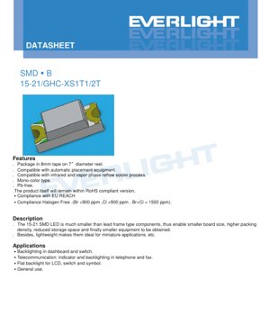
1. Product Overview
The 15-21/GHC-XS1T1/2T is a surface-mount device (SMD) LED designed for high-density, miniature applications. It features a brilliant green color emitted from an InGaN chip encapsulated in a water-clear resin package. This component is significantly smaller than traditional lead-frame LEDs, enabling more compact board designs, higher packing density, and reduced overall equipment size. Its lightweight construction makes it ideal for space-constrained and portable devices.
Key advantages include compatibility with standard automated placement equipment and reflow soldering processes (both infrared and vapor phase). The product is manufactured to be lead-free (Pb-free), compliant with the EU RoHS and REACH directives, and meets halogen-free requirements (Br <900 ppm, Cl <900 ppm, Br+Cl < 1500 ppm).
2. Technical Specifications Deep Dive
2.1 Absolute Maximum Ratings
The device must not be operated beyond these limits to prevent permanent damage. The maximum reverse voltage (VR) is 5V. The continuous forward current (IF) rating is 25 mA, with a peak forward current (IFP) of 100 mA permissible under pulsed conditions (duty cycle 1/10 @ 1kHz). The maximum power dissipation (Pd) is 95 mW. The device can withstand an electrostatic discharge (ESD) of 150V per the Human Body Model (HBM). The operating temperature range (Topr) is from -40°C to +85°C, while the storage temperature (Tstg) extends from -40°C to +90°C. Soldering temperature limits are defined for reflow (260°C max for 10 seconds) and hand soldering (350°C max for 3 seconds).
2.2 Electro-Optical Characteristics
Measured at a standard test condition of Ta=25°C and IF=20mA, the device exhibits a luminous intensity (Iv) ranging from a minimum of 180.0 mcd to a maximum of 360.0 mcd. The typical viewing angle (2θ1/2) is 130 degrees, providing a wide emission pattern. The spectral characteristics include a typical peak wavelength (λp) of 518 nm and a dominant wavelength (λd) range from 515.0 nm to 530.0 nm, defining its brilliant green color. The typical spectral bandwidth (Δλ) is 35 nm. The forward voltage (VF) typically measures 3.3V, with a range from 2.70V to 3.70V. The maximum reverse current (IR) is 50 μA when a reverse voltage (VR) of 5V is applied. Note that the device is not designed for operation under reverse bias; the VR rating is for IR testing purposes only.
3. Binning System Explanation
The LEDs are sorted into bins based on key performance parameters to ensure consistency in application design.
3.1 Luminous Intensity Binning
Under the condition IF=20mA, luminous intensity is categorized into three bins: S1 (180.0 - 225.0 mcd), S2 (225.0 - 285.0 mcd), and T1 (285.0 - 360.0 mcd). A tolerance of ±11% applies to the luminous intensity.
3.2 Dominant Wavelength Binning
Also measured at IF=20mA, the dominant wavelength is binned as follows: W (515.0 - 520.0 nm), X (520.0 - 525.0 nm), and Y (525.0 - 530.0 nm). A tolerance of ±1nm applies to the dominant wavelength.
4. Performance Curve Analysis
The datasheet includes typical electro-optical characteristic curves. These graphs visually represent the relationship between forward current and luminous intensity, the effect of ambient temperature on luminous intensity, the forward voltage versus forward current, and the spectral power distribution. Analyzing these curves is crucial for understanding device behavior under non-standard conditions, such as different drive currents or operating temperatures, which is essential for robust circuit design and thermal management.
5. Mechanical and Package Information
5.1 Package Dimensions
The LED has a compact SMD package. The dimensions are 1.6mm in length, 0.8mm in width, and 0.6mm in height, with a typical tolerance of ±0.1mm unless otherwise specified. The technical drawing provides detailed measurements for the lead positions, lens shape, and overall footprint. A cathode mark is clearly indicated on the package for correct polarity orientation during assembly.
5.2 Reel and Tape Packaging
The components are supplied in moisture-resistant packaging. They are housed in an 8mm wide carrier tape, which is wound onto a 7-inch diameter reel. Each reel contains 2000 pieces. Detailed dimensional drawings for the carrier tape pockets and the reel are provided, ensuring compatibility with automated pick-and-place machinery. The packaging includes a desiccant and is sealed within an aluminum moisture-proof bag to protect the LEDs from ambient humidity during storage and transport.
6. Soldering and Assembly Guidelines
6.1 Storage and Handling
The moisture-sensitive devices must be stored in their unopened moisture-proof bags. Once opened, the LEDs should be used within 168 hours (7 days) if kept in an environment of 30°C or less and 60% relative humidity or less. Unused LEDs should be resealed with desiccant. If the storage time is exceeded or the desiccant indicator has changed color, a baking treatment at 60 ±5°C for 24 hours is required before use.
6.2 Soldering Process
For Pb-free reflow soldering, a specific temperature profile must be followed: pre-heating between 150-200°C for 60-120 seconds, a time above liquidus (217°C) of 60-150 seconds, with a peak temperature not exceeding 260°C for a maximum of 10 seconds. The maximum ramp-up rate above 255°C is 3°C/sec, and the maximum cooling rate is 6°C/sec. Reflow soldering should not be performed more than twice. During hand soldering, the iron tip temperature must be below 350°C, applied for no more than 3 seconds per terminal, with a soldering iron power rating under 25W. A minimum interval of 2 seconds should be left between soldering each terminal. Stress on the LED body during heating and warping of the PCB after soldering must be avoided. Repair after initial soldering is not recommended, but if unavoidable, a dual-head soldering iron should be used to simultaneously heat both terminals, and the impact on device characteristics must be verified beforehand.
7. Packaging and Ordering Information
The label on the reel provides essential information for traceability and correct application: Customer's Product Number (CPN), Product Number (P/N), Packing Quantity (QTY), Luminous Intensity Rank (CAT), Chromaticity Coordinates & Dominant Wavelength Rank (HUE), Forward Voltage Rank (REF), and Lot Number (LOT No). This binning data allows designers to select components with tightly controlled parameters for their specific application needs.
8. Application Recommendations
8.1 Typical Application Scenarios
This LED is well-suited for backlighting applications in automotive dashboards and switches. In telecommunications, it serves as an indicator or backlight for phones and fax machines. It is also ideal for flat backlighting of LCDs, switches, and symbols, along with general-purpose indicator use.
8.2 Design Considerations
A current-limiting resistor is mandatory in series with the LED. The forward voltage has a range (2.7V to 3.7V), and the luminous intensity is current-dependent. Therefore, the resistor value must be calculated based on the supply voltage and the desired forward current, considering the worst-case VF to ensure the current never exceeds the absolute maximum rating of 25mA. Slight voltage shifts can cause large current changes, potentially leading to burnout. The device is not intended for high-reliability applications such as military/aerospace, automotive safety/security systems, or medical equipment without prior consultation and qualification.
9. Technical Comparison and Differentiation
Compared to larger through-hole LEDs, the primary advantage of this SMD component is its minimal footprint and height, enabling ultra-compact designs. The wide 130-degree viewing angle is beneficial for applications requiring broad illumination or visibility. The use of InGaN technology provides a saturated and brilliant green color. Its compatibility with standard Pb-free reflow profiles aligns with modern, environmentally conscious manufacturing practices. The detailed binning system offers designers a higher level of control over color and brightness consistency in their end products compared to unbinned or loosely binned alternatives.
10. Frequently Asked Questions (FAQ)
Q: What is the purpose of the binning codes (S1, T1, W, X, etc.)?
A: Binning ensures electrical and optical parameter consistency. Designers can specify a bin code to guarantee LEDs from different production lots meet the same minimum brightness (CAT code) and color (HUE code) specifications, which is critical for applications like multi-LED backlight arrays where uniformity is key.
Q: Why is storage in a moisture-proof bag so important?
A: SMD packages can absorb moisture from the air. During the high-temperature reflow soldering process, this trapped moisture can rapidly expand, causing internal delamination or "popcorning," which cracks the package and destroys the LED. The bag and baking procedures prevent this failure mode.
Q: Can I drive this LED without a series resistor?
A: No. LEDs are current-driven devices. Their forward voltage has a negative temperature coefficient and varies from unit to unit. Connecting directly to a voltage source will cause an uncontrolled and likely destructive current surge. A series resistor is the simplest form of current regulation.
Q: How do I interpret the "Peak Forward Current" rating?
A: The 100mA peak rating at a 1/10 duty cycle and 1kHz frequency allows for brief pulses of higher current, which can be used for PWM dimming to achieve an average brightness lower than the 20mA standard test current. The average current over time must still respect the 25mA continuous rating.
11. Practical Application Example
Consider designing a status indicator panel with multiple brilliant green LEDs. The designer selects the T1 brightness bin and the X wavelength bin to ensure uniform and consistent appearance. The circuit is powered by a 5V rail. Accounting for the maximum forward voltage (3.7V) and targeting a forward current of 20mA, the required series resistor value is calculated as R = (Vsupply - VF) / IF = (5V - 3.7V) / 0.020A = 65 Ohms. A standard 68 Ohm resistor would be chosen, resulting in a slightly lower current, approximately 19.1mA, which is safe and within specification. The PCB layout places the LEDs with correct polarity alignment to the cathode mark and provides adequate spacing for heat dissipation. The assembled board would then undergo a controlled reflow soldering process following the specified temperature profile.
12. Operating Principle
This LED is based on a semiconductor chip made of Indium Gallium Nitride (InGaN). When a forward voltage exceeding the diode's threshold is applied, electrons and holes are injected into the active region of the semiconductor. Their recombination releases energy in the form of photons (light). The specific composition of the InGaN alloy determines the bandgap energy, which directly corresponds to the wavelength (color) of the emitted light—in this case, brilliant green. The water-clear resin encapsulant protects the chip and acts as a lens, shaping the light output to achieve the specified 130-degree viewing angle.
13. Technology Trends
The trend in SMD LEDs continues toward higher efficiency (more light output per electrical watt), smaller package sizes for increased density, and improved color rendering and saturation. There is also a strong focus on enhancing reliability and thermal performance to support higher drive currents in compact spaces. The widespread adoption of Pb-free and halogen-free manufacturing reflects the electronics industry's commitment to environmental sustainability. Furthermore, tighter binning and more detailed characterization data provided in datasheets empower designers to create more precise and consistent optical systems for advanced applications in consumer electronics, automotive lighting, and general illumination.
LED Specification Terminology
Complete explanation of LED technical terms
Photoelectric Performance
| Term | Unit/Representation | Simple Explanation | Why Important |
|---|---|---|---|
| Luminous Efficacy | lm/W (lumens per watt) | Light output per watt of electricity, higher means more energy efficient. | Directly determines energy efficiency grade and electricity cost. |
| Luminous Flux | lm (lumens) | Total light emitted by source, commonly called "brightness". | Determines if the light is bright enough. |
| Viewing Angle | ° (degrees), e.g., 120° | Angle where light intensity drops to half, determines beam width. | Affects illumination range and uniformity. |
| CCT (Color Temperature) | K (Kelvin), e.g., 2700K/6500K | Warmth/coolness of light, lower values yellowish/warm, higher whitish/cool. | Determines lighting atmosphere and suitable scenarios. |
| CRI / Ra | Unitless, 0–100 | Ability to render object colors accurately, Ra≥80 is good. | Affects color authenticity, used in high-demand places like malls, museums. |
| SDCM | MacAdam ellipse steps, e.g., "5-step" | Color consistency metric, smaller steps mean more consistent color. | Ensures uniform color across same batch of LEDs. |
| Dominant Wavelength | nm (nanometers), e.g., 620nm (red) | Wavelength corresponding to color of colored LEDs. | Determines hue of red, yellow, green monochrome LEDs. |
| Spectral Distribution | Wavelength vs intensity curve | Shows intensity distribution across wavelengths. | Affects color rendering and quality. |
Electrical Parameters
| Term | Symbol | Simple Explanation | Design Considerations |
|---|---|---|---|
| Forward Voltage | Vf | Minimum voltage to turn on LED, like "starting threshold". | Driver voltage must be ≥Vf, voltages add up for series LEDs. |
| Forward Current | If | Current value for normal LED operation. | Usually constant current drive, current determines brightness & lifespan. |
| Max Pulse Current | Ifp | Peak current tolerable for short periods, used for dimming or flashing. | Pulse width & duty cycle must be strictly controlled to avoid damage. |
| Reverse Voltage | Vr | Max reverse voltage LED can withstand, beyond may cause breakdown. | Circuit must prevent reverse connection or voltage spikes. |
| Thermal Resistance | Rth (°C/W) | Resistance to heat transfer from chip to solder, lower is better. | High thermal resistance requires stronger heat dissipation. |
| ESD Immunity | V (HBM), e.g., 1000V | Ability to withstand electrostatic discharge, higher means less vulnerable. | Anti-static measures needed in production, especially for sensitive LEDs. |
Thermal Management & Reliability
| Term | Key Metric | Simple Explanation | Impact |
|---|---|---|---|
| Junction Temperature | Tj (°C) | Actual operating temperature inside LED chip. | Every 10°C reduction may double lifespan; too high causes light decay, color shift. |
| Lumen Depreciation | L70 / L80 (hours) | Time for brightness to drop to 70% or 80% of initial. | Directly defines LED "service life". |
| Lumen Maintenance | % (e.g., 70%) | Percentage of brightness retained after time. | Indicates brightness retention over long-term use. |
| Color Shift | Δu′v′ or MacAdam ellipse | Degree of color change during use. | Affects color consistency in lighting scenes. |
| Thermal Aging | Material degradation | Deterioration due to long-term high temperature. | May cause brightness drop, color change, or open-circuit failure. |
Packaging & Materials
| Term | Common Types | Simple Explanation | Features & Applications |
|---|---|---|---|
| Package Type | EMC, PPA, Ceramic | Housing material protecting chip, providing optical/thermal interface. | EMC: good heat resistance, low cost; Ceramic: better heat dissipation, longer life. |
| Chip Structure | Front, Flip Chip | Chip electrode arrangement. | Flip chip: better heat dissipation, higher efficacy, for high-power. |
| Phosphor Coating | YAG, Silicate, Nitride | Covers blue chip, converts some to yellow/red, mixes to white. | Different phosphors affect efficacy, CCT, and CRI. |
| Lens/Optics | Flat, Microlens, TIR | Optical structure on surface controlling light distribution. | Determines viewing angle and light distribution curve. |
Quality Control & Binning
| Term | Binning Content | Simple Explanation | Purpose |
|---|---|---|---|
| Luminous Flux Bin | Code e.g., 2G, 2H | Grouped by brightness, each group has min/max lumen values. | Ensures uniform brightness in same batch. |
| Voltage Bin | Code e.g., 6W, 6X | Grouped by forward voltage range. | Facilitates driver matching, improves system efficiency. |
| Color Bin | 5-step MacAdam ellipse | Grouped by color coordinates, ensuring tight range. | Guarantees color consistency, avoids uneven color within fixture. |
| CCT Bin | 2700K, 3000K etc. | Grouped by CCT, each has corresponding coordinate range. | Meets different scene CCT requirements. |
Testing & Certification
| Term | Standard/Test | Simple Explanation | Significance |
|---|---|---|---|
| LM-80 | Lumen maintenance test | Long-term lighting at constant temperature, recording brightness decay. | Used to estimate LED life (with TM-21). |
| TM-21 | Life estimation standard | Estimates life under actual conditions based on LM-80 data. | Provides scientific life prediction. |
| IESNA | Illuminating Engineering Society | Covers optical, electrical, thermal test methods. | Industry-recognized test basis. |
| RoHS / REACH | Environmental certification | Ensures no harmful substances (lead, mercury). | Market access requirement internationally. |
| ENERGY STAR / DLC | Energy efficiency certification | Energy efficiency and performance certification for lighting. | Used in government procurement, subsidy programs, enhances competitiveness. |