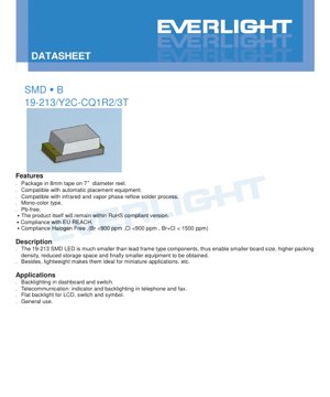
1. Product Overview
The 19-213/Y2C-CQ1 R2/3T is a surface-mount device (SMD) LED designed for high-density electronic assemblies. It is a mono-color type, emitting a brilliant yellow light, and is constructed using AlGaInP semiconductor material encapsulated in a water-clear resin. This component is significantly smaller than traditional lead-frame LEDs, enabling substantial reductions in PCB footprint, increased packing density, and ultimately contributing to the miniaturization of end equipment. Its lightweight construction makes it particularly suitable for applications where space and weight are critical constraints.
1.1 Core Features and Advantages
The primary advantages of this LED stem from its SMD package and material composition. Key features include compatibility with standard 8mm tape on 7-inch diameter reels, making it fully compatible with automated pick-and-place assembly equipment. It is designed for use with both infrared and vapor phase reflow soldering processes, aligning with modern high-volume manufacturing techniques. The device is lead-free (Pb-free) and compliant with major environmental and safety regulations including RoHS, EU REACH, and halogen-free standards (Br <900 ppm, Cl <900 ppm, Br+Cl < 1500 ppm). The product itself is maintained within RoHS compliant specifications.
1.2 Target Applications
This LED is versatile and finds use in various illumination and indication roles. Common applications include backlighting for instrument panel dashboards and switches. In telecommunications equipment, it serves as an indicator or backlight for devices such as telephones and fax machines. It is also suitable for providing flat backlighting for LCDs, switches, and symbols. Its general-purpose design makes it a reliable choice for a broad range of consumer and industrial electronic products requiring a compact, bright yellow indicator.
2. Technical Specifications and Objective Interpretation
This section provides a detailed, objective analysis of the device's operational limits and performance characteristics under standard test conditions (Ta=25°C).
2.1 Absolute Maximum Ratings
These ratings define the stress limits beyond which permanent damage to the device may occur. Operation under or at these limits is not guaranteed. The maximum reverse voltage (VR) is 5V. The continuous forward current (IF) should not exceed 25 mA. For pulsed operation, a peak forward current (IFP) of 60 mA is permissible under a duty cycle of 1/10 at 1 kHz. The maximum power dissipation (Pd) is 60 mW. The device can withstand an electrostatic discharge (ESD) of 2000V per the Human Body Model (HBM). The operational temperature range (Topr) is from -40°C to +85°C, while the storage temperature range (Tstg) is slightly wider at -40°C to +90°C. Soldering temperature limits are specified for reflow (260°C for 10 seconds max) and hand soldering (350°C for 3 seconds max at the tip).
2.2 Electro-Optical Characteristics
These parameters define the light output and electrical performance under typical operating conditions (IF=20mA, Ta=25°C). The luminous intensity (Iv) has a typical range, with specific minimum and maximum values defined by the binning system. The viewing angle (2θ1/2) is typically 120 degrees, indicating a wide radiation pattern. The peak wavelength (λp) is centered around 591 nm, and the dominant wavelength (λd) ranges from 585.5 nm to 591.5 nm, defining the perceived yellow color. The spectral bandwidth (Δλ) is approximately 15 nm. The forward voltage (VF) typically measures 2.20V, with a range from 1.70V to 2.40V. The reverse current (IR) is very low, with a maximum of 10 μA at VR=5V. It is critical to note that the device is not designed for operation under reverse bias; the VR rating applies only to the IR test condition.
3. Binning System Explanation
To ensure color and brightness consistency in production, LEDs are sorted into bins. This device uses two independent binning parameters.
3.1 Luminous Intensity Binning
The luminous output is categorized into four bins (Q1, Q2, R1, R2) when driven at 20mA. The Q1 bin covers the range from 72.0 mcd to 90.0 mcd. Q2 spans 90.0 mcd to 112.0 mcd. R1 covers 112.0 mcd to 140.0 mcd. The highest output bin, R2, ranges from 140.0 mcd to 180.0 mcd. A tolerance of ±11% applies to the luminous intensity within each bin.
3.2 Dominant Wavelength Binning
The color (dominant wavelength) is sorted into two bins (D3 and D4) to control hue variation. The D3 bin includes LEDs with a dominant wavelength between 585.5 nm and 588.5 nm. The D4 bin includes those from 588.5 nm to 591.5 nm. A tolerance of ±1 nm is specified for the dominant wavelength.
4. Performance Curve Analysis
The datasheet includes several characteristic curves that illustrate device behavior under varying conditions. These are essential for circuit design and thermal management.
4.1 Forward Current vs. Forward Voltage (I-V Curve)
This curve shows the relationship between the current flowing through the LED and the voltage drop across it. It is non-linear, typical of a diode. The curve allows designers to determine the operating voltage for a given drive current, which is crucial for selecting appropriate current-limiting resistors or designing constant-current drivers.
4.2 Relative Luminous Intensity vs. Ambient Temperature
This graph demonstrates the temperature dependence of light output. As the ambient temperature (Ta) increases, the luminous intensity typically decreases. This characteristic is vital for applications operating in elevated temperature environments, as it may necessitate optical or electrical compensation to maintain consistent brightness.
4.3 Relative Luminous Intensity vs. Forward Current
This plot shows how light output scales with drive current. While increasing current generally increases brightness, the relationship is not perfectly linear, and efficiency may drop at very high currents. It also informs the forward current derating curve, which shows the maximum allowable continuous current as a function of ambient temperature to stay within the power dissipation limits.
4.4 Spectrum Distribution and Radiation Pattern
The spectral distribution curve plots relative intensity against wavelength, confirming the peak and dominant wavelength values and showing the shape of the emitted light spectrum. The radiation diagram (polar plot) visually represents the 120-degree viewing angle, showing how light intensity is distributed spatially.
5. Mechanical and Package Information
Precise mechanical data is required for PCB layout and assembly.
5.1 Package Dimensions
The datasheet provides a detailed dimensional drawing of the LED package. All unspecified tolerances are ±0.1 mm. Designers must refer to this drawing to create the correct land pattern (footprint) on the PCB, ensuring proper soldering and alignment.
6. Soldering and Assembly Guidelines
Proper handling is critical to reliability. This device is moisture-sensitive and requires specific soldering profiles.
6.1 Storage and Moisture Sensitivity
The LEDs are packaged in a moisture-resistant bag with desiccant. The bag must not be opened until the components are ready for use. After opening, unused LEDs should be stored at ≤30°C and ≤60% relative humidity. The "floor life" after opening is 168 hours (7 days). If this time is exceeded or if the desiccant indicator shows saturation, a baking treatment at 60 ±5°C for 24 hours is required before use.
6.2 Reflow Soldering Profile
A lead-free (Pb-free) reflow profile is specified. Key parameters include a pre-heating stage between 150-200°C for 60-120 seconds, a time above liquidus (217°C) of 60-150 seconds, a peak temperature not exceeding 260°C held for a maximum of 10 seconds, and controlled ramp-up and cool-down rates (max 6°C/sec and 3°C/sec, respectively). Reflow soldering should not be performed more than twice. Stress on the LED body during heating and board warpage after soldering must be avoided.
6.3 Hand Soldering and Repair
If hand soldering is necessary, the soldering iron tip temperature must be below 350°C, applied for no more than 3 seconds per terminal. A low-power iron (<25W) is recommended, with a pause of at least 2 seconds between soldering each terminal. Repair after initial soldering is discouraged. If unavoidable, a dual-head soldering iron should be used to simultaneously heat both terminals, minimizing thermal stress. The potential for damage must be assessed beforehand.
7. Packaging and Ordering Information
The device is supplied in industry-standard packaging for automated assembly.
7.1 Reel and Tape Specifications
The LEDs are supplied on 8mm wide carrier tape wound on 7-inch diameter reels. Each reel contains 3000 pieces. Detailed dimensional drawings for the carrier tape and the reel are provided, with standard tolerances of ±0.1 mm unless otherwise noted.
7.2 Label Explanation
The packaging label contains several key identifiers: CPN (Customer's Product Number), P/N (Product Number), QTY (Packing Quantity), CAT (Luminous Intensity Rank/Bin), HUE (Chromaticity Coordinates & Dominant Wavelength Rank/Bin), REF (Forward Voltage Rank), and LOT No (Lot Number for traceability).
8. Application Design Considerations
8.1 Circuit Protection
A fundamental design rule is the mandatory use of a series current-limiting resistor. The forward voltage of an LED has a negative temperature coefficient and production variance. A slight increase in supply voltage can cause a large, potentially destructive increase in forward current if not limited by a resistor or a constant-current driver.
8.2 Thermal Management
Although a small SMD component, power dissipation (max 60 mW) and the derating of forward current with ambient temperature must be considered. Adequate PCB copper area around the thermal pads (if applicable) or general board cooling may be necessary in high-temperature or high-current applications to maintain performance and longevity.
8.3 Optical Design
The wide 120-degree viewing angle makes this LED suitable for applications requiring broad illumination or visibility from multiple angles. For focused light, secondary optics (lenses) would be required. The water-clear resin package is optimal for applications where the true chip color is desired without diffusion.
9. Frequently Asked Questions (Based on Technical Parameters)
Q: What resistor value should I use with a 5V supply?
A: Using Ohm's Law (R = (Vsupply - Vf) / If) and typical values (Vf=2.2V, If=20mA), R = (5 - 2.2) / 0.02 = 140 Ohms. A standard 150 Ohm resistor would be a safe starting point, but the minimum Vf (1.7V) should be checked to ensure current does not exceed the maximum rating.
Q: Can I drive this LED with a 3.3V microcontroller pin?
A: Yes, but efficiency will be lower. With Vf typ=2.2V and a 3.3V supply, the voltage drop across the resistor is only 1.1V. To achieve 20mA, R = 1.1 / 0.02 = 55 Ohms. Ensure the microcontroller pin can source/sink the required current.
Q: Why is the storage temperature range wider than the operating range?
A: The operating range considers active semiconductor behavior, light output, and long-term reliability under electrical stress. The storage range is for passive components where only material integrity and moisture absorption are concerns, allowing for a slightly wider temperature window.
Q: What does the "Brilliant Yellow" color refer to?
A> It describes the specific hue produced by the AlGaInP semiconductor material, corresponding to a dominant wavelength in the 585-592 nm range. It is a saturated, pure yellow compared to broader-spectrum or phosphor-converted yellows.
10. Design and Usage Case Study
Scenario: Designing a status indicator panel for a consumer appliance. A designer needs multiple bright, consistent yellow indicators on a densely populated PCB. The 19-213 LED is selected for its small size, compatibility with auto-placement, and clear binning for intensity (R1 bin chosen for high brightness) and wavelength (D4 bin for consistent color). The PCB layout uses the exact package dimensions from the datasheet. A 5V rail is available, so a 150-ohm 0805 resistor is placed in series with each LED, calculated based on typical Vf. The assembly house is instructed to follow the specified reflow profile and to bake the reels if the moisture barrier bag has been open for more than 48 hours prior to use. The wide viewing angle ensures the indicators are visible from various angles in the final product.
11. Technical Principle Introduction
This LED is based on an AlGaInP (Aluminum Gallium Indium Phosphide) semiconductor chip. When a forward voltage is applied, electrons and holes recombine in the active region of the semiconductor, releasing energy in the form of photons. The specific composition of the AlGaInP alloy determines the bandgap energy, which directly corresponds to the wavelength (color) of the emitted light—in this case, yellow (~591 nm). The chip is mounted in a surface-mount package with conductive epoxy or solder, and wire-bonded to the package leads. It is then encapsulated in a clear epoxy or silicone resin that protects the chip, acts as a lens to shape the light output, and provides mechanical stability.
12. Technology Trends and Context
SMD LEDs like the 19-213 represent the industry standard for indicator and backlight applications, having largely replaced through-hole LEDs due to manufacturing efficiency and size. The use of AlGaInP material provides high efficiency and color purity in the red, orange, and yellow spectrum. Current trends in the broader LED industry continue to focus on increasing luminous efficacy (lumens per watt), improving color rendering, further miniaturization (e.g., chip-scale packages), and enhancing reliability under higher temperature and current density. For standard indicator applications, the technology is mature, with emphasis on cost-optimized manufacturing, stringent binning for consistency, and compliance with evolving environmental regulations (halogen-free, lower carbon footprint).
LED Specification Terminology
Complete explanation of LED technical terms
Photoelectric Performance
| Term | Unit/Representation | Simple Explanation | Why Important |
|---|---|---|---|
| Luminous Efficacy | lm/W (lumens per watt) | Light output per watt of electricity, higher means more energy efficient. | Directly determines energy efficiency grade and electricity cost. |
| Luminous Flux | lm (lumens) | Total light emitted by source, commonly called "brightness". | Determines if the light is bright enough. |
| Viewing Angle | ° (degrees), e.g., 120° | Angle where light intensity drops to half, determines beam width. | Affects illumination range and uniformity. |
| CCT (Color Temperature) | K (Kelvin), e.g., 2700K/6500K | Warmth/coolness of light, lower values yellowish/warm, higher whitish/cool. | Determines lighting atmosphere and suitable scenarios. |
| CRI / Ra | Unitless, 0–100 | Ability to render object colors accurately, Ra≥80 is good. | Affects color authenticity, used in high-demand places like malls, museums. |
| SDCM | MacAdam ellipse steps, e.g., "5-step" | Color consistency metric, smaller steps mean more consistent color. | Ensures uniform color across same batch of LEDs. |
| Dominant Wavelength | nm (nanometers), e.g., 620nm (red) | Wavelength corresponding to color of colored LEDs. | Determines hue of red, yellow, green monochrome LEDs. |
| Spectral Distribution | Wavelength vs intensity curve | Shows intensity distribution across wavelengths. | Affects color rendering and quality. |
Electrical Parameters
| Term | Symbol | Simple Explanation | Design Considerations |
|---|---|---|---|
| Forward Voltage | Vf | Minimum voltage to turn on LED, like "starting threshold". | Driver voltage must be ≥Vf, voltages add up for series LEDs. |
| Forward Current | If | Current value for normal LED operation. | Usually constant current drive, current determines brightness & lifespan. |
| Max Pulse Current | Ifp | Peak current tolerable for short periods, used for dimming or flashing. | Pulse width & duty cycle must be strictly controlled to avoid damage. |
| Reverse Voltage | Vr | Max reverse voltage LED can withstand, beyond may cause breakdown. | Circuit must prevent reverse connection or voltage spikes. |
| Thermal Resistance | Rth (°C/W) | Resistance to heat transfer from chip to solder, lower is better. | High thermal resistance requires stronger heat dissipation. |
| ESD Immunity | V (HBM), e.g., 1000V | Ability to withstand electrostatic discharge, higher means less vulnerable. | Anti-static measures needed in production, especially for sensitive LEDs. |
Thermal Management & Reliability
| Term | Key Metric | Simple Explanation | Impact |
|---|---|---|---|
| Junction Temperature | Tj (°C) | Actual operating temperature inside LED chip. | Every 10°C reduction may double lifespan; too high causes light decay, color shift. |
| Lumen Depreciation | L70 / L80 (hours) | Time for brightness to drop to 70% or 80% of initial. | Directly defines LED "service life". |
| Lumen Maintenance | % (e.g., 70%) | Percentage of brightness retained after time. | Indicates brightness retention over long-term use. |
| Color Shift | Δu′v′ or MacAdam ellipse | Degree of color change during use. | Affects color consistency in lighting scenes. |
| Thermal Aging | Material degradation | Deterioration due to long-term high temperature. | May cause brightness drop, color change, or open-circuit failure. |
Packaging & Materials
| Term | Common Types | Simple Explanation | Features & Applications |
|---|---|---|---|
| Package Type | EMC, PPA, Ceramic | Housing material protecting chip, providing optical/thermal interface. | EMC: good heat resistance, low cost; Ceramic: better heat dissipation, longer life. |
| Chip Structure | Front, Flip Chip | Chip electrode arrangement. | Flip chip: better heat dissipation, higher efficacy, for high-power. |
| Phosphor Coating | YAG, Silicate, Nitride | Covers blue chip, converts some to yellow/red, mixes to white. | Different phosphors affect efficacy, CCT, and CRI. |
| Lens/Optics | Flat, Microlens, TIR | Optical structure on surface controlling light distribution. | Determines viewing angle and light distribution curve. |
Quality Control & Binning
| Term | Binning Content | Simple Explanation | Purpose |
|---|---|---|---|
| Luminous Flux Bin | Code e.g., 2G, 2H | Grouped by brightness, each group has min/max lumen values. | Ensures uniform brightness in same batch. |
| Voltage Bin | Code e.g., 6W, 6X | Grouped by forward voltage range. | Facilitates driver matching, improves system efficiency. |
| Color Bin | 5-step MacAdam ellipse | Grouped by color coordinates, ensuring tight range. | Guarantees color consistency, avoids uneven color within fixture. |
| CCT Bin | 2700K, 3000K etc. | Grouped by CCT, each has corresponding coordinate range. | Meets different scene CCT requirements. |
Testing & Certification
| Term | Standard/Test | Simple Explanation | Significance |
|---|---|---|---|
| LM-80 | Lumen maintenance test | Long-term lighting at constant temperature, recording brightness decay. | Used to estimate LED life (with TM-21). |
| TM-21 | Life estimation standard | Estimates life under actual conditions based on LM-80 data. | Provides scientific life prediction. |
| IESNA | Illuminating Engineering Society | Covers optical, electrical, thermal test methods. | Industry-recognized test basis. |
| RoHS / REACH | Environmental certification | Ensures no harmful substances (lead, mercury). | Market access requirement internationally. |
| ENERGY STAR / DLC | Energy efficiency certification | Energy efficiency and performance certification for lighting. | Used in government procurement, subsidy programs, enhances competitiveness. |