Table of Contents
- 1. Product Overview
- 1.1 Core Features and Compliance
- 1.2 Target Applications
- 2. Technical Specifications Deep Dive
- 2.1 Absolute Maximum Ratings
- 2.2 Electro-Optical Characteristics
- 3. Binning System Explanation
- 3.1 Luminous Intensity Binning
- 3.2 Dominant Wavelength Binning
- 3.3 Forward Voltage Binning
- 4. Performance Curve Analysis
- 4.1 Forward Current vs. Forward Voltage (I-V Curve)
- 4.2 Relative Luminous Intensity vs. Forward Current
- 4.3 Relative Luminous Intensity vs. Ambient Temperature
- 4.4 Forward Current Derating Curve
- 4.5 Radiation Pattern
- 4.6 Spectrum Distribution
- 5. Mechanical and Package Information
- 5.1 Package Dimensions
- 5.2 Polarity Identification
- 6. Soldering and Assembly Guidelines
- 6.1 Reflow Soldering Profile (Pb-free)
- 6.2 Hand Soldering
- 6.3 Storage and Moisture Sensitivity
- 7. Packaging and Ordering Information
- 7.1 Reel and Tape Specifications
- 7.2 Label Explanation
- 8. Application Notes and Design Considerations
- 8.1 Current Limiting is Mandatory
- 8.2 Thermal Management While the power is low (60mW max), the LED's performance and lifetime are temperature-dependent. Ensure the PCB provides adequate thermal relief, especially if multiple LEDs are used or if the ambient temperature is high. Refer to the derating curve. 8.3 ESD Precautions
- 9. Technical Comparison and Differentiation
- 10. Frequently Asked Questions (FAQs)
- 10.1 How do I select the correct current-limiting resistor?
- 10.2 Can I drive this LED without a resistor using a constant-voltage supply?
- 10.3 Why is the storage and baking process so important?
- 10.4 What does the "Y2C" in the part number signify?
- 11. Design and Usage Case Study
- 11.1 Low-Power Status Indicator Panel
- 12. Operating Principle
- 13. Technology Trends
1. Product Overview
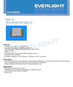
The 19-213/Y2C-CP1Q2L/3T is a surface-mount device (SMD) LED designed for high-density electronic assemblies. It is a mono-color type emitting a brilliant yellow light, utilizing AlGaInP semiconductor material encapsulated in a water-clear resin. The primary advantage of this component is its compact size, which enables significant reductions in PCB footprint, storage space, and overall equipment size compared to traditional lead-frame LEDs. Its lightweight construction further makes it ideal for miniature and portable applications.
1.1 Core Features and Compliance
- Packaged in 8mm tape on a 7-inch diameter reel for automated placement.
- Compatible with infrared and vapor phase reflow soldering processes.
- Constructed with Pb-free materials.
- Compliant with RoHS, EU REACH, and halogen-free standards (Br <900 ppm, Cl <900 ppm, Br+Cl < 1500 ppm).
1.2 Target Applications
This LED is suited for a variety of indicator and backlighting functions, including:
- Dashboard and switch backlighting in automotive and industrial controls.
- Status indicators and keypad backlighting in telecommunication devices like phones and fax machines.
- Flat backlighting for LCD panels, switches, and symbols.
- General-purpose indicator applications.
2. Technical Specifications Deep Dive
2.1 Absolute Maximum Ratings
These ratings define the limits beyond which permanent damage to the device may occur. Operation should be maintained within these boundaries.
- Reverse Voltage (VR): 5 V - Exceeding this voltage in reverse bias can cause junction breakdown.
- Continuous Forward Current (IF): 25 mA - The maximum DC current for reliable operation.
- Peak Forward Current (IFP): 60 mA (Duty 1/10 @1KHz) - For pulsed operation, short-duration peaks are permissible.
- Power Dissipation (Pd): 60 mW - The maximum power the package can dissipate, calculated as VF * IF.
- Electrostatic Discharge (ESD) HBM: 2000 V - Human Body Model rating, indicating sensitivity to static electricity.
- Operating Temperature (Topr): -40°C to +85°C - The ambient temperature range for normal operation.
- Storage Temperature (Tstg): -40°C to +90°C.
- Soldering Temperature (Tsol): Reflow: 260°C for 10 sec max; Hand: 350°C for 3 sec max per terminal.
2.2 Electro-Optical Characteristics
Measured at Ta=25°C and IF=20mA, these are the typical performance parameters.
- Luminous Intensity (Iv): 45.0 - 112.0 mcd (millicandela). The actual output is binned (see Section 3).
- Viewing Angle (2θ1/2): 120° (typical). This wide angle provides good off-axis visibility.
- Peak Wavelength (λp): 591 nm (typical). The wavelength at which the spectral emission is strongest.
- Dominant Wavelength (λd): 585.5 - 591.5 nm. This defines the perceived color (brilliant yellow) and is also binned.
- Spectral Bandwidth (Δλ): 15 nm (typical). The width of the emitted spectrum at half the peak intensity.
- Forward Voltage (VF): 1.70 - 2.30 V. The voltage drop across the LED at 20mA, which is binned.
- Reverse Current (IR): 10 μA max at VR=5V. The device is not designed for reverse operation; this parameter is for leakage test only.
Important Notes: Tolerances are specified as ±11% for luminous intensity, ±1nm for dominant wavelength, and ±0.05V for forward voltage. The reverse voltage rating applies only to the IR test condition.
3. Binning System Explanation
To ensure color and brightness consistency in production, LEDs are sorted into bins. The part number 19-213/Y2C-CP1Q2L/3T incorporates these bin codes.
3.1 Luminous Intensity Binning
Binned at IF=20mA. The code in the part number (e.g., Q2) indicates the output range.
- P1: 45.0 - 57.0 mcd
- P2: 57.0 - 72.0 mcd
- Q1: 72.0 - 90.0 mcd
- Q2: 90.0 - 112.0 mcd
3.2 Dominant Wavelength Binning
Binned at IF=20mA. Defines the color point.
- D3: 585.5 - 588.5 nm
- D4: 588.5 - 591.5 nm
3.3 Forward Voltage Binning
Binned at IF=20mA. Important for current-limiting resistor calculation and power supply design.
- 19: 1.7 - 1.8 V
- 20: 1.8 - 1.9 V
- 21: 1.9 - 2.0 V
- 22: 2.0 - 2.1 V
- 23: 2.1 - 2.2 V
- 24: 2.2 - 2.3 V
4. Performance Curve Analysis
The datasheet provides several characteristic curves essential for design.
4.1 Forward Current vs. Forward Voltage (I-V Curve)
This non-linear curve shows the relationship between current and voltage. A small increase in voltage beyond the threshold leads to a large increase in current, highlighting the necessity of a current-limiting resistor or constant-current driver.
4.2 Relative Luminous Intensity vs. Forward Current
The light output increases with current but may not be perfectly linear, especially at higher currents. Operating near the maximum rating may offer diminishing returns and increase thermal stress.
4.3 Relative Luminous Intensity vs. Ambient Temperature
LED efficiency decreases as junction temperature rises. This curve typically shows output dropping as ambient temperature increases from -40°C to +85°C. Proper thermal management on the PCB is crucial for maintaining consistent brightness.
4.4 Forward Current Derating Curve
This graph specifies the maximum allowable forward current as a function of ambient temperature. As temperature rises, the maximum safe current decreases to prevent exceeding the power dissipation limit and causing thermal runaway.
4.5 Radiation Pattern
A polar diagram showing the angular distribution of light intensity, confirming the 120° viewing angle with a typical Lambertian or side-emitter pattern.
4.6 Spectrum Distribution
A plot of relative intensity versus wavelength (approx. 550-700 nm), showing a peak around 591 nm (yellow) with a typical bandwidth of 15 nm, characteristic of AlGaInP material.
5. Mechanical and Package Information
5.1 Package Dimensions
The LED has a compact SMD package. Key dimensions (tolerance ±0.1mm unless specified) are:
- Length: 2.0 mm
- Width: 1.25 mm
- Height: 0.8 mm
- Pad dimensions and spacing are provided for PCB land pattern design.
5.2 Polarity Identification
The cathode is typically marked, often by a notch, a green dot, or a different pad size on the package underside. Correct orientation is critical for circuit operation.
6. Soldering and Assembly Guidelines
6.1 Reflow Soldering Profile (Pb-free)
A critical process for reliable assembly.
- Pre-heating: 150-200°C for 60-120 seconds.
- Time Above Liquidus (217°C): 60-150 seconds.
- Peak Temperature: 260°C maximum, held for 10 seconds maximum.
- Heating Rate: 6°C/sec maximum.
- Time Above 255°C: 30 seconds maximum.
- Cooling Rate: 3°C/sec maximum.
Important: Reflow soldering should not be performed more than two times. Avoid mechanical stress on the LED during heating and do not warp the PCB after soldering.
6.2 Hand Soldering
If manual repair is necessary:
- Use a soldering iron with a tip temperature < 350°C.
- Apply heat to each terminal for < 3 seconds.
- Use an iron with a power rating < 25W.
- Allow > 2 seconds between soldering each terminal to prevent overheating.
- Exercise extreme caution as damage is most likely during hand soldering.
6.3 Storage and Moisture Sensitivity
The components are packaged in a moisture-resistant bag.
- Do not open the moisture-proof bag until ready for use.
- After opening, unused LEDs must be stored at ≤30°C and ≤60% Relative Humidity.
- The "floor life" after opening is 168 hours (7 days).
- If the floor life is exceeded or the desiccant indicator has changed color, a bake-out is required: 60 ±5°C for 24 hours before reflow.
7. Packaging and Ordering Information
7.1 Reel and Tape Specifications
- Carrier Tape Width: 8 mm.
- Reel Diameter: 7 inches.
- Quantity per Reel: 3000 pieces.
- Detailed reel, carrier tape, and pocket dimensions are provided with ±0.1mm tolerance.
7.2 Label Explanation
The packaging label includes:
- CPN: Customer's Product Number
- P/N: Product Number (e.g., 19-213/Y2C-CP1Q2L/3T)
- QTY: Packing Quantity
- CAT: Luminous Intensity Rank (e.g., Q2)
- HUE: Chromaticity/Dominant Wavelength Rank (e.g., C, related to D3/D4)
- REF: Forward Voltage Rank (e.g., 1Q2L, related to voltage bin)
- LOT No: Traceability Lot Number
8. Application Notes and Design Considerations
8.1 Current Limiting is Mandatory
LEDs are current-driven devices. An external current-limiting resistor or constant-current driver MUST be used in series. The steep I-V curve means a small voltage change causes a large current change, which can instantly destroy the LED ("burn out"). The resistor value is calculated using Ohm's Law: R = (Vsupply - VF) / IF, where VF is the forward voltage from the appropriate bin.
8.2 Thermal Management
While the power is low (60mW max), the LED's performance and lifetime are temperature-dependent. Ensure the PCB provides adequate thermal relief, especially if multiple LEDs are used or if the ambient temperature is high. Refer to the derating curve.
8.3 ESD Precautions
With an ESD HBM rating of 2000V, this device has moderate sensitivity. Handle with ESD-safe procedures (wrist straps, grounded workstations, conductive foam) during assembly and repair.
9. Technical Comparison and Differentiation
The 19-213 LED, based on AlGaInP technology, offers distinct advantages for yellow emission:
- vs. Traditional Yellow LEDs (e.g., GaAsP): AlGaInP provides higher luminous efficiency and better color saturation (more brilliant, pure yellow), resulting in brighter output at the same current.
- vs. Phosphor-Converted White/Yellow LEDs: As a direct semiconductor emitter, it has no phosphor degradation over time, offering potentially better long-term color stability. It also has a narrower spectrum, which is desirable for specific color-filtered applications.
- vs. Larger Leaded LEDs: The SMD package enables automated assembly, higher board density, and reduced parasitic inductance, which is beneficial for high-speed switching applications.
10. Frequently Asked Questions (FAQs)
10.1 How do I select the correct current-limiting resistor?
Use the maximum forward voltage (VF) from the voltage bin specified in your order code (e.g., bin 24: 2.3V max) for a conservative design. For a 5V supply and 20mA target: R = (5V - 2.3V) / 0.020A = 135 Ohms. Use the next standard value (e.g., 150 Ohms) and calculate the resulting current: I = (5V - 2.1V_typ) / 150 = ~19.3mA, which is safe.
10.2 Can I drive this LED without a resistor using a constant-voltage supply?
No. This will almost certainly destroy the LED. The forward voltage has tolerance and varies with temperature. A constant-voltage source set to the typical VF (e.g., 2.0V) may deliver excessive current if the actual VF of the LED is lower.
10.3 Why is the storage and baking process so important?
SMD packages can absorb moisture from the air. During the high-temperature reflow soldering process, this trapped moisture can vaporize rapidly, causing internal delamination or "popcorning" that cracks the package. The moisture-resistant bag and baking procedures prevent this failure mode.
10.4 What does the "Y2C" in the part number signify?
This is a manufacturer-specific code that encapsulates the binning information for luminous intensity (CAT), dominant wavelength (HUE), and forward voltage (REF), allowing precise selection of performance characteristics.
11. Design and Usage Case Study
11.1 Low-Power Status Indicator Panel
Scenario: Designing a compact control panel with 20 yellow status indicators.
Design Choices:
- Driver Circuit: A single 5V rail is available. Using a series resistor for each LED is chosen for simplicity and cost. For bin Q2 (90-112 mcd) and voltage bin 21 (1.9-2.0V), a 150-ohm resistor is selected per LED, providing ~20mA current and bright, consistent indication.
- PCB Layout: The 2.0x1.25mm footprint allows tight spacing. A small thermal relief connection to a ground plane helps dissipate the modest 40mW per LED (2V * 20mA).
- Process: Components are ordered on 8mm tape for automated pick-and-place. The full reel is used within one shift after opening to avoid moisture sensitivity issues.
- Result: A reliable, high-density indicator array with uniform color and brightness, enabled by the small size and consistent binning of the 19-213 LED.
12. Operating Principle
The 19-213 LED is a semiconductor photonic device. It is fabricated using Aluminum Gallium Indium Phosphide (AlGaInP) epitaxial layers grown on a substrate. When a forward voltage exceeding the material's bandgap energy (approximately 1.7-2.3V) is applied, electrons and holes are injected into the active region where they recombine. This recombination process releases energy in the form of photons (light). The specific composition of the AlGaInP alloy determines the bandgap energy, which directly corresponds to the wavelength of the emitted light—in this case, brilliant yellow (~591 nm). The water-clear resin encapsulation protects the semiconductor die and acts as a lens, shaping the 120-degree radiation pattern.
13. Technology Trends
Surface-mount LEDs like the 19-213 represent the standard for modern electronic assembly due to their compatibility with automated manufacturing. Trends in this sector include:
- Increased Efficiency: Ongoing material science improvements aim to produce higher luminous efficacy (more light output per electrical watt) from AlGaInP and other compound semiconductors.
- Miniaturization: Continued reduction in package size (e.g., from 2.0mm to 1.6mm or smaller) to enable even higher density on PCBs.
- Enhanced Reliability: Improvements in packaging materials and die-attach technologies to withstand higher soldering temperatures and harsher environmental conditions.
- Tighter Binning: Advanced sorting and testing allow for narrower performance bins, giving designers more precise control over color and brightness uniformity in their products.
- Integration: A trend towards LEDs with built-in current-limiting resistors or IC drivers within the same package, simplifying circuit design.
LED Specification Terminology
Complete explanation of LED technical terms
Photoelectric Performance
| Term | Unit/Representation | Simple Explanation | Why Important |
|---|---|---|---|
| Luminous Efficacy | lm/W (lumens per watt) | Light output per watt of electricity, higher means more energy efficient. | Directly determines energy efficiency grade and electricity cost. |
| Luminous Flux | lm (lumens) | Total light emitted by source, commonly called "brightness". | Determines if the light is bright enough. |
| Viewing Angle | ° (degrees), e.g., 120° | Angle where light intensity drops to half, determines beam width. | Affects illumination range and uniformity. |
| CCT (Color Temperature) | K (Kelvin), e.g., 2700K/6500K | Warmth/coolness of light, lower values yellowish/warm, higher whitish/cool. | Determines lighting atmosphere and suitable scenarios. |
| CRI / Ra | Unitless, 0–100 | Ability to render object colors accurately, Ra≥80 is good. | Affects color authenticity, used in high-demand places like malls, museums. |
| SDCM | MacAdam ellipse steps, e.g., "5-step" | Color consistency metric, smaller steps mean more consistent color. | Ensures uniform color across same batch of LEDs. |
| Dominant Wavelength | nm (nanometers), e.g., 620nm (red) | Wavelength corresponding to color of colored LEDs. | Determines hue of red, yellow, green monochrome LEDs. |
| Spectral Distribution | Wavelength vs intensity curve | Shows intensity distribution across wavelengths. | Affects color rendering and quality. |
Electrical Parameters
| Term | Symbol | Simple Explanation | Design Considerations |
|---|---|---|---|
| Forward Voltage | Vf | Minimum voltage to turn on LED, like "starting threshold". | Driver voltage must be ≥Vf, voltages add up for series LEDs. |
| Forward Current | If | Current value for normal LED operation. | Usually constant current drive, current determines brightness & lifespan. |
| Max Pulse Current | Ifp | Peak current tolerable for short periods, used for dimming or flashing. | Pulse width & duty cycle must be strictly controlled to avoid damage. |
| Reverse Voltage | Vr | Max reverse voltage LED can withstand, beyond may cause breakdown. | Circuit must prevent reverse connection or voltage spikes. |
| Thermal Resistance | Rth (°C/W) | Resistance to heat transfer from chip to solder, lower is better. | High thermal resistance requires stronger heat dissipation. |
| ESD Immunity | V (HBM), e.g., 1000V | Ability to withstand electrostatic discharge, higher means less vulnerable. | Anti-static measures needed in production, especially for sensitive LEDs. |
Thermal Management & Reliability
| Term | Key Metric | Simple Explanation | Impact |
|---|---|---|---|
| Junction Temperature | Tj (°C) | Actual operating temperature inside LED chip. | Every 10°C reduction may double lifespan; too high causes light decay, color shift. |
| Lumen Depreciation | L70 / L80 (hours) | Time for brightness to drop to 70% or 80% of initial. | Directly defines LED "service life". |
| Lumen Maintenance | % (e.g., 70%) | Percentage of brightness retained after time. | Indicates brightness retention over long-term use. |
| Color Shift | Δu′v′ or MacAdam ellipse | Degree of color change during use. | Affects color consistency in lighting scenes. |
| Thermal Aging | Material degradation | Deterioration due to long-term high temperature. | May cause brightness drop, color change, or open-circuit failure. |
Packaging & Materials
| Term | Common Types | Simple Explanation | Features & Applications |
|---|---|---|---|
| Package Type | EMC, PPA, Ceramic | Housing material protecting chip, providing optical/thermal interface. | EMC: good heat resistance, low cost; Ceramic: better heat dissipation, longer life. |
| Chip Structure | Front, Flip Chip | Chip electrode arrangement. | Flip chip: better heat dissipation, higher efficacy, for high-power. |
| Phosphor Coating | YAG, Silicate, Nitride | Covers blue chip, converts some to yellow/red, mixes to white. | Different phosphors affect efficacy, CCT, and CRI. |
| Lens/Optics | Flat, Microlens, TIR | Optical structure on surface controlling light distribution. | Determines viewing angle and light distribution curve. |
Quality Control & Binning
| Term | Binning Content | Simple Explanation | Purpose |
|---|---|---|---|
| Luminous Flux Bin | Code e.g., 2G, 2H | Grouped by brightness, each group has min/max lumen values. | Ensures uniform brightness in same batch. |
| Voltage Bin | Code e.g., 6W, 6X | Grouped by forward voltage range. | Facilitates driver matching, improves system efficiency. |
| Color Bin | 5-step MacAdam ellipse | Grouped by color coordinates, ensuring tight range. | Guarantees color consistency, avoids uneven color within fixture. |
| CCT Bin | 2700K, 3000K etc. | Grouped by CCT, each has corresponding coordinate range. | Meets different scene CCT requirements. |
Testing & Certification
| Term | Standard/Test | Simple Explanation | Significance |
|---|---|---|---|
| LM-80 | Lumen maintenance test | Long-term lighting at constant temperature, recording brightness decay. | Used to estimate LED life (with TM-21). |
| TM-21 | Life estimation standard | Estimates life under actual conditions based on LM-80 data. | Provides scientific life prediction. |
| IESNA | Illuminating Engineering Society | Covers optical, electrical, thermal test methods. | Industry-recognized test basis. |
| RoHS / REACH | Environmental certification | Ensures no harmful substances (lead, mercury). | Market access requirement internationally. |
| ENERGY STAR / DLC | Energy efficiency certification | Energy efficiency and performance certification for lighting. | Used in government procurement, subsidy programs, enhances competitiveness. |