Table of Contents
- 1. Product Overview
- 2. In-Depth Technical Parameter Analysis
- 2.1 Absolute Maximum Ratings
- 2.2 Electro-Optical Characteristics
- 3. Binning System Explanation
- 3.1 Luminous Intensity Bins
- 3.2 Dominant Wavelength Bins
- 3.3 Forward Voltage Bins
- 4. Performance Curve Analysis
- 5. Mechanical and Package Information
- 5.1 Package Dimensions
- 5.2 Packaging Specifications
- 6. Soldering and Assembly Guidelines
- 6.1 Reflow Soldering Profile
- 6.2 Hand Soldering and Storage
- 7. Application Notes and Design Considerations
- 7.1 Typical Applications
- 7.2 Critical Design Considerations
- 8. Application Restrictions and Reliability Notes
- 9. Technical Comparison and Differentiation
- 10. Frequently Asked Questions (FAQ)
- 11. Design and Usage Case Study
- 12. Operating Principle
- 13. Technology Trends
- LED Specification Terminology
- Photoelectric Performance
- Electrical Parameters
- Thermal Management & Reliability
- Packaging & Materials
- Quality Control & Binning
- Testing & Certification
1. Product Overview
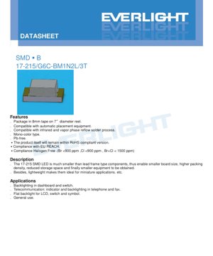
The 17-215/G6C-BM1N2L/3T is a surface-mount device (SMD) LED designed for high-density electronic assemblies. It utilizes an AIGaInP (Aluminum Gallium Indium Phosphide) semiconductor chip to produce a Brilliant Yellow Green light output. The primary advantage of this component is its miniature footprint, which enables significant reductions in printed circuit board (PCB) size, increased component packing density, and ultimately contributes to the development of smaller and lighter end-user equipment. Its lightweight construction makes it particularly suitable for applications where space and weight are critical constraints.
The LED is supplied in industry-standard 8mm tape on 7-inch diameter reels, ensuring compatibility with automated pick-and-place assembly equipment. It is engineered to be compatible with both infrared and vapor phase reflow soldering processes, facilitating modern, high-volume manufacturing. The product is classified as a mono-color type, is lead-free (Pb-free), and is confirmed to comply with major environmental and safety regulations including the EU RoHS directive, REACH regulations, and halogen-free requirements (with Bromine <900 ppm, Chlorine <900 ppm, and their sum <1500 ppm).
2. In-Depth Technical Parameter Analysis
2.1 Absolute Maximum Ratings
The absolute maximum ratings define the stress limits beyond which permanent damage to the device may occur. These values are not intended for normal operation. For the 17-215 LED, the maximum reverse voltage (VR) is 5V. Exceeding this voltage in the reverse direction can cause junction breakdown. The continuous forward current (IF) is rated at 25 mA, while a higher peak forward current (IFP) of 60 mA is permissible under pulsed conditions with a duty cycle of 1/10 at 1 kHz. The maximum power dissipation (Pd) is 60 mW, which is a critical parameter for thermal management design. The device can withstand an electrostatic discharge (ESD) of 2000V per the Human Body Model (HBM). The operating temperature range (Topr) is from -40°C to +85°C, and the storage temperature range (Tstg) is from -40°C to +90°C, indicating robust performance across a wide range of environmental conditions.
2.2 Electro-Optical Characteristics
The electro-optical characteristics are specified at a standard test condition of an ambient temperature (Ta) of 25°C and a forward current (IF) of 20 mA. The luminous intensity (Iv) ranges from a minimum of 18.0 mcd to a maximum of 45.0 mcd, with the typical value dependent on the specific bin code. The viewing angle (2θ1/2), defined as the full angle at half intensity, is typically 130 degrees, providing a wide emission pattern suitable for backlighting and indicator applications.
The spectral characteristics are defined by the peak wavelength (λp), which is typically 575 nm, and the dominant wavelength (λd), which ranges from 567.5 nm to 575.5 nm. The spectral bandwidth (Δλ) is typically 20 nm. The forward voltage (VF) required to drive the LED at 20 mA ranges from 1.7V to 2.3V, with a typical value around the midpoint of this range. The reverse current (IR) is specified at a maximum of 10 μA when a reverse voltage of 5V is applied. It is crucial to note that the device is not designed for operation under reverse bias; the VR rating is solely for testing the IR parameter.
3. Binning System Explanation
To ensure consistency in production and aid designers in selecting components for their specific needs, the LEDs are sorted into bins based on three key parameters: luminous intensity, dominant wavelength, and forward voltage.
3.1 Luminous Intensity Bins
The luminous intensity is categorized into four bins: M1 (18.0-22.5 mcd), M2 (22.5-28.5 mcd), N1 (28.5-36.0 mcd), and N2 (36.0-45.0 mcd). This allows designers to choose LEDs with the appropriate brightness level for their application, ensuring visual consistency in multi-LED arrays or meeting specific brightness requirements.
3.2 Dominant Wavelength Bins
The dominant wavelength, which correlates closely with the perceived color, is binned into four codes: C15 (567.5-569.5 nm), C16 (569.5-571.5 nm), C17 (571.5-573.5 nm), and C18 (573.5-575.5 nm). This tight binning, with a tolerance of ±1 nm, is essential for applications requiring precise color matching, such as status indicators or backlighting where color uniformity is critical.
3.3 Forward Voltage Bins
The forward voltage is divided into six bins, labeled 19 through 24, each covering a 0.1V range from 1.7V to 2.3V. Knowledge of the VF bin is important for designing efficient current-limiting circuits, especially when driving multiple LEDs in series, to ensure uniform current distribution and predictable power consumption.
4. Performance Curve Analysis
While the datasheet indicates a section for typical electro-optical characteristic curves, the specific graphs (e.g., relative luminous intensity vs. forward current, forward voltage vs. junction temperature, spectral distribution) are not provided in the extracted text. In a complete datasheet, these curves are vital for understanding device behavior under non-standard conditions. Designers typically rely on the IV curve to determine the dynamic resistance, the temperature derating curve to understand brightness reduction at high temperatures, and the spectral plot to verify color purity and full-width at half-maximum (FWHM).
5. Mechanical and Package Information
5.1 Package Dimensions
The LED features a compact SMD package. The key dimensions (in millimeters) are as follows: the overall length is 2.0 mm, the width is 1.25 mm, and the height is 0.8 mm. The cathode is typically identified by a marking or a chamfered corner on the package. The land pattern (footprint) recommendation for PCB design includes pad dimensions and spacing to ensure reliable soldering and mechanical stability. All unspecified tolerances are ±0.1 mm.
5.2 Packaging Specifications
The components are delivered in a moisture-resistant packaging system. They are housed in a carrier tape with pockets sized for the 2.0x1.25mm footprint. This carrier tape is wound onto a standard 7-inch (178 mm) diameter reel. Each reel contains 3000 pieces. The packaging includes a desiccant and is sealed within an aluminum moisture-proof bag to protect the LEDs from ambient humidity during storage and transport, which is critical for preventing "popcorning" during reflow soldering.
6. Soldering and Assembly Guidelines
6.1 Reflow Soldering Profile
For Pb-free soldering, a specific temperature profile must be followed. The pre-heating zone should ramp from 150°C to 200°C over 60-120 seconds. The time above the liquidus temperature (217°C) should be maintained for 60-150 seconds. The peak temperature must not exceed 260°C, and the time at this peak should be a maximum of 10 seconds. The maximum ramp-up rate to the peak is 6°C/sec, and the maximum time above 255°C is 30 seconds. The cooling rate should be controlled to a maximum of 3°C/sec. Reflow soldering should not be performed more than two times on the same LED.
6.2 Hand Soldering and Storage
If hand soldering is necessary, extreme care must be taken. The soldering iron tip temperature should be below 350°C, and contact time with each terminal should not exceed 3 seconds. A low-power iron (≤25W) is recommended, with an interval of at least 2 seconds between soldering each terminal. Stress should not be applied to the LED during heating, and the PCB should not be warped after soldering.
For storage, the moisture-proof bag must not be opened until the LEDs are ready for use. After opening, unused LEDs should be stored at ≤30°C and ≤60% relative humidity. The "floor life" after bag opening is 168 hours (7 days). If this time is exceeded or if the desiccant indicator shows saturation, a baking treatment at 60±5°C for 24 hours is required before use.
7. Application Notes and Design Considerations
7.1 Typical Applications
This LED is well-suited for a variety of indicator and backlighting functions. Common applications include backlighting for automotive dashboards and switches, status indicators and keypad backlighting in telecommunication devices (telephones, fax machines), flat backlighting for small LCD panels, and general-purpose indicator use where a bright yellow-green signal is required.
7.2 Critical Design Considerations
Current Limiting: An external current-limiting resistor is mandatory. LEDs exhibit a highly non-linear IV characteristic; a small increase in forward voltage beyond the nominal value can cause a large, potentially destructive increase in current. The resistor value must be calculated based on the supply voltage, the forward voltage of the LED (considering its bin), and the desired operating current (≤25 mA continuous).
Thermal Management: Although the power dissipation is low (60 mW max), proper thermal design on the PCB is still important, especially when operating at high ambient temperatures or in enclosed spaces. Adequate copper area around the thermal pads can help dissipate heat and maintain LED performance and longevity.
ESD Protection: While the LED has a 2000V HBM ESD rating, standard ESD handling precautions should be observed during assembly and handling to prevent latent damage.
8. Application Restrictions and Reliability Notes
This product is designed for general commercial and industrial applications. It is explicitly stated that it may not be suitable for high-reliability applications without prior consultation. These restricted applications include military and aerospace systems, automotive safety and security systems (e.g., airbag controls, brake lights), and life-critical medical equipment. For such uses, products with different specifications, qualification levels, and reliability data are typically required. The performance guarantees provided in this datasheet apply only when the device is operated within the specified absolute maximum ratings and recommended operating conditions.
9. Technical Comparison and Differentiation
The primary differentiator of this LED is its combination of a specific AIGaInP chip material yielding a Brilliant Yellow Green color with a very compact 2.0x1.25mm SMD package. Compared to older through-hole or larger SMD LEDs, it offers significant space savings. The wide 130-degree viewing angle is advantageous for applications requiring broad illumination rather than a focused beam. Its compliance with modern environmental standards (RoHS, REACH, Halogen-Free) makes it suitable for products with strict material declarations. The detailed binning system provides designers with a high level of control over color and brightness consistency in their products.
10. Frequently Asked Questions (FAQ)
Q: What is the difference between peak wavelength and dominant wavelength?
A: Peak wavelength (λp) is the wavelength at which the spectral power distribution is maximum. Dominant wavelength (λd) is the single wavelength of monochromatic light that matches the perceived color of the LED. For a narrow-band emitter like this LED, they are often close, but λd is more relevant for color specification.
Q: Can I drive this LED without a current-limiting resistor if my power supply is a constant current source?
A: Yes, a constant current driver is an excellent and often preferred method for driving LEDs, as it directly controls the primary variable (current) that determines light output and ensures stable operation regardless of forward voltage variations between units or with temperature.
Q: Why is the storage and baking procedure so important?
A: SMD packages can absorb moisture from the air. During the high-temperature reflow soldering process, this trapped moisture can vaporize rapidly, creating internal pressure that can crack the epoxy resin package (a phenomenon known as "popcorning" or "delamination"). The moisture-sensitive level (MSL) and baking procedures prevent this failure mode.
Q: How do I interpret the label on the reel?
A: The reel label contains key information: CPN (Customer's Part Number), P/N (Manufacturer's Part Number), QTY (Quantity on the reel), CAT (Luminous Intensity Bin Code), HUE (Dominant Wavelength Bin Code), REF (Forward Voltage Bin Code), and LOT No (Traceable manufacturing lot number).
11. Design and Usage Case Study
Scenario: Designing a multi-indicator panel. A designer is creating a control panel with 20 status indicators. Uniform brightness and color are critical for user experience. Using the binning information, the designer can specify LEDs from the same luminous intensity bin (e.g., all from N1) and the same dominant wavelength bin (e.g., all from C17) when placing the order. This pre-selection at the procurement stage minimizes brightness and color variation on the final assembled panel, eliminating the need for post-production calibration or sorting. Furthermore, knowing the forward voltage bin (e.g., 21 for 1.9-2.0V) allows for precise calculation of the current-limiting resistor value when connecting multiple LEDs in a series string to a 12V rail, ensuring each LED receives the intended current.
12. Operating Principle
This LED operates on the principle of electroluminescence in a semiconductor p-n junction. The active region is composed of AIGaInP (Aluminum Gallium Indium Phosphide). When a forward bias voltage is applied, electrons from the n-type region and holes from the p-type region are injected into the active region. There, they recombine, releasing energy in the form of photons. The specific bandgap energy of the AIGaInP alloy determines the wavelength of the emitted light, which in this case is in the yellow-green region of the visible spectrum (around 575 nm). The epoxy resin package serves to protect the semiconductor chip, provide mechanical stability, and acts as a primary lens to shape the light output beam.
13. Technology Trends
The general trend in SMD LED technology continues toward higher efficiency (more lumens or millicandelas per watt), smaller package sizes for increased density, and improved color consistency and rendering. There is also a strong focus on enhancing reliability and longevity under higher operating currents and temperatures. Furthermore, the drive for sustainability pushes for broader compliance with environmental regulations and the development of even more eco-friendly materials in the packaging and manufacturing processes. The detailed binning and moisture sensitivity handling procedures highlighted in this datasheet reflect the industry's move towards higher precision and reliability in automated, high-volume manufacturing environments.
LED Specification Terminology
Complete explanation of LED technical terms
Photoelectric Performance
| Term | Unit/Representation | Simple Explanation | Why Important |
|---|---|---|---|
| Luminous Efficacy | lm/W (lumens per watt) | Light output per watt of electricity, higher means more energy efficient. | Directly determines energy efficiency grade and electricity cost. |
| Luminous Flux | lm (lumens) | Total light emitted by source, commonly called "brightness". | Determines if the light is bright enough. |
| Viewing Angle | ° (degrees), e.g., 120° | Angle where light intensity drops to half, determines beam width. | Affects illumination range and uniformity. |
| CCT (Color Temperature) | K (Kelvin), e.g., 2700K/6500K | Warmth/coolness of light, lower values yellowish/warm, higher whitish/cool. | Determines lighting atmosphere and suitable scenarios. |
| CRI / Ra | Unitless, 0–100 | Ability to render object colors accurately, Ra≥80 is good. | Affects color authenticity, used in high-demand places like malls, museums. |
| SDCM | MacAdam ellipse steps, e.g., "5-step" | Color consistency metric, smaller steps mean more consistent color. | Ensures uniform color across same batch of LEDs. |
| Dominant Wavelength | nm (nanometers), e.g., 620nm (red) | Wavelength corresponding to color of colored LEDs. | Determines hue of red, yellow, green monochrome LEDs. |
| Spectral Distribution | Wavelength vs intensity curve | Shows intensity distribution across wavelengths. | Affects color rendering and quality. |
Electrical Parameters
| Term | Symbol | Simple Explanation | Design Considerations |
|---|---|---|---|
| Forward Voltage | Vf | Minimum voltage to turn on LED, like "starting threshold". | Driver voltage must be ≥Vf, voltages add up for series LEDs. |
| Forward Current | If | Current value for normal LED operation. | Usually constant current drive, current determines brightness & lifespan. |
| Max Pulse Current | Ifp | Peak current tolerable for short periods, used for dimming or flashing. | Pulse width & duty cycle must be strictly controlled to avoid damage. |
| Reverse Voltage | Vr | Max reverse voltage LED can withstand, beyond may cause breakdown. | Circuit must prevent reverse connection or voltage spikes. |
| Thermal Resistance | Rth (°C/W) | Resistance to heat transfer from chip to solder, lower is better. | High thermal resistance requires stronger heat dissipation. |
| ESD Immunity | V (HBM), e.g., 1000V | Ability to withstand electrostatic discharge, higher means less vulnerable. | Anti-static measures needed in production, especially for sensitive LEDs. |
Thermal Management & Reliability
| Term | Key Metric | Simple Explanation | Impact |
|---|---|---|---|
| Junction Temperature | Tj (°C) | Actual operating temperature inside LED chip. | Every 10°C reduction may double lifespan; too high causes light decay, color shift. |
| Lumen Depreciation | L70 / L80 (hours) | Time for brightness to drop to 70% or 80% of initial. | Directly defines LED "service life". |
| Lumen Maintenance | % (e.g., 70%) | Percentage of brightness retained after time. | Indicates brightness retention over long-term use. |
| Color Shift | Δu′v′ or MacAdam ellipse | Degree of color change during use. | Affects color consistency in lighting scenes. |
| Thermal Aging | Material degradation | Deterioration due to long-term high temperature. | May cause brightness drop, color change, or open-circuit failure. |
Packaging & Materials
| Term | Common Types | Simple Explanation | Features & Applications |
|---|---|---|---|
| Package Type | EMC, PPA, Ceramic | Housing material protecting chip, providing optical/thermal interface. | EMC: good heat resistance, low cost; Ceramic: better heat dissipation, longer life. |
| Chip Structure | Front, Flip Chip | Chip electrode arrangement. | Flip chip: better heat dissipation, higher efficacy, for high-power. |
| Phosphor Coating | YAG, Silicate, Nitride | Covers blue chip, converts some to yellow/red, mixes to white. | Different phosphors affect efficacy, CCT, and CRI. |
| Lens/Optics | Flat, Microlens, TIR | Optical structure on surface controlling light distribution. | Determines viewing angle and light distribution curve. |
Quality Control & Binning
| Term | Binning Content | Simple Explanation | Purpose |
|---|---|---|---|
| Luminous Flux Bin | Code e.g., 2G, 2H | Grouped by brightness, each group has min/max lumen values. | Ensures uniform brightness in same batch. |
| Voltage Bin | Code e.g., 6W, 6X | Grouped by forward voltage range. | Facilitates driver matching, improves system efficiency. |
| Color Bin | 5-step MacAdam ellipse | Grouped by color coordinates, ensuring tight range. | Guarantees color consistency, avoids uneven color within fixture. |
| CCT Bin | 2700K, 3000K etc. | Grouped by CCT, each has corresponding coordinate range. | Meets different scene CCT requirements. |
Testing & Certification
| Term | Standard/Test | Simple Explanation | Significance |
|---|---|---|---|
| LM-80 | Lumen maintenance test | Long-term lighting at constant temperature, recording brightness decay. | Used to estimate LED life (with TM-21). |
| TM-21 | Life estimation standard | Estimates life under actual conditions based on LM-80 data. | Provides scientific life prediction. |
| IESNA | Illuminating Engineering Society | Covers optical, electrical, thermal test methods. | Industry-recognized test basis. |
| RoHS / REACH | Environmental certification | Ensures no harmful substances (lead, mercury). | Market access requirement internationally. |
| ENERGY STAR / DLC | Energy efficiency certification | Energy efficiency and performance certification for lighting. | Used in government procurement, subsidy programs, enhances competitiveness. |