1. Product Overview
The 19-237B series is a compact, multi-color Surface Mount Device (SMD) LED designed for modern electronic applications requiring miniaturization and high reliability. This component represents a significant advancement over traditional lead-frame type LEDs, enabling substantial reductions in printed circuit board (PCB) real estate, increased component packing density, and ultimately contributing to the development of smaller and lighter end-user equipment. Its lightweight construction makes it particularly suitable for applications where space and weight are critical constraints.
1.1 Core Advantages and Product Positioning
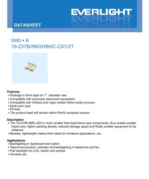
The primary advantages of the 19-237B SMD LED stem from its miniature footprint and surface-mount technology. The package is supplied on 8mm tape wound onto 7-inch diameter reels, ensuring full compatibility with automated pick-and-place assembly equipment, which is standard in high-volume manufacturing. This compatibility streamlines the production process, reduces assembly time, and minimizes potential for human error. Furthermore, the device is qualified for use with both infrared (IR) and vapor phase reflow soldering processes, offering flexibility in manufacturing line setup. A key feature is its multi-color capability within a single package footprint, provided by different semiconductor chip materials. The product is also manufactured as Pb-free and is designed to remain compliant with the Restriction of Hazardous Substances (RoHS) directive, addressing global environmental and regulatory requirements.
1.2 Target Market and Applications
The 19-237B is targeted at a broad range of consumer, industrial, and communication electronics. Its primary application domains include backlighting for instrument panel dashboards and membrane switches, providing uniform illumination. In telecommunications equipment, it serves as status indicators and keypad backlights in devices such as telephones and fax machines. It is also well-suited as a flat backlight source for liquid crystal displays (LCDs), switch panels, and symbolic icons. Finally, its general-purpose design makes it a versatile choice for various indicator and low-level illumination tasks across multiple industries.
2. Technical Parameter Deep-Dive
This section provides a detailed, objective analysis of the electrical, optical, and thermal parameters specified in the datasheet, which are critical for reliable circuit design and system integration.
2.1 Absolute Maximum Ratings
The Absolute Maximum Ratings define the stress limits beyond which permanent damage to the device may occur. These are not operating conditions. For the 19-237B series, all ratings are specified at an ambient temperature (Ta) of 25°C. The maximum reverse voltage (V_R) is 5V for all color codes. The maximum continuous forward current (I_F) is 25 mA. The peak forward current (I_FP), applicable at a duty cycle of 1/10 and 1 kHz frequency, varies: 60 mA for the R6 (Red) chip and 100 mA for both the GH (Green) and BH (Blue) chips. The maximum power dissipation (P_d) is 60 mW for R6 and 95 mW for GH/BH. The Human Body Model (HBM) electrostatic discharge (ESD) withstand voltage is 2000V for R6 and 1500V for GH/BH, indicating the red chip may have slightly more robust ESD protection. The operating temperature range (T_opr) is from -40°C to +85°C, and the storage temperature range (T_stg) is from -40°C to +90°C. The soldering temperature profile is critical: for reflow soldering, the device can withstand 260°C for 10 seconds; for hand soldering, the limit is 350°C for 3 seconds.
2.2 Electro-Optical Characteristics
The Electro-Optical Characteristics are measured at Ta=25°C and a standard test current (I_F) of 5mA, providing the key performance metrics for design.
- Luminous Intensity (I_v): This is the perceived luminous power per unit solid angle. The typical ranges are: R6: 18.0-57.0 mcd; GH: 28.5-112 mcd; BH: 11.5-28.5 mcd. The green variant typically offers the highest output.
- Viewing Angle (2θ1/2): The full angle at which the luminous intensity is half of the maximum intensity. It is typically 120 degrees, indicating a wide, diffuse emission pattern suitable for area illumination and indicators.
- Peak Wavelength (λ_p): The wavelength at which the spectral emission is maximum. Typical values are: R6: 632 nm; GH: 518 nm; BH: 468 nm.
- Dominant Wavelength (λ_d): The single wavelength perceived by the human eye that matches the color of the LED. Ranges: R6: 613-627 nm; GH: 520-535 nm; BH: 465-475 nm. Tolerances are ±1nm.
- Spectrum Radiation Bandwidth (Δλ): The spectral width at half maximum intensity. Typical: R6: 20 nm; GH: 35 nm; BH: 25 nm. A wider bandwidth, as seen in green, can affect color purity.
- Forward Voltage (V_F): The voltage drop across the LED at the test current. Ranges: R6: 1.7-2.2 V; GH: 2.6-3.3 V; BH: 2.6-3.3 V. Tolerance is ±0.10V. This parameter is crucial for current-limiting resistor calculation.
- Reverse Current (I_R): The leakage current when 5V reverse bias is applied. Max: R6: 10 μA; GH/BH: 50 μA.
3. Binning System Explanation
The datasheet defines a binning system to categorize LEDs based on key optical parameters, ensuring consistency in mass production. Designers must specify bins to guarantee color and brightness uniformity in their application.
3.1 Luminous Intensity Binning
LEDs are sorted into bins based on their measured luminous intensity at I_F=5mA.
- R6 (Red): Bins M (18.0-28.5 mcd), N (28.5-45.0 mcd), P (45.0-57.0 mcd).
- GH (Green): Bins N (28.5-45.0 mcd), P (45.0-72.0 mcd), Q (72.0-112 mcd).
- BH (Blue): Bins L (11.5-18.0 mcd), M (18.0-28.5 mcd).
The tolerance for luminous intensity is ±11% within a bin.
3.2 Dominant Wavelength Binning (for GH Green)
For the GH (Green) LED, an additional binning is provided for dominant wavelength: Bin 1 (520-525 nm), Bin 2 (525-530 nm), Bin 3 (530-535 nm). The tolerance is ±1nm. This allows for precise color selection, which is critical in applications like status indicators where color meaning is standardized.
4. Performance Curve Analysis
The datasheet includes typical characteristic curves for each LED color (R6, GH, BH), which are invaluable for understanding device behavior under non-standard conditions.
4.1 Forward Current vs. Forward Voltage (I-V Curve)
The curves show the exponential relationship between forward current and forward voltage. For all colors, the voltage increases with current. The red (R6) LED has a significantly lower forward voltage for a given current compared to the green and blue LEDs, which is characteristic of the different semiconductor materials (AlGaInP vs. InGaN). This difference must be accounted for in driver circuit design, especially in multi-color arrays.
4.2 Luminous Intensity vs. Forward Current
These plots demonstrate that luminous intensity increases approximately linearly with forward current in the typical operating range (up to ~20mA). However, efficiency (lumens per watt) may peak at a specific current and then decrease due to heating and other effects. Designers should not assume brightness scales linearly indefinitely.
4.3 Luminous Intensity vs. Ambient Temperature
This is a critical curve for thermal management. The luminous intensity for all colors decreases as the ambient temperature rises. The derating is significant, especially for the green and blue InGaN-based LEDs, which are generally more sensitive to temperature than AlGaInP red LEDs. This necessitates heat sinking or current derating in high-temperature environments to maintain brightness and longevity.
4.4 Forward Current Derating Curve
This curve specifies the maximum allowable continuous forward current as a function of ambient temperature. As temperature increases, the maximum permissible current must be reduced to prevent exceeding the device's power dissipation limit and causing thermal runaway. Adherence to this curve is essential for reliability.
4.5 Spectrum Distribution
The spectral plots show the relative intensity of light emitted across wavelengths. The red LED (R6) has a narrower, more defined peak around 632 nm. The green (GH) has a broader peak around 518 nm, and the blue (BH) has a peak around 468 nm. The shape and width of these spectra influence the color rendering and purity of the light.
4.6 Radiation Diagram
The polar radiation patterns illustrate the spatial distribution of light. The provided diagrams for each color show a typical lambertian or near-lambertian pattern, consistent with the 120-degree viewing angle. The intensity is highest at 0 degrees (perpendicular to the LED face) and decreases towards the edges.
5. Mechanical and Package Information
5.1 Package Dimensions
The 19-237B LED has a compact rectangular package. Key dimensions (in mm) are: Length: 2.0 ±0.2, Width: 1.6 ±0.2, Height: 0.9 ±0.1. The cathode is identified by a marking on the package. A detailed dimensioned drawing is provided, including lead spacing and solder pad geometry.
5.2 Suggested Pad Layout and Polarity Identification
A suggested land pattern (footprint) for PCB design is included for reference, with dimensions of 1.4mm x 0.8mm for the pads. The datasheet explicitly notes that this is a suggestion and designers should modify it based on their specific assembly process and reliability requirements. Clear polarity identification (anode mark) is shown on the package top to prevent incorrect placement.
6. Soldering and Assembly Guidelines
Proper handling and soldering are crucial for SMD components. The 19-237B is rated for standard reflow soldering profiles with a peak temperature of 260°C for a maximum of 10 seconds. For manual repair, hand soldering with an iron tip at 350°C is permissible for up to 3 seconds. It is critical to follow these guidelines to prevent damage to the LED chip or the plastic package from excessive heat. The device should be stored in its original moisture-resistant packaging until use. If exposed to ambient humidity beyond specifications, a baking process may be required before reflow to prevent \"popcorning\" (package cracking due to vapor pressure during soldering).
7. Packaging and Ordering Information
The LEDs are supplied in moisture-resistant packing on embossed carrier tape. The tape dimensions are specified. The reel has a standard 7-inch diameter. A label on the reel provides key information for traceability and verification: Customer Part Number (CPN), Manufacturer Part Number (P/N), Packing Quantity (QTY), Luminous Intensity Rank (CAT), Chromaticity/Dominant Wavelength Rank (HUE), Forward Voltage Rank (REF), and Lot Number (LOT No). This labeling system ensures correct material handling and inventory control.
8. Application Suggestions and Design Considerations
When designing with the 19-237B LED, several factors must be considered. First, always use a current-limiting resistor in series with the LED. Calculate the resistor value based on the supply voltage (V_supply), the LED's forward voltage (V_F - use max value for reliability), and the desired forward current (I_F). Formula: R = (V_supply - V_F) / I_F. Consider the power rating of the resistor. Second, account for thermal effects. If the application operates at high ambient temperatures, derate the forward current according to the provided curve to maintain longevity and stable light output. Third, for multi-color or array applications, specify tight binning codes (CAT, HUE) to ensure visual uniformity across all LEDs. Fourth, ensure the PCB pad design provides adequate solder fillet and mechanical strength. Finally, consider the viewing angle (120°) when designing light guides or lenses for the application.
9. Technical Comparison and Differentiation
Compared to larger, through-hole LEDs, the 19-237B's primary advantage is its miniature SMD footprint, enabling automated assembly and product miniaturization. Within the SMD LED landscape, its key differentiators include its specific 2.0x1.6mm package size, wide 120-degree viewing angle, and the availability of three distinct primary colors (red, green, blue) from a single package outline. The multi-wattage rating (60mW for red, 95mW for green/blue) and differing ESD ratings also distinguish it from generic offerings. Its compatibility with standard IR/vapor phase reflow and clear binning structure makes it suitable for both prototyping and high-volume, quality-conscious production.
10. Frequently Asked Questions (Based on Technical Parameters)
Q: What is the difference between peak wavelength and dominant wavelength?
A: Peak wavelength (λ_p) is the physical wavelength where the LED emits the most optical power. Dominant wavelength (λ_d) is the perceptual single wavelength that matches the color the human eye sees. They are often close but not identical, especially for LEDs with broad spectra.
Q: Why is the forward voltage different for the red LED compared to the green and blue?
A: The forward voltage is determined by the bandgap energy of the semiconductor material. Red LEDs typically use AlGaInP which has a lower bandgap (~1.8-2.0 eV) than the InGaN used for green and blue LEDs (~2.4-3.4 eV). A higher bandgap requires a higher voltage to \"push\" electrons across it.
Q: How do I interpret the binning codes (CAT, HUE, REF) on the reel label?
A: These codes correspond to the performance bins defined in the datasheet. \"CAT\" is the luminous intensity bin (e.g., N, P, Q for green). \"HUE\" is the dominant wavelength/chromaticity bin (e.g., 1, 2, 3 for green). \"REF\" is the forward voltage bin. Specifying these ensures you receive LEDs with tightly grouped characteristics.
Q: Can I drive this LED at 20mA continuously?
A: The Absolute Maximum Rating for continuous forward current (I_F) is 25 mA. Therefore, 20mA is within the specification. However, you must verify that the resulting power dissipation (P_d = V_F * I_F) does not exceed the rated 60 mW (R6) or 95 mW (GH/BH), especially at high ambient temperatures, by consulting the derating curve.
11. Practical Design Case Study
Scenario: Designing a multi-color status indicator for a consumer device. The device requires a single tri-color indicator (Red/Green/Blue) to show power, standby, and fault conditions. Using the 19-237B series, a designer would place three LEDs (R6, GH, BH) in close proximity on the PCB. To ensure color consistency, they would specify tight bins: for example, CAT=P for all to get similar high brightness, and HUE=2 for the green LED to get a specific shade. They would design three separate driver circuits, each with a current-limiting resistor calculated for the specific V_F of each color (e.g., 1.8V for red, 3.0V for green/blue from a 5V supply at 10mA). They would also ensure the PCB layout provides adequate thermal relief and follows the suggested pad dimensions to facilitate reliable soldering during automated assembly.
12. Operational Principle Introduction
Light Emitting Diodes (LEDs) are semiconductor devices that emit light through electroluminescence. When a forward voltage is applied across the p-n junction, electrons from the n-type material recombine with holes from the p-type material in the active region. This recombination releases energy in the form of photons (light particles). The color (wavelength) of the emitted light is determined by the bandgap energy of the semiconductor material used in the active region. The 19-237B uses AlGaInP for red emission and InGaN for green and blue emission. The plastic package serves to protect the fragile semiconductor chip, shape the light output (lens), and provide the electrical contacts for surface mounting.
13. Technology Trends
The SMD LED market continues to evolve towards higher efficiency (more lumens per watt), increased power density, and even smaller package sizes. There is a strong trend towards improved color rendering and consistency (tighter binning). Furthermore, the integration of control electronics, such as constant current drivers or pulse-width modulation (PWM) controllers, directly into the LED package (\"smart LEDs\") is becoming more common. Environmental regulations continue to drive the elimination of hazardous substances and improvements in recyclability. The principles embodied in the 19-237B—miniaturization, automation compatibility, and multi-color capability—remain central to these ongoing developments in solid-state lighting and indication technology.
LED Specification Terminology
Complete explanation of LED technical terms
Photoelectric Performance
| Term | Unit/Representation | Simple Explanation | Why Important |
|---|---|---|---|
| Luminous Efficacy | lm/W (lumens per watt) | Light output per watt of electricity, higher means more energy efficient. | Directly determines energy efficiency grade and electricity cost. |
| Luminous Flux | lm (lumens) | Total light emitted by source, commonly called "brightness". | Determines if the light is bright enough. |
| Viewing Angle | ° (degrees), e.g., 120° | Angle where light intensity drops to half, determines beam width. | Affects illumination range and uniformity. |
| CCT (Color Temperature) | K (Kelvin), e.g., 2700K/6500K | Warmth/coolness of light, lower values yellowish/warm, higher whitish/cool. | Determines lighting atmosphere and suitable scenarios. |
| CRI / Ra | Unitless, 0–100 | Ability to render object colors accurately, Ra≥80 is good. | Affects color authenticity, used in high-demand places like malls, museums. |
| SDCM | MacAdam ellipse steps, e.g., "5-step" | Color consistency metric, smaller steps mean more consistent color. | Ensures uniform color across same batch of LEDs. |
| Dominant Wavelength | nm (nanometers), e.g., 620nm (red) | Wavelength corresponding to color of colored LEDs. | Determines hue of red, yellow, green monochrome LEDs. |
| Spectral Distribution | Wavelength vs intensity curve | Shows intensity distribution across wavelengths. | Affects color rendering and quality. |
Electrical Parameters
| Term | Symbol | Simple Explanation | Design Considerations |
|---|---|---|---|
| Forward Voltage | Vf | Minimum voltage to turn on LED, like "starting threshold". | Driver voltage must be ≥Vf, voltages add up for series LEDs. |
| Forward Current | If | Current value for normal LED operation. | Usually constant current drive, current determines brightness & lifespan. |
| Max Pulse Current | Ifp | Peak current tolerable for short periods, used for dimming or flashing. | Pulse width & duty cycle must be strictly controlled to avoid damage. |
| Reverse Voltage | Vr | Max reverse voltage LED can withstand, beyond may cause breakdown. | Circuit must prevent reverse connection or voltage spikes. |
| Thermal Resistance | Rth (°C/W) | Resistance to heat transfer from chip to solder, lower is better. | High thermal resistance requires stronger heat dissipation. |
| ESD Immunity | V (HBM), e.g., 1000V | Ability to withstand electrostatic discharge, higher means less vulnerable. | Anti-static measures needed in production, especially for sensitive LEDs. |
Thermal Management & Reliability
| Term | Key Metric | Simple Explanation | Impact |
|---|---|---|---|
| Junction Temperature | Tj (°C) | Actual operating temperature inside LED chip. | Every 10°C reduction may double lifespan; too high causes light decay, color shift. |
| Lumen Depreciation | L70 / L80 (hours) | Time for brightness to drop to 70% or 80% of initial. | Directly defines LED "service life". |
| Lumen Maintenance | % (e.g., 70%) | Percentage of brightness retained after time. | Indicates brightness retention over long-term use. |
| Color Shift | Δu′v′ or MacAdam ellipse | Degree of color change during use. | Affects color consistency in lighting scenes. |
| Thermal Aging | Material degradation | Deterioration due to long-term high temperature. | May cause brightness drop, color change, or open-circuit failure. |
Packaging & Materials
| Term | Common Types | Simple Explanation | Features & Applications |
|---|---|---|---|
| Package Type | EMC, PPA, Ceramic | Housing material protecting chip, providing optical/thermal interface. | EMC: good heat resistance, low cost; Ceramic: better heat dissipation, longer life. |
| Chip Structure | Front, Flip Chip | Chip electrode arrangement. | Flip chip: better heat dissipation, higher efficacy, for high-power. |
| Phosphor Coating | YAG, Silicate, Nitride | Covers blue chip, converts some to yellow/red, mixes to white. | Different phosphors affect efficacy, CCT, and CRI. |
| Lens/Optics | Flat, Microlens, TIR | Optical structure on surface controlling light distribution. | Determines viewing angle and light distribution curve. |
Quality Control & Binning
| Term | Binning Content | Simple Explanation | Purpose |
|---|---|---|---|
| Luminous Flux Bin | Code e.g., 2G, 2H | Grouped by brightness, each group has min/max lumen values. | Ensures uniform brightness in same batch. |
| Voltage Bin | Code e.g., 6W, 6X | Grouped by forward voltage range. | Facilitates driver matching, improves system efficiency. |
| Color Bin | 5-step MacAdam ellipse | Grouped by color coordinates, ensuring tight range. | Guarantees color consistency, avoids uneven color within fixture. |
| CCT Bin | 2700K, 3000K etc. | Grouped by CCT, each has corresponding coordinate range. | Meets different scene CCT requirements. |
Testing & Certification
| Term | Standard/Test | Simple Explanation | Significance |
|---|---|---|---|
| LM-80 | Lumen maintenance test | Long-term lighting at constant temperature, recording brightness decay. | Used to estimate LED life (with TM-21). |
| TM-21 | Life estimation standard | Estimates life under actual conditions based on LM-80 data. | Provides scientific life prediction. |
| IESNA | Illuminating Engineering Society | Covers optical, electrical, thermal test methods. | Industry-recognized test basis. |
| RoHS / REACH | Environmental certification | Ensures no harmful substances (lead, mercury). | Market access requirement internationally. |
| ENERGY STAR / DLC | Energy efficiency certification | Energy efficiency and performance certification for lighting. | Used in government procurement, subsidy programs, enhances competitiveness. |