Table of Contents
- 1. Product Overview
- 2. Technical Parameter Deep Dive
- 2.1 Absolute Maximum Ratings
- 2.2 Electro-Optical Characteristics
- 3. Binning System Explanation
- 3.1 Luminous Intensity Binning
- 3.2 Dominant Wavelength Binning
- 3.3 Forward Voltage Binning
- 4. Performance Curve Analysis
- 5. Mechanical and Package Information
- 5.1 Package Dimension
- 5.2 Reel and Tape Packaging
- 6. Soldering and Assembly Guide
- 6.1 Storage and Handling
- 6.2 Reflow Soldering Profile
- 6.3 Hand Soldering and Repair
- 7. Packaging and Ordering Information
- 8. Application Suggestions
- 8.1 Typical Application Scenarios
- 8.2 Design Considerations
- 9. Technical Comparison and Differentiation
- 10. Frequently Asked Questions (Based on Technical Parameters)
- 11. Practical Use Case
- 12. Principle Introduction
- 13. Development Trends
- 14. Application Restrictions
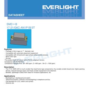
1. Product Overview
The 17-21/G6C-AN1P1B/3T is a surface-mount LED designed for high-density, miniature applications. Its compact form factor enables significant reductions in board size and equipment footprint compared to traditional lead-frame components. The device is a mono-color type, emitting a Brilliant Yellow Green light, and is constructed using AIGaInP chip technology with a water-clear resin encapsulation.
Key advantages include its compatibility with automated placement equipment and standard infrared or vapor phase reflow soldering processes. The product is fully compliant with environmental regulations, being Pb-free, RoHS compliant, EU REACH compliant, and halogen-free (Br <900 ppm, Cl <900 ppm, Br+Cl < 1500 ppm). Its lightweight nature makes it particularly suitable for space-constrained designs.
2. Technical Parameter Deep Dive
2.1 Absolute Maximum Ratings
The device's operational limits are defined under standard ambient temperature (Ta=25°C). The maximum reverse voltage (VR) is 5V. The continuous forward current (IF) rating is 25 mA, with a peak forward current (IFP) of 60 mA permissible under pulsed conditions (duty cycle 1/10 @ 1kHz). The maximum power dissipation (Pd) is 60 mW. The device can withstand an electrostatic discharge (ESD) of 2000V per the Human Body Model (HBM). The operating temperature range (Topr) is from -40°C to +85°C, while the storage temperature range (Tstg) is from -40°C to +90°C. Soldering temperature limits are specified for reflow (260°C for 10 seconds max) and hand soldering (350°C for 3 seconds max).
2.2 Electro-Optical Characteristics
Measured at Ta=25°C and a forward current of 20mA, the device exhibits a luminous intensity (Iv) ranging from 28.5 mcd to 57.0 mcd. The viewing angle (2θ1/2) is typically 140 degrees. The peak wavelength (λp) is centered around 575 nm, with a dominant wavelength (λd) range from 569.50 nm to 577.50 nm. The spectral bandwidth (Δλ) is typically 20 nm. The forward voltage (VF) ranges from 1.75V to 2.35V. The reverse current (IR) is a maximum of 10 μA when a reverse voltage of 5V is applied. Important tolerances are noted: Luminous Intensity (±11%), Dominant Wavelength (±1nm), and Forward Voltage (±0.1V). It is critical to note that the device is not designed for reverse operation; the 5V reverse rating is for IR testing only.
3. Binning System Explanation
The product is classified into bins based on key performance parameters to ensure consistency in application design.
3.1 Luminous Intensity Binning
Three bin codes are defined for luminous intensity at IF=20mA: N1 (28.5-36.0 mcd), N2 (36.0-45.0 mcd), and P1 (45.0-57.0 mcd).
3.2 Dominant Wavelength Binning
Four bin codes are defined for dominant wavelength at IF=20mA: C16 (569.50-571.50 nm), C17 (571.50-573.50 nm), C18 (573.50-575.50 nm), and C19 (575.50-577.50 nm).
3.3 Forward Voltage Binning
Three bin codes are defined for forward voltage at IF=20mA: 0 (1.75-1.95 V), 1 (1.95-2.15 V), and 2 (2.15-2.35 V).
4. Performance Curve Analysis
The datasheet references typical electro-optical characteristic curves. These curves, while not displayed in the provided text, are essential for understanding device behavior under non-standard conditions. They typically include relationships such as Luminous Intensity vs. Forward Current, Forward Voltage vs. Forward Current, and Luminous Intensity vs. Ambient Temperature. Analyzing these curves allows designers to predict performance at different drive currents and operating temperatures, which is crucial for ensuring long-term reliability and consistent light output in the final application.
5. Mechanical and Package Information
5.1 Package Dimension
The SMD package has nominal dimensions of 1.6mm in length, 0.8mm in width, and 0.6mm in height (tolerance ±0.1mm unless otherwise specified). The drawing includes a cathode mark for correct polarity identification during assembly. Precise dimensional data is critical for PCB pad design and ensuring proper solder joint formation.
5.2 Reel and Tape Packaging
The components are supplied in 8mm tape on 7-inch diameter reels, compatible with automated pick-and-place machines. Each reel contains 3000 pieces. Detailed carrier tape and reel dimensions are provided to ensure compatibility with feeder systems. The packaging is moisture-resistant, utilizing desiccant and aluminum moisture-proof bags to protect the components during storage and transit.
6. Soldering and Assembly Guide
6.1 Storage and Handling
LEDs are moisture-sensitive. The moisture-proof bag must not be opened until the products are ready for use. Before opening, store at ≤30°C and ≤90% RH. After opening, components must be used within 168 hours (7 days). Unused parts should be re-sealed in moisture-proof packaging. If the specified storage time is exceeded or the desiccant indicates moisture absorption, a baking treatment at 60±5°C for 24 hours is required before use.
6.2 Reflow Soldering Profile
A Pb-free reflow profile is specified: Preheat between 150-200°C for 60-120 seconds. The time above 217°C (liquidus) should be 60-150 seconds. The peak temperature must not exceed 260°C, and the time at or above 255°C must not exceed 30 seconds. Maximum ramp-up rate is 6°C/sec, and maximum ramp-down rate is 3°C/sec. Reflow soldering should not be performed more than two times.
6.3 Hand Soldering and Repair
For hand soldering, use a soldering iron with a tip temperature below 350°C, applied for no more than 3 seconds per terminal. The iron capacity should be less than 25W. Allow an interval of at least 2 seconds between soldering each terminal. Repair after initial soldering is discouraged. If unavoidable, a double-head soldering iron should be used to simultaneously heat both terminals and avoid mechanical stress. The potential for damage during hand soldering or repair is high.
7. Packaging and Ordering Information
The label on the reel provides key information: Customer's Product Number (CPN), Product Number (P/N), Packing Quantity (QTY), Luminous Intensity Rank (CAT), Chromaticity/Dominant Wavelength Rank (HUE), Forward Voltage Rank (REF), and Lot Number (LOT No). This binning information on the label allows designers to select and track components with specific performance characteristics for their application.
8. Application Suggestions
8.1 Typical Application Scenarios
The primary applications for this LED include backlighting for instrument panels and switches, status indicators and backlighting in telecommunication devices (phones, fax machines), flat backlighting for LCDs, switch and symbol illumination, and general-purpose indicator use.
8.2 Design Considerations
Current Limiting: An external current-limiting resistor is mandatory. The LED's exponential I-V characteristic means a small voltage change can cause a large current surge, leading to immediate failure. The resistor value must be calculated based on the supply voltage and the forward voltage bin of the LED.
Thermal Management: While the package is small, ensuring adequate PCB copper area for heat dissipation is important, especially when operating near maximum current or at high ambient temperatures, to maintain luminous output and longevity.
Placement Stress: Avoid applying mechanical stress to the component during the soldering process or when handling the assembled board.
9. Technical Comparison and Differentiation
Compared to larger through-hole LEDs, the 17-21 SMD package offers a drastic reduction in footprint and weight, enabling modern miniaturized electronics. The use of AIGaInP technology provides efficient Brilliant Yellow Green emission. Its compliance with halogen-free and other environmental standards makes it suitable for products targeting global markets with strict regulatory requirements. The defined binning structure provides a level of performance consistency important for applications requiring uniform visual appearance, such as backlighting arrays.
10. Frequently Asked Questions (Based on Technical Parameters)
Q: Can I drive this LED without a series resistor?
A: No. The datasheet explicitly warns that "slight voltage shift will cause big current change (Burn out will happen)." An external current-limiting resistor is essential for reliable operation.
Q: What is the difference between peak wavelength and dominant wavelength?
A: Peak wavelength (λp) is the wavelength at which the spectral power distribution is maximum (575 nm typ.). Dominant wavelength (λd) is the single wavelength of monochromatic light that matches the perceived color of the LED (569.5-577.5 nm). Dominant wavelength is more relevant for color specification.
Q: How many times can I reflow solder this component?
A: The datasheet states that reflow soldering should not be done more than two times. Exceeding this can damage the internal die attach or wire bonds due to repeated thermal stress.
Q: Why is there a strict 7-day limit after opening the moisture-proof bag?
A: The SMD package can absorb moisture from the atmosphere. During reflow soldering, this trapped moisture can rapidly expand, causing internal delamination or "popcorning," which cracks the package and leads to failure. The 7-day floor life is the safe exposure time for the specified moisture sensitivity level.
11. Practical Use Case
Scenario: Designing a low-power status indicator panel. A designer needs multiple uniform yellow-green indicators on a compact control board. They select the 17-21 LED for its small size. By specifying bins P1 for luminous intensity and C18 for dominant wavelength, they ensure all indicators have similar brightness and color. They design PCB pads according to the package drawing, add 100-ohm current-limiting resistors (calculated for a 5V supply and VF bin 1), and follow the reflow profile precisely. The LEDs are stored in a dry cabinet until the assembly day, used within the floor life, resulting in a reliable, visually consistent indicator panel.
12. Principle Introduction
This LED is based on an Aluminum Gallium Indium Phosphide (AIGaInP) semiconductor chip. When a forward voltage is applied, electrons and holes recombine in the active region of the semiconductor, releasing energy in the form of photons. The specific composition of the AIGaInP alloy determines the bandgap energy, which in turn defines the wavelength (color) of the emitted light—in this case, Brilliant Yellow Green. The water-clear resin encapsulation minimizes light absorption and allows for a wide viewing angle.
13. Development Trends
The trend in indicator and backlight LEDs continues toward higher efficiency (more light output per unit of electrical power), smaller package sizes for increased design density, and improved color consistency through tighter binning. There is also a strong focus on enhancing reliability under higher temperature conditions and streamlining compatibility with advanced, high-speed automated assembly processes. Environmental compliance remains a fundamental driver, pushing for materials that exceed current RoHS and halogen-free standards.
14. Application Restrictions
This product is intended for general commercial and industrial applications. It is not designed or qualified for high-reliability applications where failure could lead to personal injury, significant property damage, or substantial societal harm. This explicitly includes, but is not limited to, military/aerospace systems, automotive safety/security systems (e.g., airbag controls, braking systems), and life-supporting medical equipment. For such applications, components with different specifications, qualifications, and reliability assurances are required. The performance guarantees in this datasheet apply only when the product is used within the stated absolute maximum ratings and operating conditions.
LED Specification Terminology
Complete explanation of LED technical terms
Photoelectric Performance
| Term | Unit/Representation | Simple Explanation | Why Important |
|---|---|---|---|
| Luminous Efficacy | lm/W (lumens per watt) | Light output per watt of electricity, higher means more energy efficient. | Directly determines energy efficiency grade and electricity cost. |
| Luminous Flux | lm (lumens) | Total light emitted by source, commonly called "brightness". | Determines if the light is bright enough. |
| Viewing Angle | ° (degrees), e.g., 120° | Angle where light intensity drops to half, determines beam width. | Affects illumination range and uniformity. |
| CCT (Color Temperature) | K (Kelvin), e.g., 2700K/6500K | Warmth/coolness of light, lower values yellowish/warm, higher whitish/cool. | Determines lighting atmosphere and suitable scenarios. |
| CRI / Ra | Unitless, 0–100 | Ability to render object colors accurately, Ra≥80 is good. | Affects color authenticity, used in high-demand places like malls, museums. |
| SDCM | MacAdam ellipse steps, e.g., "5-step" | Color consistency metric, smaller steps mean more consistent color. | Ensures uniform color across same batch of LEDs. |
| Dominant Wavelength | nm (nanometers), e.g., 620nm (red) | Wavelength corresponding to color of colored LEDs. | Determines hue of red, yellow, green monochrome LEDs. |
| Spectral Distribution | Wavelength vs intensity curve | Shows intensity distribution across wavelengths. | Affects color rendering and quality. |
Electrical Parameters
| Term | Symbol | Simple Explanation | Design Considerations |
|---|---|---|---|
| Forward Voltage | Vf | Minimum voltage to turn on LED, like "starting threshold". | Driver voltage must be ≥Vf, voltages add up for series LEDs. |
| Forward Current | If | Current value for normal LED operation. | Usually constant current drive, current determines brightness & lifespan. |
| Max Pulse Current | Ifp | Peak current tolerable for short periods, used for dimming or flashing. | Pulse width & duty cycle must be strictly controlled to avoid damage. |
| Reverse Voltage | Vr | Max reverse voltage LED can withstand, beyond may cause breakdown. | Circuit must prevent reverse connection or voltage spikes. |
| Thermal Resistance | Rth (°C/W) | Resistance to heat transfer from chip to solder, lower is better. | High thermal resistance requires stronger heat dissipation. |
| ESD Immunity | V (HBM), e.g., 1000V | Ability to withstand electrostatic discharge, higher means less vulnerable. | Anti-static measures needed in production, especially for sensitive LEDs. |
Thermal Management & Reliability
| Term | Key Metric | Simple Explanation | Impact |
|---|---|---|---|
| Junction Temperature | Tj (°C) | Actual operating temperature inside LED chip. | Every 10°C reduction may double lifespan; too high causes light decay, color shift. |
| Lumen Depreciation | L70 / L80 (hours) | Time for brightness to drop to 70% or 80% of initial. | Directly defines LED "service life". |
| Lumen Maintenance | % (e.g., 70%) | Percentage of brightness retained after time. | Indicates brightness retention over long-term use. |
| Color Shift | Δu′v′ or MacAdam ellipse | Degree of color change during use. | Affects color consistency in lighting scenes. |
| Thermal Aging | Material degradation | Deterioration due to long-term high temperature. | May cause brightness drop, color change, or open-circuit failure. |
Packaging & Materials
| Term | Common Types | Simple Explanation | Features & Applications |
|---|---|---|---|
| Package Type | EMC, PPA, Ceramic | Housing material protecting chip, providing optical/thermal interface. | EMC: good heat resistance, low cost; Ceramic: better heat dissipation, longer life. |
| Chip Structure | Front, Flip Chip | Chip electrode arrangement. | Flip chip: better heat dissipation, higher efficacy, for high-power. |
| Phosphor Coating | YAG, Silicate, Nitride | Covers blue chip, converts some to yellow/red, mixes to white. | Different phosphors affect efficacy, CCT, and CRI. |
| Lens/Optics | Flat, Microlens, TIR | Optical structure on surface controlling light distribution. | Determines viewing angle and light distribution curve. |
Quality Control & Binning
| Term | Binning Content | Simple Explanation | Purpose |
|---|---|---|---|
| Luminous Flux Bin | Code e.g., 2G, 2H | Grouped by brightness, each group has min/max lumen values. | Ensures uniform brightness in same batch. |
| Voltage Bin | Code e.g., 6W, 6X | Grouped by forward voltage range. | Facilitates driver matching, improves system efficiency. |
| Color Bin | 5-step MacAdam ellipse | Grouped by color coordinates, ensuring tight range. | Guarantees color consistency, avoids uneven color within fixture. |
| CCT Bin | 2700K, 3000K etc. | Grouped by CCT, each has corresponding coordinate range. | Meets different scene CCT requirements. |
Testing & Certification
| Term | Standard/Test | Simple Explanation | Significance |
|---|---|---|---|
| LM-80 | Lumen maintenance test | Long-term lighting at constant temperature, recording brightness decay. | Used to estimate LED life (with TM-21). |
| TM-21 | Life estimation standard | Estimates life under actual conditions based on LM-80 data. | Provides scientific life prediction. |
| IESNA | Illuminating Engineering Society | Covers optical, electrical, thermal test methods. | Industry-recognized test basis. |
| RoHS / REACH | Environmental certification | Ensures no harmful substances (lead, mercury). | Market access requirement internationally. |
| ENERGY STAR / DLC | Energy efficiency certification | Energy efficiency and performance certification for lighting. | Used in government procurement, subsidy programs, enhances competitiveness. |