Table of Contents
- 1. Product Overview
- 1.1 Core Advantages and Product Positioning
- 1.2 Target Market and Applications
- 2. In-Depth Technical Parameter Analysis
- 2.1 Absolute Maximum Ratings
- 2.2 Electro-Optical Characteristics (Ta = 25°C)
- 3. Binning System Explanation
- 3.1 Luminous Intensity Binning
- 3.2 Forward Voltage Binning
- 3.3 Chromaticity Coordinate Binning
- 4. Mechanical and Package Information
- 4.1 Package Dimensions
- 4.2 Polarity Identification
- 5. Soldering and Assembly Guidelines
- 5.1 Reflow Soldering Profile
- 5.2 Hand Soldering
- 5.3 Storage and Moisture Sensitivity
- 6. Packaging and Ordering Information
- 6.1 Standard Packaging
- 6.2 Label Explanation
- 7. Application Design Considerations
- 7.1 Current Limiting is Mandatory
- 7.2 Thermal Management
- 7.3 ESD Protection
- 8. Technical Comparison and Differentiation
- 9. Frequently Asked Questions (FAQ)
- 9.1 Can I drive this LED without a current-limiting resistor?
- 9.2 What is the difference between the P1, Q2, etc., bins?
- 9.3 How many times can I reflow solder this component?
- 9.4 The bag has been open for a week. Can I still use the LEDs?
- 10. Practical Design and Usage Case
- 11. Operational Principle
- 12. Industry Trends and Context
1. Product Overview
The 12-21C/T3D-CP1Q2B12Y/2C is a compact, surface-mount LED designed for modern electronic applications requiring reliable, low-profile illumination. This component represents a significant advancement over traditional lead-frame LEDs, enabling substantial miniaturization and efficiency improvements in end-product design.
1.1 Core Advantages and Product Positioning
The primary advantage of this LED is its extremely small footprint. The package dimensions allow for higher packing density on printed circuit boards (PCBs), directly contributing to reduced board size and, consequently, smaller final equipment. Its lightweight nature makes it particularly suitable for portable and miniature applications where weight and space are critical constraints. The product is positioned as a versatile, general-purpose indicator and backlighting solution, compliant with major environmental and safety standards including RoHS, REACH, and Halogen-Free requirements (Br <900 ppm, Cl <900 ppm, Br+Cl < 1500 ppm).
1.2 Target Market and Applications
This LED is engineered for a broad range of applications across consumer electronics, automotive, and telecommunications sectors. Key application areas include backlighting for instrument clusters, switches, and symbols; indicator and backlighting functions in telecommunication devices such as telephones and fax machines; and general flat backlighting for LCD panels. Its compatibility with automatic placement equipment and standard infrared/vapor phase reflow soldering processes makes it ideal for high-volume manufacturing.
2. In-Depth Technical Parameter Analysis
A thorough understanding of the electrical and optical parameters is essential for reliable circuit design and ensuring long-term performance.
2.1 Absolute Maximum Ratings
These ratings define the stress limits beyond which permanent damage to the device may occur. They are not intended for normal operation.
- Reverse Voltage (VR): 5 V. Exceeding this voltage in reverse bias can cause immediate junction breakdown.
- Forward Current (IF): 10 mA (Continuous).
- Peak Forward Current (IFP): 100 mA (Duty Cycle 1/10 @ 1 kHz). This allows for brief pulses of higher current, useful for multiplexing or achieving higher instantaneous brightness.
- Power Dissipation (Pd): 40 mW. This is the maximum power the package can dissipate as heat without exceeding its thermal limits.
- Electrostatic Discharge (ESD): Human Body Model (HBM) 150 V. This indicates moderate sensitivity to ESD, necessitating proper handling procedures in an ESD-protected environment.
- Operating Temperature (Topr): -40°C to +85°C. This wide range suits automotive and industrial environments.
- Storage Temperature (Tstg): -40°C to +90°C.
2.2 Electro-Optical Characteristics (Ta = 25°C)
These parameters are measured under standard test conditions and define the device's performance.
- Luminous Intensity (Iv): 45.0 mcd (Min), 112.0 mcd (Max) at IF = 5 mA. The typical value is not specified, indicating performance is managed through the binning system.
- Viewing Angle (2θ1/2): 110 degrees (Typical). This wide viewing angle is characteristic of a diffused yellow resin package, providing a broad, even light distribution.
- Forward Voltage (VF): 2.70 V (Min), 3.40 V (Max) at IF = 5 mA. The tight tolerance of ±0.05V per bin ensures consistent voltage drop across production lots.
- Reverse Current (IR): 50 μA (Max) at VR = 5 V. This parameter is for test purposes only; the device is not intended for reverse-bias operation.
3. Binning System Explanation
The product is classified into bins based on key performance parameters to guarantee consistency for the end-user. This allows designers to select LEDs with tightly grouped characteristics for uniform appearance in an array.
3.1 Luminous Intensity Binning
LEDs are sorted into four bins (P1, P2, Q1, Q2) based on measured luminous intensity at 5 mA. The bins range from a minimum of 45.0 mcd (P1) to a maximum of 112.0 mcd (Q2). A tolerance of ±11% is applied within each bin. Selecting from a single bin is crucial for applications requiring uniform brightness.
3.2 Forward Voltage Binning
Forward voltage is binned into seven categories (Bin Codes 34 to 40), each spanning 0.1V, from 2.70-2.80V (Code 34) to 3.30-3.40V (Code 40). The ±0.05V tolerance per bin ensures predictable current draw when LEDs are driven in parallel with a common current-limiting resistor.
3.3 Chromaticity Coordinate Binning
The Pure White light is defined by chromaticity coordinates on the CIE 1931 diagram. The datasheet specifies four bins (1-4), each defined by a quadrilateral of (x, y) coordinate pairs. The tolerance for these coordinates is ±0.01. This binning ensures color consistency, which is vital for backlighting and indicator applications where color matching is important.
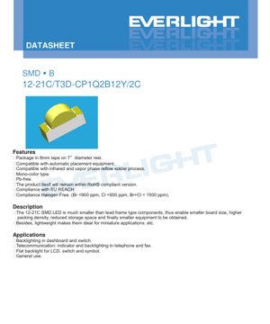
4. Mechanical and Package Information
4.1 Package Dimensions
The LED conforms to a standard SMD package with dimensions of approximately 2.0mm in length, 1.25mm in width, and 0.8mm in height (tolerance ±0.1mm unless otherwise noted). The package drawing clearly indicates the cathode mark, which is essential for correct PCB orientation. The recommended land pattern (footprint) is provided to ensure proper soldering and mechanical stability.
4.2 Polarity Identification
Correct polarity is critical. The package features a distinct cathode mark. The datasheet includes a detailed diagram showing this identification. Installing the LED in reverse polarity will prevent it from illuminating and applying the absolute maximum reverse voltage of 5V could damage the device.
5. Soldering and Assembly Guidelines
Adherence to these guidelines is mandatory to prevent thermal or mechanical damage during the assembly process.
5.1 Reflow Soldering Profile
The component is compatible with lead-free (Pb-free) reflow soldering processes. The specified temperature profile is critical:
- Pre-heating: 150-200°C for 60-120 seconds.
- Time Above Liquidus (217°C): 60-150 seconds.
- Peak Temperature: 260°C maximum, held for no more than 10 seconds.
- Heating Rate: Maximum 6°C/second.
- Time Above 255°C: Maximum 30 seconds.
- Cooling Rate: Maximum 3°C/second.
5.2 Hand Soldering
If hand soldering is necessary, extreme care must be taken. The soldering iron tip temperature must be below 350°C, and contact time per terminal must not exceed 3 seconds. A low-capacity iron (≤25W) is recommended. A minimum interval of 2 seconds should be observed between soldering each terminal to allow for cooling.
5.3 Storage and Moisture Sensitivity
The LEDs are packaged in moisture-resistant barrier bags with desiccant.
- Before Opening: Store at ≤30°C and ≤90% Relative Humidity (RH).
- After Opening (Floor Life): 168 hours (7 days) at ≤30°C and ≤60% RH.
- Baking: If the floor life is exceeded or the desiccant indicates moisture ingress, bake at 60 ±5°C for 24 hours before use.
6. Packaging and Ordering Information
6.1 Standard Packaging
The LEDs are supplied in 8mm carrier tape on 7-inch diameter reels. Each reel contains 2000 pieces. The carrier tape and reel dimensions are specified in the datasheet to facilitate automated handling and setup of pick-and-place machines.
6.2 Label Explanation
The reel label contains critical information for traceability and verification:
- CPN: Customer's Product Number.
- P/N: Manufacturer's Product Number (e.g., 12-21C/T3D-CP1Q2B12Y/2C).
- QTY: Packing Quantity.
- CAT: Luminous Intensity Rank (Bin Code: P1, P2, Q1, Q2).
- HUE: Chromaticity Coordinates & Dominant Wavelength Rank (Bin Code: 1, 2, 3, 4).
- REF: Forward Voltage Rank (Bin Code: 34 to 40).
- LOT No: Manufacturing Lot Number for traceability.
7. Application Design Considerations
7.1 Current Limiting is Mandatory
LEDs are current-driven devices. An external current-limiting resistor is absolutely required. The forward voltage has a negative temperature coefficient and a manufacturing spread (as seen in the binning). A slight increase in supply voltage or a decrease in VF due to temperature can cause a large, potentially destructive increase in forward current if no series resistor is used. The resistor value (R) can be calculated using Ohm's Law: R = (Vsupply - VF) / IF, where IF is the desired operating current (e.g., 5mA).
7.2 Thermal Management
While the power dissipation is low (40mW max), proper thermal design on the PCB is still important for longevity, especially in high ambient temperature applications. Ensure the PCB copper pad connected to the LED's thermal path (often the cathode) is sufficiently sized to act as a heat sink and is connected to larger copper planes if possible.
7.3 ESD Protection
\pWith an ESD rating of 150V (HBM), these devices are sensitive. Implement ESD control measures throughout handling, storage, and assembly. This includes the use of grounded workstations, wrist straps, and conductive containers.
8. Technical Comparison and Differentiation
Compared to larger, through-hole LEDs, the 12-21C offers a drastic reduction in size and weight, enabling modern miniaturized designs. Its wide 110-degree viewing angle, provided by the diffused yellow resin, offers more uniform light emission compared to clear resin packages with narrower beams, making it superior for area illumination and backlighting. The comprehensive binning system for intensity, voltage, and color provides a level of consistency that is essential for professional applications where visual uniformity is paramount, setting it apart from non-binned or loosely binned commodity LEDs.
9. Frequently Asked Questions (FAQ)
9.1 Can I drive this LED without a current-limiting resistor?
No. This is explicitly warned against in the "Precautions For Use" section. The LED is highly sensitive to voltage changes. Operating it directly from a voltage source, even a regulated one, is very likely to cause immediate failure due to overcurrent.
9.2 What is the difference between the P1, Q2, etc., bins?
These are luminous intensity bins. P1 represents the lowest brightness group (45.0-57.0 mcd), and Q2 represents the highest (90.0-112.0 mcd) when tested at 5mA. For consistent appearance in an array, all LEDs should be from the same intensity bin.
9.3 How many times can I reflow solder this component?
The datasheet specifies that reflow soldering should not be done more than two times. Each reflow cycle subjects the component to thermal stress, and exceeding two cycles may compromise the internal wire bonds or the epoxy resin.
9.4 The bag has been open for a week. Can I still use the LEDs?
Possibly, but they require baking first. The floor life after opening is 168 hours (7 days) under specified conditions. If this time is exceeded, you must perform the baking procedure (60 ±5°C for 24 hours) to drive out absorbed moisture and prevent "popcorning" or delamination during subsequent soldering.
10. Practical Design and Usage Case
Scenario: Designing a backlit membrane switch panel. A designer needs 20 white LEDs for even backlighting of icons. They would:
- Select Bin: Choose all LEDs from the same Luminous Intensity bin (e.g., Q1) and Chromaticity bin (e.g., 2) to ensure uniform brightness and color.
- Calculate Resistor: Using a 5V supply and a nominal VF of 3.0V (from Bin 36), target IF = 5mA. R = (5V - 3.0V) / 0.005A = 400Ω. A standard 390Ω or 430Ω resistor would be suitable.
- PCB Layout: Use the recommended land pattern from the datasheet. Connect the cathode pad to a slightly larger copper pour for minor heat sinking.
- Assembly: Keep components in sealed bag until ready. Use the specified lead-free reflow profile. Avoid hand soldering if possible.
- Testing: Verify forward voltage and light output of a sample from the batch to confirm it aligns with the selected bin.
11. Operational Principle
The 12-21C LED is based on an InGaN (Indium Gallium Nitride) semiconductor chip. When a forward voltage exceeding the diode's junction potential (VF) is applied, electrons and holes are injected into the active region of the semiconductor. Their recombination releases energy in the form of photons, a process called electroluminescence. The specific composition of the InGaN layers determines the wavelength of the emitted light, producing the "Pure White" spectrum specified. The yellow diffused resin encapsulant serves to protect the chip, shape the light output into a wide viewing angle, and may contain phosphors (though not explicitly stated for this "Pure White" type, it is common for white LEDs to use a blue chip with a yellow phosphor).
12. Industry Trends and Context
The 12-21C exemplifies key trends in LED technology: relentless miniaturization, increased efficiency (higher luminous intensity from a small package), and enhanced manufacturability via SMD packaging and tape-and-reel supply. The focus on environmental compliance (RoHS, Halogen-Free) reflects broader industry and regulatory demands. The detailed binning system highlights the market's need for predictable, consistent performance in mass-produced electronics. Future evolution in this product category would likely focus on further increasing luminous efficacy (more light per mA), improving color rendering index (CRI) for white LEDs, and perhaps integrating driver circuitry or multiple dice into similarly sized packages for smarter, more functional lighting solutions.
LED Specification Terminology
Complete explanation of LED technical terms
Photoelectric Performance
| Term | Unit/Representation | Simple Explanation | Why Important |
|---|---|---|---|
| Luminous Efficacy | lm/W (lumens per watt) | Light output per watt of electricity, higher means more energy efficient. | Directly determines energy efficiency grade and electricity cost. |
| Luminous Flux | lm (lumens) | Total light emitted by source, commonly called "brightness". | Determines if the light is bright enough. |
| Viewing Angle | ° (degrees), e.g., 120° | Angle where light intensity drops to half, determines beam width. | Affects illumination range and uniformity. |
| CCT (Color Temperature) | K (Kelvin), e.g., 2700K/6500K | Warmth/coolness of light, lower values yellowish/warm, higher whitish/cool. | Determines lighting atmosphere and suitable scenarios. |
| CRI / Ra | Unitless, 0–100 | Ability to render object colors accurately, Ra≥80 is good. | Affects color authenticity, used in high-demand places like malls, museums. |
| SDCM | MacAdam ellipse steps, e.g., "5-step" | Color consistency metric, smaller steps mean more consistent color. | Ensures uniform color across same batch of LEDs. |
| Dominant Wavelength | nm (nanometers), e.g., 620nm (red) | Wavelength corresponding to color of colored LEDs. | Determines hue of red, yellow, green monochrome LEDs. |
| Spectral Distribution | Wavelength vs intensity curve | Shows intensity distribution across wavelengths. | Affects color rendering and quality. |
Electrical Parameters
| Term | Symbol | Simple Explanation | Design Considerations |
|---|---|---|---|
| Forward Voltage | Vf | Minimum voltage to turn on LED, like "starting threshold". | Driver voltage must be ≥Vf, voltages add up for series LEDs. |
| Forward Current | If | Current value for normal LED operation. | Usually constant current drive, current determines brightness & lifespan. |
| Max Pulse Current | Ifp | Peak current tolerable for short periods, used for dimming or flashing. | Pulse width & duty cycle must be strictly controlled to avoid damage. |
| Reverse Voltage | Vr | Max reverse voltage LED can withstand, beyond may cause breakdown. | Circuit must prevent reverse connection or voltage spikes. |
| Thermal Resistance | Rth (°C/W) | Resistance to heat transfer from chip to solder, lower is better. | High thermal resistance requires stronger heat dissipation. |
| ESD Immunity | V (HBM), e.g., 1000V | Ability to withstand electrostatic discharge, higher means less vulnerable. | Anti-static measures needed in production, especially for sensitive LEDs. |
Thermal Management & Reliability
| Term | Key Metric | Simple Explanation | Impact |
|---|---|---|---|
| Junction Temperature | Tj (°C) | Actual operating temperature inside LED chip. | Every 10°C reduction may double lifespan; too high causes light decay, color shift. |
| Lumen Depreciation | L70 / L80 (hours) | Time for brightness to drop to 70% or 80% of initial. | Directly defines LED "service life". |
| Lumen Maintenance | % (e.g., 70%) | Percentage of brightness retained after time. | Indicates brightness retention over long-term use. |
| Color Shift | Δu′v′ or MacAdam ellipse | Degree of color change during use. | Affects color consistency in lighting scenes. |
| Thermal Aging | Material degradation | Deterioration due to long-term high temperature. | May cause brightness drop, color change, or open-circuit failure. |
Packaging & Materials
| Term | Common Types | Simple Explanation | Features & Applications |
|---|---|---|---|
| Package Type | EMC, PPA, Ceramic | Housing material protecting chip, providing optical/thermal interface. | EMC: good heat resistance, low cost; Ceramic: better heat dissipation, longer life. |
| Chip Structure | Front, Flip Chip | Chip electrode arrangement. | Flip chip: better heat dissipation, higher efficacy, for high-power. |
| Phosphor Coating | YAG, Silicate, Nitride | Covers blue chip, converts some to yellow/red, mixes to white. | Different phosphors affect efficacy, CCT, and CRI. |
| Lens/Optics | Flat, Microlens, TIR | Optical structure on surface controlling light distribution. | Determines viewing angle and light distribution curve. |
Quality Control & Binning
| Term | Binning Content | Simple Explanation | Purpose |
|---|---|---|---|
| Luminous Flux Bin | Code e.g., 2G, 2H | Grouped by brightness, each group has min/max lumen values. | Ensures uniform brightness in same batch. |
| Voltage Bin | Code e.g., 6W, 6X | Grouped by forward voltage range. | Facilitates driver matching, improves system efficiency. |
| Color Bin | 5-step MacAdam ellipse | Grouped by color coordinates, ensuring tight range. | Guarantees color consistency, avoids uneven color within fixture. |
| CCT Bin | 2700K, 3000K etc. | Grouped by CCT, each has corresponding coordinate range. | Meets different scene CCT requirements. |
Testing & Certification
| Term | Standard/Test | Simple Explanation | Significance |
|---|---|---|---|
| LM-80 | Lumen maintenance test | Long-term lighting at constant temperature, recording brightness decay. | Used to estimate LED life (with TM-21). |
| TM-21 | Life estimation standard | Estimates life under actual conditions based on LM-80 data. | Provides scientific life prediction. |
| IESNA | Illuminating Engineering Society | Covers optical, electrical, thermal test methods. | Industry-recognized test basis. |
| RoHS / REACH | Environmental certification | Ensures no harmful substances (lead, mercury). | Market access requirement internationally. |
| ENERGY STAR / DLC | Energy efficiency certification | Energy efficiency and performance certification for lighting. | Used in government procurement, subsidy programs, enhances competitiveness. |