Table of Contents
- 1. Product Overview
- 1.1 Key Features and Compliance
- 1.2 Target Applications
- 2. Technical Parameters: In-Depth Objective Interpretation
- 2.1 Absolute Maximum Ratings
- 2.2 Electro-Optical Characteristics
- 2.3 Thermal Considerations
- 3. Binning System Explanation
- 3.1 Luminous Intensity Binning
- 3.2 Dominant Wavelength Binning
- 3.3 Forward Voltage Binning
- 4. Performance Curve Analysis
- 5. Mechanical and Package Information
- 5.1 Package Dimensions
- 5.2 Polarity Identification
- 6. Soldering and Assembly Guidelines
- 6.1 Reflow Soldering Profile
- 6.2 Hand Soldering Instructions
- 6.3 Storage and Moisture Sensitivity
- 7. Packaging and Ordering Information
- 7.1 Reel and Tape Specifications
- 7.2 Label Explanation
- 7.3 Moisture-Resistant Packaging
- 8. Application Design Recommendations
- 8.1 Current Limiting and Protection
- 8.2 PCB Layout Considerations
- 8.3 Application Restrictions
- 9. Technical Comparison and Differentiation
- 10. Frequently Asked Questions (FAQ)
- 11. Practical Design and Usage Case
- 12. Operating Principle Introduction
- 13. Technology Trends and Developments
- LED Specification Terminology
- Photoelectric Performance
- Electrical Parameters
- Thermal Management & Reliability
- Packaging & Materials
- Quality Control & Binning
- Testing & Certification
1. Product Overview
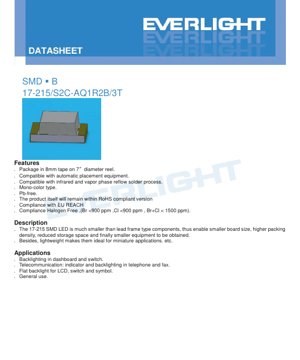
This document provides the complete technical specifications for the 17-215/S2C-AQ1R2B/3T surface-mount device (SMD) light-emitting diode (LED). This component is a mono-color type, emitting a brilliant orange light, and is constructed using AlGaInP semiconductor material encapsulated in a water-clear resin. Its primary design advantage is its compact form factor, which enables significant reductions in printed circuit board (PCB) size, allows for higher component packing density, minimizes required storage space, and ultimately contributes to the development of smaller end-user equipment. The lightweight nature of the package further makes it an ideal choice for miniature and space-constrained applications.
1.1 Key Features and Compliance
The LED is supplied on 8mm tape wound onto 7-inch diameter reels, ensuring compatibility with standard automated pick-and-place assembly equipment. It is designed for use with both infrared and vapor phase reflow soldering processes, facilitating integration into modern manufacturing lines. The product is manufactured as a Pb-free component and remains compliant with the Restriction of Hazardous Substances (RoHS) directive. It also complies with EU REACH regulations and meets halogen-free requirements, with bromine (Br) and chlorine (Cl) content each below 900 ppm and their combined total below 1500 ppm.
1.2 Target Applications
This LED is suited for a variety of indicator and backlighting functions. Common application areas include backlighting for automotive dashboards and switches, status indicators and keypad backlighting in telecommunication devices such as telephones and fax machines, flat backlighting units for liquid crystal displays (LCDs), and general-purpose indicator use where a brilliant orange signal is required.
2. Technical Parameters: In-Depth Objective Interpretation
2.1 Absolute Maximum Ratings
The absolute maximum ratings define the stress limits beyond which permanent damage to the device may occur. These values are specified at an ambient temperature (Ta) of 25°C and must not be exceeded under any operating conditions. The maximum reverse voltage (VR) is 5V. The maximum continuous forward current (IF) is 25 mA. For pulsed operation, a peak forward current (IFP) of 60 mA is permissible under a duty cycle of 1/10 at 1 kHz. The maximum power dissipation (Pd) is 60 mW. The device can withstand an electrostatic discharge (ESD) of 2000V per the Human Body Model (HBM). The operating temperature range (Topr) is from -40°C to +85°C, while the storage temperature range (Tstg) is slightly wider, from -40°C to +90°C. For soldering, the component can endure reflow profiles with a peak temperature of 260°C for up to 10 seconds, or hand soldering with an iron tip temperature of 350°C for a maximum of 3 seconds per terminal.
2.2 Electro-Optical Characteristics
The electro-optical characteristics are the core performance parameters, measured at Ta=25°C and a standard test current of IF=20 mA. The luminous intensity (Iv) has a typical range, with specific minimum and maximum values defined by the binning system. The viewing angle (2θ1/2), where the luminous intensity is half of the on-axis value, is typically 130 degrees, providing a wide emission pattern. The light output is characterized by its spectral properties: the peak wavelength (λp) is typically 611 nm, while the dominant wavelength (λd) ranges between 600.5 nm and 612.5 nm depending on the bin. The spectral bandwidth (Δλ) is typically 17 nm. The electrical characteristic is defined by the forward voltage (VF), which ranges from 1.75V to 2.35V. The reverse current (IR) is guaranteed to be 10 μA or less when a reverse voltage of 5V is applied, noting that the device is not designed for operation in reverse bias.
2.3 Thermal Considerations
While not explicitly detailed in a separate section, thermal management is implicit in the specifications. The maximum power dissipation of 60 mW and the operating temperature range up to +85°C define the thermal operating window. Designers must ensure that the junction temperature does not exceed its maximum limit, which is influenced by the PCB layout, copper area, and ambient conditions. Proper heat sinking through the PCB pads is essential for maintaining long-term reliability and preventing luminous output degradation.
3. Binning System Explanation
The product is sorted into bins based on three key parameters to ensure consistency within a production lot and allow designers to select components matching their specific tolerance requirements.
3.1 Luminous Intensity Binning
Luminous intensity is categorized into four bin codes: Q1, Q2, R1, and R2. The Q1 bin covers intensities from 72.00 mcd to 90.00 mcd. Q2 ranges from 90.00 mcd to 112.00 mcd. R1 spans 112.00 mcd to 140.00 mcd. The highest output bin, R2, includes LEDs from 140.00 mcd to 180.00 mcd. A tolerance of ±11% applies within each bin.
3.2 Dominant Wavelength Binning
The dominant wavelength, which correlates with perceived color, is binned into four codes: D8, D9, D10, and D11. D8 covers 600.50 nm to 603.50 nm. D9 covers 603.50 nm to 606.50 nm. D10 covers 606.50 nm to 609.50 nm. D11 covers 609.50 nm to 612.50 nm. A tight tolerance of ±1 nm is maintained within each bin.
3.3 Forward Voltage Binning
Forward voltage is sorted into three bins to aid in current regulation design. Bin 0 covers 1.75V to 1.95V. Bin 1 covers 1.95V to 2.15V. Bin 2 covers 2.15V to 2.35V. A tolerance of ±0.1V is specified for each bin.
4. Performance Curve Analysis
The datasheet references typical electro-optical characteristic curves. While the specific graphs are not provided in the text, standard curves for such LEDs would typically include the relationship between forward current (IF) and forward voltage (VF), showing the diode's exponential IV characteristic. Another crucial curve would depict the relative luminous intensity as a function of forward current, illustrating how light output increases with current up to the maximum rating. A third important graph would show the variation of luminous intensity with ambient temperature, typically demonstrating a decrease in output as temperature rises. Finally, a spectral distribution graph would show the relative radiant power as a function of wavelength, centered around the 611 nm peak, with the 17 nm bandwidth clearly visible. These curves are essential for designers to predict performance under non-standard test conditions.
5. Mechanical and Package Information
5.1 Package Dimensions
The LED is housed in a standard SMD package. The key dimensions (in millimeters) are as follows, with a general tolerance of ±0.1mm unless otherwise specified: The overall package length is 2.0 mm. The width is 1.25 mm. The height is 0.8 mm. The cathode identifier is typically a notch or a green marking on the package. The detailed drawing includes pad spacing (e.g., 1.5 mm between pad centers) and land pattern recommendations to ensure proper soldering and mechanical stability.
5.2 Polarity Identification
Correct polarity is critical for operation. The package incorporates a visual marker, such as a chamfered corner or a colored dot, to identify the cathode terminal. Designers must align this marker with the corresponding cathode pad on the PCB layout to prevent reverse connection, which could lead to immediate failure or degraded performance if the maximum reverse voltage is exceeded.
6. Soldering and Assembly Guidelines
6.1 Reflow Soldering Profile
For Pb-free reflow soldering, a specific temperature profile must be followed. The pre-heating zone should ramp from ambient to between 150°C and 200°C over 60 to 120 seconds. The critical reflow zone requires the temperature to be above 217°C (the melting point of typical Pb-free solder) for 60 to 150 seconds, with the peak temperature not exceeding 260°C for more than 10 seconds. The maximum ramp-up rate to peak should be 6°C per second, and the time above 255°C should be limited to 30 seconds maximum. The cool-down rate should not exceed 3°C per second. Reflow soldering should not be performed more than two times on the same component.
6.2 Hand Soldering Instructions
If hand soldering is necessary, extreme care is required. The soldering iron tip temperature must be below 350°C. Contact time for each terminal must be limited to 3 seconds or less. The soldering iron power should be 25W or less. An interval of at least 2 seconds should be left between soldering the two terminals to prevent excessive heat buildup. It is strongly advised to use a double-head soldering iron for any repair work to simultaneously heat both terminals and avoid mechanical stress.
6.3 Storage and Moisture Sensitivity
This component is moisture-sensitive. The moisture-proof bag must not be opened until the parts are ready for use. After opening, unused LEDs must be stored in an environment of 30°C or less and 60% relative humidity (RH) or less. The "floor life" after bag opening is 168 hours (7 days). If this time is exceeded or if the moisture indicator (silica gel) has changed color, the components must be baked at 60°C ±5°C for 24 hours before use to remove absorbed moisture and prevent "popcorning" during reflow.
7. Packaging and Ordering Information
7.1 Reel and Tape Specifications
The LEDs are packaged in embossed carrier tape with a width of 8 mm. The tape is wound onto a standard 7-inch (178 mm) diameter reel. Each reel contains 3000 pieces. Detailed dimensions for the reel, including hub diameter and flange width, are provided, as are the precise dimensions of the carrier tape pockets and cover tape.
7.2 Label Explanation
The reel label contains critical information for traceability and identification: CPN (Customer's Product Number), P/N (Manufacturer's Product Number, e.g., 17-215/S2C-AQ1R2B/3T), QTY (Packing Quantity), CAT (Luminous Intensity Rank/bin), HUE (Chromaticity Coordinates & Dominant Wavelength Rank/bin), REF (Forward Voltage Rank/bin), and LOT No (Manufacturing Lot Number for traceability).
7.3 Moisture-Resistant Packaging
The reel is sealed inside an aluminum laminate moisture-proof bag along with a desiccant packet and a humidity indicator card. This packaging ensures the components remain dry during shipping and storage until the point of use.
8. Application Design Recommendations
8.1 Current Limiting and Protection
An external current-limiting resistor is mandatory for safe operation. The LED's forward voltage has a negative temperature coefficient and a manufacturing tolerance. A slight increase in supply voltage or a decrease in VF can cause a large, potentially destructive increase in forward current. The resistor value must be calculated based on the supply voltage (Vs), the maximum forward voltage (VF_max from the bin) at the desired current, and the target forward current (IF, not to exceed 25 mA continuous). The formula is R = (Vs - VF) / IF. Using the minimum VF for calculation ensures the current does not exceed the limit under worst-case conditions.
8.2 PCB Layout Considerations
The PCB land pattern should match the recommended footprint to ensure proper solder fillet formation and mechanical strength. Adequate copper area connected to the thermal pads (if any) or the anode/cathode traces helps dissipate heat. Avoid placing the LED near other significant heat sources. Ensure the polarity marking on the PCB silkscreen clearly matches the package marking.
8.3 Application Restrictions
This standard commercial-grade LED is not specifically designed or qualified for high-reliability applications where failure could lead to serious injury or loss. This includes, but is not limited to, military and aerospace systems, automotive safety and security systems (e.g., airbags, braking), and life-supporting medical equipment. For such applications, components with appropriate automotive or medical qualifications must be sourced. The specifications in this document guarantee performance only when the device is used within the stated absolute maximum ratings and recommended operating conditions.
9. Technical Comparison and Differentiation
Compared to traditional leaded LEDs, this SMD type offers significant advantages: a much smaller footprint enabling higher density layouts, suitability for automated assembly reducing labor costs, and better thermal coupling to the PCB via the solder joints. Within the SMD orange LED segment, this specific part is differentiated by its use of AlGaInP technology, which typically offers higher efficiency and better color purity than older technologies like GaAsP for orange/red colors. The wide 130-degree viewing angle makes it suitable for applications requiring broad visibility, as opposed to narrow-angle LEDs used for focused illumination. Its compliance with halogen-free and RoHS standards aligns it with modern environmental regulations.
10. Frequently Asked Questions (FAQ)
Q: What is the difference between peak wavelength and dominant wavelength?
A: Peak wavelength (λp) is the wavelength at which the emitted optical power is maximum. Dominant wavelength (λd) is the single wavelength of monochromatic light that matches the perceived color of the LED's output. For LEDs with a symmetric spectrum, they are often close, but λd is more relevant for color-based applications.
Q: Can I drive this LED without a current-limiting resistor if I use a constant voltage source equal to its typical VF?
A: No. This is extremely dangerous and will likely destroy the LED. The VF has tolerance and varies with temperature. A so-called "constant" voltage source must have an output impedance that actively limits current, which is effectively what a series resistor does.
Q: Why is the storage temperature range wider than the operating range?
A: The operating range considers active electrical and thermal stresses that can accelerate failure mechanisms. The storage range is for passive components where only material stability and moisture ingress are primary concerns, allowing for a slightly wider temperature window.
Q: What happens if I exceed the 7-day floor life after opening the bag?
A: The component absorbs moisture from the air. During reflow soldering, this moisture can rapidly vaporize, causing internal delamination or cracking ("popcorning"), leading to immediate or latent failure. Baking as specified is required to drive out this moisture.
11. Practical Design and Usage Case
Case: Designing a status indicator panel with uniform brightness. A designer needs 20 orange indicators on a control panel. To ensure visual uniformity, they should specify LEDs from the same luminous intensity bin (e.g., all R1) and the same dominant wavelength bin (e.g., all D10). They plan to use a 5V supply. Selecting the worst-case VF_max of 2.35V from bin 2 and a target current of 20 mA, the series resistor value is R = (5V - 2.35V) / 0.020A = 132.5 Ohms. The nearest standard value is 130 Ohms. The power dissipated in the resistor is (5V-2.35V)*0.02A = 0.053W, so a standard 1/8W (0.125W) resistor is sufficient. The PCB layout should use the recommended land pattern, and all LEDs should be placed on the board and soldered in a single reflow pass to ensure consistent thermal history.
12. Operating Principle Introduction
Light emission in this LED is based on the principle of electroluminescence in a semiconductor p-n junction made of Aluminum Gallium Indium Phosphide (AlGaInP). When a forward voltage exceeding the junction's built-in potential is applied, electrons from the n-type region and holes from the p-type region are injected into the active region. There, electrons recombine with holes, releasing energy. In a direct bandgap semiconductor like AlGaInP, a significant portion of this energy is released as photons (light). The specific composition of the AlGaInP alloy determines the bandgap energy, which directly dictates the wavelength (color) of the emitted light. For brilliant orange, the bandgap corresponds to photons with a wavelength around 611 nm. The water-clear epoxy resin encapsulant protects the semiconductor chip, provides mechanical support, and shapes the light output beam.
13. Technology Trends and Developments
The general trend in SMD LEDs is toward higher luminous efficacy (more light output per electrical watt), improved color consistency through tighter binning, and increased reliability under higher temperature and current conditions. Packaging continues to evolve for better thermal management, allowing for higher drive currents in smaller footprints. There is also a drive toward broader spectral options within a single package platform. Furthermore, integration with onboard control electronics (e.g., constant current drivers, PWM controllers) into LED packages is a growing trend, simplifying circuit design for the end user. Environmental compliance, such as halogen-free materials and further reduction of hazardous substances, remains a key development driver across the industry.
LED Specification Terminology
Complete explanation of LED technical terms
Photoelectric Performance
| Term | Unit/Representation | Simple Explanation | Why Important |
|---|---|---|---|
| Luminous Efficacy | lm/W (lumens per watt) | Light output per watt of electricity, higher means more energy efficient. | Directly determines energy efficiency grade and electricity cost. |
| Luminous Flux | lm (lumens) | Total light emitted by source, commonly called "brightness". | Determines if the light is bright enough. |
| Viewing Angle | ° (degrees), e.g., 120° | Angle where light intensity drops to half, determines beam width. | Affects illumination range and uniformity. |
| CCT (Color Temperature) | K (Kelvin), e.g., 2700K/6500K | Warmth/coolness of light, lower values yellowish/warm, higher whitish/cool. | Determines lighting atmosphere and suitable scenarios. |
| CRI / Ra | Unitless, 0–100 | Ability to render object colors accurately, Ra≥80 is good. | Affects color authenticity, used in high-demand places like malls, museums. |
| SDCM | MacAdam ellipse steps, e.g., "5-step" | Color consistency metric, smaller steps mean more consistent color. | Ensures uniform color across same batch of LEDs. |
| Dominant Wavelength | nm (nanometers), e.g., 620nm (red) | Wavelength corresponding to color of colored LEDs. | Determines hue of red, yellow, green monochrome LEDs. |
| Spectral Distribution | Wavelength vs intensity curve | Shows intensity distribution across wavelengths. | Affects color rendering and quality. |
Electrical Parameters
| Term | Symbol | Simple Explanation | Design Considerations |
|---|---|---|---|
| Forward Voltage | Vf | Minimum voltage to turn on LED, like "starting threshold". | Driver voltage must be ≥Vf, voltages add up for series LEDs. |
| Forward Current | If | Current value for normal LED operation. | Usually constant current drive, current determines brightness & lifespan. |
| Max Pulse Current | Ifp | Peak current tolerable for short periods, used for dimming or flashing. | Pulse width & duty cycle must be strictly controlled to avoid damage. |
| Reverse Voltage | Vr | Max reverse voltage LED can withstand, beyond may cause breakdown. | Circuit must prevent reverse connection or voltage spikes. |
| Thermal Resistance | Rth (°C/W) | Resistance to heat transfer from chip to solder, lower is better. | High thermal resistance requires stronger heat dissipation. |
| ESD Immunity | V (HBM), e.g., 1000V | Ability to withstand electrostatic discharge, higher means less vulnerable. | Anti-static measures needed in production, especially for sensitive LEDs. |
Thermal Management & Reliability
| Term | Key Metric | Simple Explanation | Impact |
|---|---|---|---|
| Junction Temperature | Tj (°C) | Actual operating temperature inside LED chip. | Every 10°C reduction may double lifespan; too high causes light decay, color shift. |
| Lumen Depreciation | L70 / L80 (hours) | Time for brightness to drop to 70% or 80% of initial. | Directly defines LED "service life". |
| Lumen Maintenance | % (e.g., 70%) | Percentage of brightness retained after time. | Indicates brightness retention over long-term use. |
| Color Shift | Δu′v′ or MacAdam ellipse | Degree of color change during use. | Affects color consistency in lighting scenes. |
| Thermal Aging | Material degradation | Deterioration due to long-term high temperature. | May cause brightness drop, color change, or open-circuit failure. |
Packaging & Materials
| Term | Common Types | Simple Explanation | Features & Applications |
|---|---|---|---|
| Package Type | EMC, PPA, Ceramic | Housing material protecting chip, providing optical/thermal interface. | EMC: good heat resistance, low cost; Ceramic: better heat dissipation, longer life. |
| Chip Structure | Front, Flip Chip | Chip electrode arrangement. | Flip chip: better heat dissipation, higher efficacy, for high-power. |
| Phosphor Coating | YAG, Silicate, Nitride | Covers blue chip, converts some to yellow/red, mixes to white. | Different phosphors affect efficacy, CCT, and CRI. |
| Lens/Optics | Flat, Microlens, TIR | Optical structure on surface controlling light distribution. | Determines viewing angle and light distribution curve. |
Quality Control & Binning
| Term | Binning Content | Simple Explanation | Purpose |
|---|---|---|---|
| Luminous Flux Bin | Code e.g., 2G, 2H | Grouped by brightness, each group has min/max lumen values. | Ensures uniform brightness in same batch. |
| Voltage Bin | Code e.g., 6W, 6X | Grouped by forward voltage range. | Facilitates driver matching, improves system efficiency. |
| Color Bin | 5-step MacAdam ellipse | Grouped by color coordinates, ensuring tight range. | Guarantees color consistency, avoids uneven color within fixture. |
| CCT Bin | 2700K, 3000K etc. | Grouped by CCT, each has corresponding coordinate range. | Meets different scene CCT requirements. |
Testing & Certification
| Term | Standard/Test | Simple Explanation | Significance |
|---|---|---|---|
| LM-80 | Lumen maintenance test | Long-term lighting at constant temperature, recording brightness decay. | Used to estimate LED life (with TM-21). |
| TM-21 | Life estimation standard | Estimates life under actual conditions based on LM-80 data. | Provides scientific life prediction. |
| IESNA | Illuminating Engineering Society | Covers optical, electrical, thermal test methods. | Industry-recognized test basis. |
| RoHS / REACH | Environmental certification | Ensures no harmful substances (lead, mercury). | Market access requirement internationally. |
| ENERGY STAR / DLC | Energy efficiency certification | Energy efficiency and performance certification for lighting. | Used in government procurement, subsidy programs, enhances competitiveness. |