Table of Contents
- 1. Product Overview
- 2. In-Depth Technical Parameter Analysis
- 2.1 Absolute Maximum Ratings
- 2.2 Electro-Optical Characteristics
- 3. Binning System Explanation
- 3.1 Luminous Intensity Binning
- 3.2 Dominant Wavelength Binning
- 3.3 Forward Voltage Binning
- 4. Performance Curve Analysis The datasheet references typical electro-optical characteristic curves. While specific graphs are not detailed in the provided text, such curves typically illustrate the relationship between forward current and luminous intensity, forward voltage versus temperature, and the spectral power distribution. Analyzing these curves is crucial for understanding performance under non-standard conditions, such as different drive currents or ambient temperatures, which affect output brightness and device longevity. 5. Mechanical and Package Information
- 5.1 Package Dimensions
- 5.2 Polarity Identification
- 6. Soldering and Assembly Guidelines
- 6.1 Reflow Soldering Profile
- 6.2 Hand Soldering
- 6.3 Storage and Handling
- 7. Packaging and Ordering Information
- 8. Application Recommendations
- 8.1 Typical Application Scenarios
- 8.2 Critical Design Considerations
- 9. Technical Comparison and Differentiation
- 10. Frequently Asked Questions (FAQs)
- 11. Practical Application Case Study
- 12. Operating Principle
- 13. Technology Trends
1. Product Overview
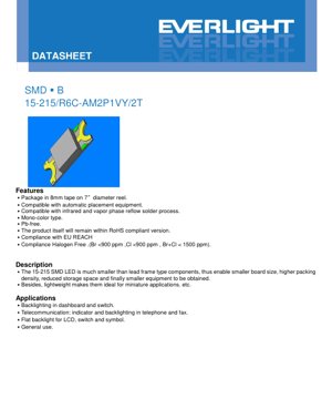
The 15-215 is a surface-mount device (SMD) LED designed for high-density electronic assemblies. Its primary emitted color is brilliant red, achieved using an AlGaInP chip encased in a water-clear resin package. The core advantages of this component include its miniature footprint, compatibility with automated assembly processes, and compliance with modern environmental and safety standards such as RoHS, REACH, and halogen-free requirements.
The product is targeted at applications requiring reliable, compact indicator lighting or backlighting. Its small size enables significant reductions in PCB area and final product dimensions, while its lightweight construction makes it suitable for portable and miniature devices.
2. In-Depth Technical Parameter Analysis
2.1 Absolute Maximum Ratings
Operating the device beyond these limits may cause permanent damage. Key ratings include a maximum reverse voltage (VR) of 5V and a continuous forward current (IF) of 25mA. The device can withstand a peak forward current (IFP) of 60mA under pulsed conditions (1/10 duty cycle @ 1kHz). The maximum power dissipation (Pd) is 60mW. The operating temperature range is specified from -40°C to +85°C, with a slightly wider storage temperature range of -40°C to +90°C. The component is rated for reflow soldering at 260°C for 10 seconds.
2.2 Electro-Optical Characteristics
Measured at a standard test current of 5mA and an ambient temperature of 25°C, the key performance parameters are defined. The luminous intensity (Iv) has a typical range, with specific minimum and maximum values defined in the binning tables. The device features a very wide viewing angle (2θ1/2) of 140 degrees, providing broad, even illumination. The dominant wavelength (λd) falls within the red spectrum, specifically between 617.5 nm and 633.5 nm, with a typical peak wavelength (λp) around 632 nm. The forward voltage (VF) is relatively low, ranging from 1.70V to 2.20V at 5mA, contributing to energy efficiency.
3. Binning System Explanation
The product is classified into bins to ensure consistency in key parameters. This allows designers to select components that meet specific application requirements for brightness, color, and electrical behavior.
3.1 Luminous Intensity Binning
Luminous intensity is categorized into four bins: M2, N1, N2, and P1. The P1 bin represents the highest brightness group, with intensities ranging from 45.0 mcd to 57.0 mcd at 5mA. A tolerance of ±11% applies within each bin.
3.2 Dominant Wavelength Binning
The color, defined by dominant wavelength, is sorted into four bins: E4, E5, E6, and E7. Bin E4 covers the shorter wavelength reds (617.5-621.5 nm), while bin E7 covers the longer wavelength reds (629.5-633.5 nm). The tolerance is ±1nm.
3.3 Forward Voltage Binning
Forward voltage is binned into four groups: 19, 20, 21, and 22. For example, bin 19 covers VF from 1.70V to 1.80V. This binning helps in designing consistent current drive circuits, especially when using multiple LEDs in series. The tolerance is ±0.05V.
4. Performance Curve Analysis
The datasheet references typical electro-optical characteristic curves. While specific graphs are not detailed in the provided text, such curves typically illustrate the relationship between forward current and luminous intensity, forward voltage versus temperature, and the spectral power distribution. Analyzing these curves is crucial for understanding performance under non-standard conditions, such as different drive currents or ambient temperatures, which affect output brightness and device longevity.
5. Mechanical and Package Information
5.1 Package Dimensions
The LED has a compact SMD package. The key dimensions are approximately 2.0mm in length, 1.25mm in width, and 0.8mm in height (tolerance ±0.1mm). The package includes two anode and two cathode terminals for stable soldering.
5.2 Polarity Identification
The package features a polarity indicator, typically a notch or a chamfered corner, to ensure correct orientation during assembly. Incorrect placement will prevent the LED from illuminating and may subject it to reverse voltage stress.
6. Soldering and Assembly Guidelines
6.1 Reflow Soldering Profile
For Pb-free soldering, a specific temperature profile must be followed: pre-heating between 150-200°C for 60-120 seconds, a time above liquidus (217°C) of 60-150 seconds, and a peak temperature not exceeding 260°C for a maximum of 10 seconds. The maximum heating and cooling rates are also specified to prevent thermal shock. Reflow should not be performed more than twice.
6.2 Hand Soldering
If hand soldering is necessary, the iron tip temperature must be below 350°C, and contact time per terminal should not exceed 3 seconds. A low-power iron (≤25W) is recommended, with adequate cooling time between soldering each terminal to avoid overheating.
6.3 Storage and Handling
The components are packaged in moisture-resistant bags with desiccant. The bag should not be opened until the parts are ready for use. If the bag is opened, the LEDs have a "floor life" of one year under controlled conditions (≤30°C, ≤60% RH). Exceeded storage time or faded desiccant requires a baking pre-treatment at 60±5°C for 24 hours before use.
7. Packaging and Ordering Information
The LEDs are supplied on 8mm wide carrier tape, wound onto 7-inch diameter reels. Each reel contains 2000 pieces. The packaging includes labels with critical information: Product Number (P/N), quantity (QTY), and the specific bin codes for luminous intensity (CAT), dominant wavelength (HUE), and forward voltage (REF).
8. Application Recommendations
8.1 Typical Application Scenarios
This LED is well-suited for backlighting applications in automotive dashboards and switches, indicator and backlighting in telecommunication devices (phones, fax machines), flat backlighting for LCDs and symbols, and general-purpose status indication.
8.2 Critical Design Considerations
Current Limiting: An external current-limiting resistor is mandatory. LEDs are current-driven devices; a small change in forward voltage can cause a large change in current, potentially leading to immediate failure (burn-out). The resistor value must be calculated based on the supply voltage and the desired forward current (typically 5-20mA, not exceeding 25mA).
Thermal Management: While the package is small, ensuring adequate PCB copper area or thermal vias can help dissipate heat, especially when operating at higher currents or in elevated ambient temperatures, thereby maintaining performance and reliability.
ESD Protection: Although the device has a Human Body Model (HBM) ESD rating of 2000V, standard ESD precautions during handling and assembly are still recommended.
9. Technical Comparison and Differentiation
Compared to traditional leaded LEDs, the 15-215 SMD LED offers significant advantages in size, weight, and suitability for automated pick-and-place assembly, leading to lower manufacturing costs for high-volume production. Its wide viewing angle of 140 degrees provides more uniform light emission compared to narrower-angle devices, making it better for area illumination. The specific AlGaInP material system offers high efficiency and good color purity in the red spectrum.
10. Frequently Asked Questions (FAQs)
Q: Can I drive this LED directly from a 3.3V or 5V logic supply?
A: No. You must always use a series current-limiting resistor. The required resistor value (R) is calculated as R = (Vsupply - VF) / IF. For example, with a 5V supply, a VF of 2.0V, and a target IF of 20mA: R = (5 - 2) / 0.02 = 150 Ohms.
Q: What does the "water clear" resin color mean?
A: It means the encapsulating lens is transparent, not diffused or tinted. This allows the true color of the AlGaInP chip (brilliant red) to be seen directly, often resulting in a more saturated and intense color appearance.
Q: How do I interpret the part number 15-215/R6C-AM2P1VY/2T?
A: While the full decoding may be proprietary, segments typically indicate the series (15-215), possibly a color/brightness code (R6C), and specific bin codes (A, M2, P1, VY, 2T) corresponding to the luminous intensity, wavelength, and voltage bins described in the datasheet.
11. Practical Application Case Study
Scenario: Designing a status indicator panel for a network router.
The panel requires multiple bright red LEDs to indicate power, network activity, and system errors. The 15-215 LED in the P1 brightness bin is selected for high visibility. A design using a common 3.3V rail is chosen. Calculating for a conservative 15mA drive current and a typical VF of 1.9V (from bin 20), the resistor value is (3.3V - 1.9V) / 0.015A = 93.3 Ohms. A standard 100 Ohm resistor is selected, resulting in a forward current of approximately 14mA, which is within specification and provides ample brightness while ensuring long-term reliability. The wide 140-degree viewing angle ensures the status is visible from various angles around the device.
12. Operating Principle
This LED is a semiconductor light source. When a forward voltage exceeding its characteristic forward voltage (VF) is applied across the anode and cathode, electrons and holes recombine within the active region of the AlGaInP (Aluminum Gallium Indium Phosphide) semiconductor chip. This recombination process releases energy in the form of photons, with the specific bandgap of the AlGaInP material determining the wavelength of the emitted light, in this case, brilliant red. The water-clear epoxy resin lens serves to protect the semiconductor die, shape the light output beam, and enhance light extraction from the chip.
13. Technology Trends
The development of SMD LEDs like the 15-215 is part of the broader trend in electronics towards miniaturization, increased reliability, and automated manufacturing. Advancements in semiconductor materials, such as AlGaInP, have consistently improved luminous efficacy (light output per electrical input) and color stability over time and temperature. Future trends may focus on further efficiency gains, even smaller package sizes for ultra-high-density applications, and enhanced thermal performance to support higher drive currents in compact spaces. The industry also continues to emphasize environmental compliance, driving the elimination of hazardous substances and improving recyclability.
LED Specification Terminology
Complete explanation of LED technical terms
Photoelectric Performance
| Term | Unit/Representation | Simple Explanation | Why Important |
|---|---|---|---|
| Luminous Efficacy | lm/W (lumens per watt) | Light output per watt of electricity, higher means more energy efficient. | Directly determines energy efficiency grade and electricity cost. |
| Luminous Flux | lm (lumens) | Total light emitted by source, commonly called "brightness". | Determines if the light is bright enough. |
| Viewing Angle | ° (degrees), e.g., 120° | Angle where light intensity drops to half, determines beam width. | Affects illumination range and uniformity. |
| CCT (Color Temperature) | K (Kelvin), e.g., 2700K/6500K | Warmth/coolness of light, lower values yellowish/warm, higher whitish/cool. | Determines lighting atmosphere and suitable scenarios. |
| CRI / Ra | Unitless, 0–100 | Ability to render object colors accurately, Ra≥80 is good. | Affects color authenticity, used in high-demand places like malls, museums. |
| SDCM | MacAdam ellipse steps, e.g., "5-step" | Color consistency metric, smaller steps mean more consistent color. | Ensures uniform color across same batch of LEDs. |
| Dominant Wavelength | nm (nanometers), e.g., 620nm (red) | Wavelength corresponding to color of colored LEDs. | Determines hue of red, yellow, green monochrome LEDs. |
| Spectral Distribution | Wavelength vs intensity curve | Shows intensity distribution across wavelengths. | Affects color rendering and quality. |
Electrical Parameters
| Term | Symbol | Simple Explanation | Design Considerations |
|---|---|---|---|
| Forward Voltage | Vf | Minimum voltage to turn on LED, like "starting threshold". | Driver voltage must be ≥Vf, voltages add up for series LEDs. |
| Forward Current | If | Current value for normal LED operation. | Usually constant current drive, current determines brightness & lifespan. |
| Max Pulse Current | Ifp | Peak current tolerable for short periods, used for dimming or flashing. | Pulse width & duty cycle must be strictly controlled to avoid damage. |
| Reverse Voltage | Vr | Max reverse voltage LED can withstand, beyond may cause breakdown. | Circuit must prevent reverse connection or voltage spikes. |
| Thermal Resistance | Rth (°C/W) | Resistance to heat transfer from chip to solder, lower is better. | High thermal resistance requires stronger heat dissipation. |
| ESD Immunity | V (HBM), e.g., 1000V | Ability to withstand electrostatic discharge, higher means less vulnerable. | Anti-static measures needed in production, especially for sensitive LEDs. |
Thermal Management & Reliability
| Term | Key Metric | Simple Explanation | Impact |
|---|---|---|---|
| Junction Temperature | Tj (°C) | Actual operating temperature inside LED chip. | Every 10°C reduction may double lifespan; too high causes light decay, color shift. |
| Lumen Depreciation | L70 / L80 (hours) | Time for brightness to drop to 70% or 80% of initial. | Directly defines LED "service life". |
| Lumen Maintenance | % (e.g., 70%) | Percentage of brightness retained after time. | Indicates brightness retention over long-term use. |
| Color Shift | Δu′v′ or MacAdam ellipse | Degree of color change during use. | Affects color consistency in lighting scenes. |
| Thermal Aging | Material degradation | Deterioration due to long-term high temperature. | May cause brightness drop, color change, or open-circuit failure. |
Packaging & Materials
| Term | Common Types | Simple Explanation | Features & Applications |
|---|---|---|---|
| Package Type | EMC, PPA, Ceramic | Housing material protecting chip, providing optical/thermal interface. | EMC: good heat resistance, low cost; Ceramic: better heat dissipation, longer life. |
| Chip Structure | Front, Flip Chip | Chip electrode arrangement. | Flip chip: better heat dissipation, higher efficacy, for high-power. |
| Phosphor Coating | YAG, Silicate, Nitride | Covers blue chip, converts some to yellow/red, mixes to white. | Different phosphors affect efficacy, CCT, and CRI. |
| Lens/Optics | Flat, Microlens, TIR | Optical structure on surface controlling light distribution. | Determines viewing angle and light distribution curve. |
Quality Control & Binning
| Term | Binning Content | Simple Explanation | Purpose |
|---|---|---|---|
| Luminous Flux Bin | Code e.g., 2G, 2H | Grouped by brightness, each group has min/max lumen values. | Ensures uniform brightness in same batch. |
| Voltage Bin | Code e.g., 6W, 6X | Grouped by forward voltage range. | Facilitates driver matching, improves system efficiency. |
| Color Bin | 5-step MacAdam ellipse | Grouped by color coordinates, ensuring tight range. | Guarantees color consistency, avoids uneven color within fixture. |
| CCT Bin | 2700K, 3000K etc. | Grouped by CCT, each has corresponding coordinate range. | Meets different scene CCT requirements. |
Testing & Certification
| Term | Standard/Test | Simple Explanation | Significance |
|---|---|---|---|
| LM-80 | Lumen maintenance test | Long-term lighting at constant temperature, recording brightness decay. | Used to estimate LED life (with TM-21). |
| TM-21 | Life estimation standard | Estimates life under actual conditions based on LM-80 data. | Provides scientific life prediction. |
| IESNA | Illuminating Engineering Society | Covers optical, electrical, thermal test methods. | Industry-recognized test basis. |
| RoHS / REACH | Environmental certification | Ensures no harmful substances (lead, mercury). | Market access requirement internationally. |
| ENERGY STAR / DLC | Energy efficiency certification | Energy efficiency and performance certification for lighting. | Used in government procurement, subsidy programs, enhances competitiveness. |