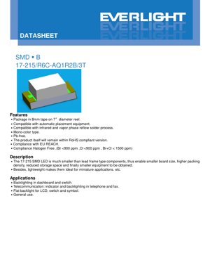
1. Product Overview
The 17-215 is a surface-mount device (SMD) LED designed for general indicator and backlighting applications. It utilizes an AIGaInP (Aluminum Gallium Indium Phosphide) chip to produce a brilliant red light output. This component is characterized by its compact size, which facilitates higher packing density on printed circuit boards (PCBs) and enables the design of smaller end-user equipment. The device is supplied on 8mm tape mounted on 7-inch diameter reels, making it fully compatible with standard automated pick-and-place assembly equipment.
1.1 Core Features and Compliance
The LED offers several key features that align with modern manufacturing and environmental standards. It is compatible with both infrared and vapor phase reflow soldering processes, which are common in high-volume electronics assembly. The product is constructed using lead-free (Pb-free) materials and is designed to remain compliant with the RoHS (Restriction of Hazardous Substances) directive. It also complies with EU REACH regulations and meets halogen-free requirements, with Bromine (Br) and Chlorine (Cl) content each below 900 ppm and their sum below 1500 ppm.
1.2 Target Applications
The primary application areas for this LED include backlighting for instrument panels, switches, and symbols. It is also suitable for use in telecommunication devices such as telephones and fax machines for status indication and keypad backlighting. Furthermore, it can be used for flat backlighting in LCDs and for general-purpose indicator applications where a small, reliable red light source is required.
2. Technical Specifications and Objective Interpretation
This section provides a detailed, objective analysis of the device's electrical, optical, and thermal parameters as defined in the datasheet. Understanding these limits is critical for reliable circuit design.
2.1 Absolute Maximum Ratings
The Absolute Maximum Ratings define the stress limits beyond which permanent damage to the device may occur. These are not conditions for normal operation.
- Reverse Voltage (VR): 5 V. Exceeding this voltage in reverse bias can cause junction breakdown.
- Continuous Forward Current (IF): 25 mA. The maximum DC current that can be applied continuously.
- Peak Forward Current (IFP): 60 mA. This is permissible only under pulsed conditions with a duty cycle of 1/10 at 1 kHz. It allows for brief periods of higher brightness.
- Power Dissipation (Pd): 60 mW. The maximum power the package can dissipate, calculated as Forward Voltage (VF) * Forward Current (IF).
- Electrostatic Discharge (ESD): 2000 V (Human Body Model). This rating indicates a moderate level of ESD sensitivity; proper handling procedures are necessary.
- Operating Temperature (Topr): -40°C to +85°C. The ambient temperature range over which the device is specified to operate.
- Storage Temperature (Tstg): -40°C to +90°C.
- Soldering Temperature: The device can withstand reflow soldering with a peak temperature of 260°C for up to 10 seconds, or hand soldering at 350°C for up to 3 seconds per terminal.
2.2 Electro-Optical Characteristics
The Electro-Optical Characteristics are specified at a junction temperature (Tj) of 25°C and a forward current (IF) of 20 mA, which is the standard test condition.
- Luminous Intensity (Iv): Ranges from a minimum of 72.00 mcd to a maximum of 180.00 mcd, with a typical value provided. The actual delivered intensity is subject to a ±11% tolerance and is further categorized into bins (see Section 3).
- Viewing Angle (2θ1/2): 130 degrees (typical). This wide viewing angle makes the LED suitable for applications where visibility from off-axis angles is important.
- Peak Wavelength (λp): 632 nm (typical). The wavelength at which the optical output power is greatest.
- Dominant Wavelength (λd): Ranges from 617.50 nm to 633.50 nm, with a ±1 nm tolerance. This is the single wavelength perceived by the human eye, defining the color.
- Spectral Bandwidth (Δλ): 20 nm (typical). The width of the emitted spectrum at half the maximum intensity (FWHM).
- Forward Voltage (VF): Ranges from 1.75 V to 2.35 V at 20 mA, with a ±0.1 V tolerance. This parameter is crucial for calculating the current-limiting resistor value.
- Reverse Current (IR): Maximum of 10 μA at a reverse voltage (VR) of 5 V.
3. Binning System Explanation
To ensure consistency in production, LEDs are sorted into performance bins based on key parameters. The 17-215 uses a three-code binning system (e.g., /R6C in the part number).
3.1 Luminous Intensity Binning
Luminous intensity is categorized into four bins: Q1, Q2, R1, and R2. Each bin defines a specific range of minimum and maximum intensity values measured in millicandelas (mcd) at IF=20mA. For example, bin Q1 covers 72.00-90.00 mcd, while bin R2 covers 140.00-180.00 mcd. This allows designers to select an LED with a guaranteed brightness level for their application.
3.2 Dominant Wavelength Binning
The color (dominant wavelength) is binned into four groups: E4, E5, E6, and E7. Each bin covers a 4 nm range, from E4 (617.50-621.50 nm) to E7 (629.50-633.50 nm). This tight control ensures a consistent shade of red across a production batch.
3.3 Forward Voltage Binning
Forward voltage is binned into three groups: 0, 1, and 2. Bin 0 covers 1.75-1.95 V, Bin 1 covers 1.95-2.15 V, and Bin 2 covers 2.15-2.35 V, all measured at IF=20mA. Knowing the VF bin can help in designing more precise driver circuits and predicting power consumption.
4. Mechanical and Package Information
The 17-215 is a standard \"SMD B\" package. The datasheet includes a detailed dimensioned drawing. Key mechanical features include the overall length, width, and height, as well as the pad layout and polarity marking. The cathode is typically indicated by a green marking or a notch on the package. All dimensions have a standard tolerance of ±0.1 mm unless otherwise noted. The compact footprint is a primary advantage, enabling high-density PCB layouts.
5. Soldering and Assembly Guidelines
Proper handling and soldering are essential for reliability.
5.1 Storage and Moisture Sensitivity
The LEDs are packaged in a moisture-resistant bag with desiccant. The bag should not be opened until the components are ready for use. Before opening, storage conditions should be 30°C or less and 90% RH or less. After opening, the components have a \"floor life\" of 1 year if stored at 30°C/60% RH or less. If the storage time is exceeded or the desiccant indicates moisture absorption, a baking treatment of 60 ±5°C for 24 hours is recommended before reflow soldering.
5.2 Reflow Soldering Profile
A lead-free reflow profile is specified. Key parameters include: a pre-heating stage between 150-200°C for 60-120 seconds; a time above liquidus (217°C) of 60-150 seconds; a peak temperature not exceeding 260°C for a maximum of 10 seconds; and maximum ramp-up and cool-down rates of 6°C/sec and 3°C/sec, respectively. Reflow soldering should not be performed more than twice. Stress on the LED body during heating should be avoided, and the PCB should not be warped after soldering.
5.3 Hand Soldering and Rework
If hand soldering is necessary, the soldering iron tip temperature should be below 350°C, applied for no more than 3 seconds per terminal, using an iron with a capacity of 25W or less. A cooling interval of at least 2 seconds should be observed between terminals. Rework is strongly discouraged after the initial soldering. If unavoidable, a dual-head soldering iron should be used to simultaneously heat both terminals and prevent mechanical stress on the solder joints and the LED package.
6. Packaging and Ordering Information
The product is supplied in carrier tape on 7-inch reels. Each reel contains 3000 pieces. The packaging includes labels that specify critical information: Customer Product Number (CPN), Product Number (P/N), Packing Quantity (QTY), Luminous Intensity Rank (CAT), Chromaticity/Dominant Wavelength Rank (HUE), Forward Voltage Rank (REF), and Lot Number (LOT No). This labeling system ensures traceability and correct part identification.
7. Application Design Considerations
7.1 Current Limiting and Circuit Protection
LEDs are current-driven devices. A series current-limiting resistor is mandatory to prevent damage. Even a small increase in forward voltage can cause a large, potentially destructive increase in current. The resistor value (R) can be calculated using Ohm's Law: R = (Vsupply - VF) / IF, where VF is the forward voltage from the datasheet (using the maximum value for a conservative design) and IF is the desired forward current (not to exceed 25 mA DC).
7.2 Thermal Management
While this is a low-power device, operating at or near the maximum forward current will generate heat. The power dissipation (Pd = VF * IF) must not exceed 60 mW. Adequate PCB copper area around the thermal pads can help dissipate heat and maintain lower junction temperatures, which is beneficial for long-term reliability and luminous output stability.
7.3 Application Restrictions
This product is designed for general commercial and industrial applications. It is not specifically qualified or guaranteed for use in high-reliability applications such as military/aerospace, automotive safety/security systems (e.g., airbags, braking), or life-critical medical equipment. For such applications, components with different specifications and qualification levels are required.
8. Technical Comparison and Differentiation
The 17-215 SMD LED, based on AIGaInP technology, offers advantages for red emission. Compared to older technologies like GaAsP, AIGaInP LEDs typically provide higher luminous efficiency, resulting in brighter output for the same drive current, and better color purity (saturated red). The SMD package offers significant advantages over through-hole LEDs: a much smaller footprint, suitability for automated assembly, and better reliability due to the absence of wire bonds that can fail under vibration. The wide 130-degree viewing angle is a key differentiator from narrower-angle LEDs, making it ideal for panel indicators that need to be seen from various angles.
9. Frequently Asked Questions (Based on Technical Parameters)
Q: What resistor do I need for a 5V supply?
A: Using the maximum VF of 2.35V and a target IF of 20mA: R = (5V - 2.35V) / 0.020A = 132.5 Ohms. A standard 130 or 150 Ohm resistor would be suitable. Always verify the actual current in your circuit.
Q: Can I drive this LED with a 3.3V supply?
A: Yes. Using the same calculation with a typical VF of ~2.0V: R = (3.3V - 2.0V) / 0.020A = 65 Ohms. A 68 Ohm resistor is a common value. Ensure the supply can provide the required current.
Q: Why is there a binning system?
A: Manufacturing variations cause slight differences in performance. Binning sorts LEDs into groups with tightly controlled parameters (brightness, color, voltage), allowing designers to achieve consistent results in their products by specifying the required bin codes.
Q: How do I identify the cathode?
A> The cathode is typically marked. Refer to the package dimension drawing in the datasheet, which shows a green marking or a notch on one side of the component body. Correct polarity is essential for operation.
10. Design and Usage Case Study
Scenario: Designing a status indicator panel for a network router. The panel requires multiple bright red \"Power\" and \"Activity\" LEDs visible from the front and sides. The 17-215 is an excellent choice due to its wide 130-degree viewing angle. The designer selects the R1 luminous intensity bin (112-140 mcd) and the E6 dominant wavelength bin (625.5-629.5 nm) to ensure uniform, sufficiently bright, and consistent color across all indicators. The PCB layout places the LEDs with adequate spacing and uses a calculated current-limiting resistor for each, connected to a 3.3V microcontroller GPIO pin. The SMD package allows for a compact, low-profile panel design. The components are assembled using the specified reflow profile, and the moisture-sensitive bags are opened just before the production run to prevent moisture-related soldering defects.
11. Operational Principle
Light emission in this LED is based on electroluminescence in a semiconductor p-n junction made of AIGaInP materials. When a forward voltage exceeding the junction's built-in potential is applied, electrons from the n-type region and holes from the p-type region are injected into the active region. When these charge carriers recombine, they release energy in the form of photons (light). The specific composition of the AIGaInP alloy determines the bandgap energy, which directly defines the wavelength (color) of the emitted light—in this case, in the red spectrum around 632 nm. The epoxy resin lens encapsulates the chip, provides mechanical protection, and shapes the light output beam.
12. Technology Trends and Context
SMD LEDs like the 17-215 represent a mature and widely adopted technology. The industry trend continues towards higher efficiency (more lumens per watt), which allows for either brighter output at the same current or lower power consumption for the same brightness. There is also a drive towards miniaturization, with even smaller package footprints becoming common. Furthermore, advancements in phosphor technology and chip design are expanding the color gamut and improving color rendering for white LEDs, though for monochromatic red LEDs, AIGaInP remains the dominant high-efficiency technology. The emphasis on environmental compliance (RoHS, REACH, Halogen-Free) is a permanent and critical aspect of component specification and manufacturing.
LED Specification Terminology
Complete explanation of LED technical terms
Photoelectric Performance
| Term | Unit/Representation | Simple Explanation | Why Important |
|---|---|---|---|
| Luminous Efficacy | lm/W (lumens per watt) | Light output per watt of electricity, higher means more energy efficient. | Directly determines energy efficiency grade and electricity cost. |
| Luminous Flux | lm (lumens) | Total light emitted by source, commonly called "brightness". | Determines if the light is bright enough. |
| Viewing Angle | ° (degrees), e.g., 120° | Angle where light intensity drops to half, determines beam width. | Affects illumination range and uniformity. |
| CCT (Color Temperature) | K (Kelvin), e.g., 2700K/6500K | Warmth/coolness of light, lower values yellowish/warm, higher whitish/cool. | Determines lighting atmosphere and suitable scenarios. |
| CRI / Ra | Unitless, 0–100 | Ability to render object colors accurately, Ra≥80 is good. | Affects color authenticity, used in high-demand places like malls, museums. |
| SDCM | MacAdam ellipse steps, e.g., "5-step" | Color consistency metric, smaller steps mean more consistent color. | Ensures uniform color across same batch of LEDs. |
| Dominant Wavelength | nm (nanometers), e.g., 620nm (red) | Wavelength corresponding to color of colored LEDs. | Determines hue of red, yellow, green monochrome LEDs. |
| Spectral Distribution | Wavelength vs intensity curve | Shows intensity distribution across wavelengths. | Affects color rendering and quality. |
Electrical Parameters
| Term | Symbol | Simple Explanation | Design Considerations |
|---|---|---|---|
| Forward Voltage | Vf | Minimum voltage to turn on LED, like "starting threshold". | Driver voltage must be ≥Vf, voltages add up for series LEDs. |
| Forward Current | If | Current value for normal LED operation. | Usually constant current drive, current determines brightness & lifespan. |
| Max Pulse Current | Ifp | Peak current tolerable for short periods, used for dimming or flashing. | Pulse width & duty cycle must be strictly controlled to avoid damage. |
| Reverse Voltage | Vr | Max reverse voltage LED can withstand, beyond may cause breakdown. | Circuit must prevent reverse connection or voltage spikes. |
| Thermal Resistance | Rth (°C/W) | Resistance to heat transfer from chip to solder, lower is better. | High thermal resistance requires stronger heat dissipation. |
| ESD Immunity | V (HBM), e.g., 1000V | Ability to withstand electrostatic discharge, higher means less vulnerable. | Anti-static measures needed in production, especially for sensitive LEDs. |
Thermal Management & Reliability
| Term | Key Metric | Simple Explanation | Impact |
|---|---|---|---|
| Junction Temperature | Tj (°C) | Actual operating temperature inside LED chip. | Every 10°C reduction may double lifespan; too high causes light decay, color shift. |
| Lumen Depreciation | L70 / L80 (hours) | Time for brightness to drop to 70% or 80% of initial. | Directly defines LED "service life". |
| Lumen Maintenance | % (e.g., 70%) | Percentage of brightness retained after time. | Indicates brightness retention over long-term use. |
| Color Shift | Δu′v′ or MacAdam ellipse | Degree of color change during use. | Affects color consistency in lighting scenes. |
| Thermal Aging | Material degradation | Deterioration due to long-term high temperature. | May cause brightness drop, color change, or open-circuit failure. |
Packaging & Materials
| Term | Common Types | Simple Explanation | Features & Applications |
|---|---|---|---|
| Package Type | EMC, PPA, Ceramic | Housing material protecting chip, providing optical/thermal interface. | EMC: good heat resistance, low cost; Ceramic: better heat dissipation, longer life. |
| Chip Structure | Front, Flip Chip | Chip electrode arrangement. | Flip chip: better heat dissipation, higher efficacy, for high-power. |
| Phosphor Coating | YAG, Silicate, Nitride | Covers blue chip, converts some to yellow/red, mixes to white. | Different phosphors affect efficacy, CCT, and CRI. |
| Lens/Optics | Flat, Microlens, TIR | Optical structure on surface controlling light distribution. | Determines viewing angle and light distribution curve. |
Quality Control & Binning
| Term | Binning Content | Simple Explanation | Purpose |
|---|---|---|---|
| Luminous Flux Bin | Code e.g., 2G, 2H | Grouped by brightness, each group has min/max lumen values. | Ensures uniform brightness in same batch. |
| Voltage Bin | Code e.g., 6W, 6X | Grouped by forward voltage range. | Facilitates driver matching, improves system efficiency. |
| Color Bin | 5-step MacAdam ellipse | Grouped by color coordinates, ensuring tight range. | Guarantees color consistency, avoids uneven color within fixture. |
| CCT Bin | 2700K, 3000K etc. | Grouped by CCT, each has corresponding coordinate range. | Meets different scene CCT requirements. |
Testing & Certification
| Term | Standard/Test | Simple Explanation | Significance |
|---|---|---|---|
| LM-80 | Lumen maintenance test | Long-term lighting at constant temperature, recording brightness decay. | Used to estimate LED life (with TM-21). |
| TM-21 | Life estimation standard | Estimates life under actual conditions based on LM-80 data. | Provides scientific life prediction. |
| IESNA | Illuminating Engineering Society | Covers optical, electrical, thermal test methods. | Industry-recognized test basis. |
| RoHS / REACH | Environmental certification | Ensures no harmful substances (lead, mercury). | Market access requirement internationally. |
| ENERGY STAR / DLC | Energy efficiency certification | Energy efficiency and performance certification for lighting. | Used in government procurement, subsidy programs, enhances competitiveness. |