Table of Contents
- 1. Product Overview
- 1.1 Core Advantages
- 1.2 Target Market and Applications
- 2. Technical Parameter Analysis
- 2.1 Absolute Maximum Ratings
- 2.2 Electro-Optical Characteristics
- 3. Binning System Explanation
- 3.1 Luminous Intensity Binning
- 3.2 Dominant Wavelength Binning
- 3.3 Forward Voltage Binning
- 4. Performance Curve Analysis
- 5. Mechanical and Package Information
- 5.1 Package Dimensions
- 5.2 Polarity Identification and Solder Pad Design
- 6. Soldering and Assembly Guidelines
- 6.1 Reflow Soldering Profile
- 6.2 Hand Soldering Precautions
- 6.3 Storage and Moisture Sensitivity
- 7. Packaging and Ordering Information
- 7.1 Packaging Specification
- 7.2 Label Explanation and Model Number
- 8. Application Design Considerations
- 8.1 Current Limiting and Protection
- 8.2 Thermal Management
- 8.3 Application Restrictions
- 9. Technical Comparison and Differentiation
- 10. Frequently Asked Questions (FAQ)
- 10.1 How do I calculate the series resistor?
- 10.2 Can I use this for automotive interior lighting?
- 10.3 Why is the storage condition after bag opening so important?
- 11. Practical Design and Usage Case
- 12. Operating Principle
- 13. Technology Trends
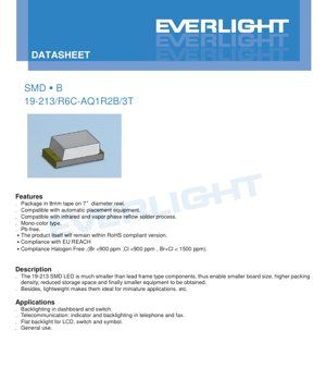
1. Product Overview
The 19-213 is a surface-mount device (SMD) LED designed for high-density electronic assemblies. Utilizing AlGaInP chip technology, it emits a brilliant red light. Its compact form factor enables significant reductions in printed circuit board (PCB) size and overall equipment dimensions, making it ideal for space-constrained applications. The component is lead-free, RoHS compliant, and adheres to EU REACH and halogen-free standards, ensuring environmental safety and regulatory acceptance.
1.1 Core Advantages
The primary advantages of this LED stem from its miniature SMD package. It offers superior compatibility with automated pick-and-place assembly lines, which streamlines high-volume manufacturing. The package is qualified for standard infrared and vapor phase reflow soldering processes. Its lightweight construction minimizes mechanical stress on PCBs and is perfectly suited for portable and miniature electronic devices.
1.2 Target Market and Applications
This LED is targeted at consumer electronics, industrial controls, and telecommunications sectors. Typical applications include backlighting for instrument panels, switches, and keypads. It is commonly used as status indicators in telephones, fax machines, and various electronic appliances. Furthermore, it serves as a flat backlight source for liquid crystal displays (LCDs) and general-purpose indicator lighting.
2. Technical Parameter Analysis
This section provides a detailed, objective interpretation of the key electrical, optical, and thermal parameters specified in the datasheet.
2.1 Absolute Maximum Ratings
The absolute maximum ratings define the stress limits beyond which permanent damage to the device may occur. These are not conditions for normal operation.
- Reverse Voltage (VR): 5V. Exceeding this voltage in reverse bias can cause junction breakdown.
- Continuous Forward Current (IF): 25mA. The maximum DC current for reliable long-term operation.
- Peak Forward Current (IFP): 60mA at a 1/10 duty cycle and 1kHz. This rating is for pulsed operation, not continuous use.
- Power Dissipation (Pd): 60mW. The maximum power the package can dissipate at an ambient temperature (Ta) of 25°C. Derating is necessary at higher temperatures.
- Electrostatic Discharge (ESD): 2000V (Human Body Model). Proper ESD handling procedures are mandatory during assembly.
- Operating & Storage Temperature: -40°C to +85°C (operating), -40°C to +90°C (storage).
- Soldering Temperature: Withstands reflow soldering with a peak temperature of 260°C for up to 10 seconds, or hand soldering at 350°C for 3 seconds per terminal.
2.2 Electro-Optical Characteristics
These parameters are measured at a forward current (IF) of 20mA and an ambient temperature of 25°C, representing typical operating conditions.
- Luminous Intensity (Iv): Ranges from a minimum of 72.0 mcd to a maximum of 180.0 mcd. The typical value is not specified, indicating performance is managed through a binning system.
- Viewing Angle (2θ1/2): Approximately 120 degrees. This wide viewing angle ensures good visibility from various perspectives.
- Peak Wavelength (λp): Typically 632 nm, placing the emission in the brilliant red portion of the spectrum.
- Dominant Wavelength (λd): Specified between 617.5 nm and 633.5 nm, with a tight tolerance of ±1nm per the note. This defines the perceived color.
- Spectral Bandwidth (Δλ): Typically 20 nm, indicating the spectral purity of the emitted red light.
- Forward Voltage (VF): Ranges from 1.75V to 2.35V at 20mA, with a tolerance of ±0.1V. This parameter is critical for current-limiting resistor calculation.
- Reverse Current (IR): Maximum of 10 µA at VR=5V. The datasheet explicitly states the device is not designed for reverse operation.
3. Binning System Explanation
To ensure color and brightness consistency in production, the LEDs are sorted into bins based on key parameters.
3.1 Luminous Intensity Binning
LEDs are categorized into four bins (Q1, Q2, R1, R2) based on their measured luminous intensity at 20mA. This allows designers to select a brightness grade suitable for their application, from standard brightness (Q1: 72-90 mcd) to high brightness (R2: 140-180 mcd).
3.2 Dominant Wavelength Binning
The dominant wavelength, which defines the precise shade of red, is binned into four codes (E4, E5, E6, E7). This binning, with a range from 617.5 nm to 633.5 nm, enables precise color matching across multiple LEDs in an array or display.
3.3 Forward Voltage Binning
Forward voltage is sorted into three bins (0, 1, 2), covering the range from 1.75V to 2.35V. Knowledge of the VF bin can help optimize the design of the current-limiting circuit for efficiency and thermal management.
4. Performance Curve Analysis
While the PDF mentions typical electro-optical characteristic curves, specific graphs for IV (Current-Voltage), temperature dependence of luminous intensity, and spectral distribution are not provided in the extracted text. In a complete analysis, these curves would be essential. The IV curve would show the exponential relationship between voltage and current. The temperature characteristic curve would typically show a decrease in luminous intensity as junction temperature rises. The spectral distribution plot would visualize the 20nm bandwidth around the 632nm peak, confirming the color purity.
5. Mechanical and Package Information
5.1 Package Dimensions
The LED has a very compact footprint. The package dimensions are 2.0mm in length, 1.25mm in width, and 0.8mm in height (typical SMD 0805 size equivalent). The cathode is typically identified by a marking or a chamfered corner on the package. The dimensional drawing provides precise measurements for land pattern design, with standard tolerances of ±0.1mm unless otherwise noted.
5.2 Polarity Identification and Solder Pad Design
Correct polarity is crucial for operation. The datasheet's package diagram indicates the anode and cathode terminals. The recommended solder pad layout ensures proper solder joint formation during reflow and provides adequate mechanical strength. Designers must adhere to these guidelines to prevent tombstoning or poor electrical connection.
6. Soldering and Assembly Guidelines
6.1 Reflow Soldering Profile
The component is compatible with lead-free reflow soldering. The recommended temperature profile includes: a pre-heating stage between 150-200°C for 60-120 seconds; a time above liquidus (217°C) of 60-150 seconds; a peak temperature not exceeding 260°C, held for a maximum of 10 seconds; and controlled heating and cooling rates (max 6°C/sec and 3°C/sec, respectively). Reflow should not be performed more than twice.
6.2 Hand Soldering Precautions
If hand soldering is necessary, extreme care must be taken. The soldering iron tip temperature should be below 350°C, and contact time per terminal should not exceed 3 seconds. A low-power iron (under 25W) is recommended. A cooling interval of at least 2 seconds should be observed between soldering each terminal to prevent thermal shock.
6.3 Storage and Moisture Sensitivity
The LEDs are packaged in a moisture-resistant barrier bag with desiccant. The bag must not be opened until the components are ready for use. After opening, unused LEDs should be stored at ≤ 30°C and ≤ 60% Relative Humidity. The "floor life" after bag opening is 168 hours (7 days). If this time is exceeded or the desiccant indicates moisture ingress, a baking treatment at 60 ± 5°C for 24 hours is required before use.
7. Packaging and Ordering Information
7.1 Packaging Specification
The LEDs are supplied on 8mm wide embossed carrier tape, wound onto 7-inch diameter reels. Each reel contains 3000 pieces. The reel and tape dimensions are provided for automated feeder setup.
7.2 Label Explanation and Model Number
The reel label contains critical information for traceability and correct application: Customer Product Number (CPN), Product Number (P/N), Packing Quantity (QTY), and the specific bin codes for Luminous Intensity Rank (CAT), Dominant Wavelength Rank (HUE), and Forward Voltage Rank (REF). The full part number 19-213/R6C-AQ1R2B/3T encodes the base product and its specific bin selections.
8. Application Design Considerations
8.1 Current Limiting and Protection
A fundamental design rule is the mandatory use of a series current-limiting resistor. The forward voltage has a range (1.75-2.35V), and the V-I characteristic is exponential. A small increase in supply voltage can cause a large, potentially destructive increase in forward current. The resistor value must be calculated based on the maximum supply voltage and the minimum forward voltage from the bin to ensure the current never exceeds the 25mA absolute maximum rating under all conditions.
8.2 Thermal Management
Although a small device, power dissipation (up to 60mW) must be considered, especially in high ambient temperatures or enclosed spaces. The PCB layout should provide adequate copper area around the solder pads to act as a heat sink, helping to conduct heat away from the LED junction and maintain performance and longevity.
8.3 Application Restrictions
The datasheet includes a critical note regarding application restrictions. This product, as specified, may not be suitable for high-reliability applications with zero-failure tolerances, such as military/aerospace systems, automotive safety-critical systems (e.g., airbags, braking), or life-support medical equipment. For such uses, products with different qualifications and testing are required.
9. Technical Comparison and Differentiation
Compared to traditional through-hole LEDs, this SMD type offers a drastic reduction in size and weight, enabling modern miniaturized electronics. Within the SMD red LED category, its key differentiators are its specific brilliant red color (AlGaInP chip), wide 120-degree viewing angle, and clearly defined binning structure for brightness and color consistency. The comprehensive handling and soldering guidelines also provide designers with clear implementation instructions, reducing risk in the assembly process.
10. Frequently Asked Questions (FAQ)
10.1 How do I calculate the series resistor?
Use Ohm's Law: R = (V_supply - VF_LED) / I_desired. Use the minimum VF from the datasheet or your specific bin (e.g., 1.75V from Bin 0) and your desired operating current (e.g., 20mA). For a 5V supply: R = (5V - 1.75V) / 0.020A = 162.5Ω. Choose the next higher standard value (e.g., 180Ω) and calculate the actual current to ensure it's below 25mA.
10.2 Can I use this for automotive interior lighting?
For non-critical interior lighting like dashboard backlighting or switch illumination, it may be suitable. However, for exterior lighting or safety-critical signals, the application restrictions note advises consulting the manufacturer for a product qualified for automotive use.
10.3 Why is the storage condition after bag opening so important?
SMD packages can absorb moisture from the atmosphere. During the high-temperature reflow soldering process, this trapped moisture can rapidly expand, causing internal delamination or "popcorning," which cracks the package and destroys the device. The 7-day floor life and baking instructions are critical to prevent this failure mode.
11. Practical Design and Usage Case
Case: Designing a Status Indicator Panel: A designer is creating a control panel with multiple red status indicators. To ensure uniform appearance, they specify LEDs from the same Dominant Wavelength bin (e.g., all E6: 625.5-629.5nm). To guarantee sufficient brightness under high ambient light, they select the R1 luminous intensity bin (112-140 mcd). They design the PCB with a 5V rail, calculate the current-limiting resistor using the maximum VF for their bin to ensure minimum brightness is met, and provide generous copper pours for thermal dissipation. They instruct manufacturing to follow the reflow profile exactly and to bake the components if the moisture barrier bag is opened more than 7 days before assembly.
12. Operating Principle
This LED is based on an Aluminum Gallium Indium Phosphide (AlGaInP) semiconductor chip. When a forward voltage exceeding the junction's threshold is applied, electrons and holes are injected into the active region where they recombine. This recombination process releases energy in the form of photons (light). The specific composition of the AlGaInP layers determines the bandgap energy, which directly corresponds to the wavelength of the emitted light—in this case, brilliant red at approximately 632 nm. The epoxy resin lens is water-clear to maximize light extraction and shape the 120-degree viewing angle.
13. Technology Trends
The trend in indicator LEDs continues toward higher efficiency (more light output per unit of electrical power), smaller package sizes for increased density, and improved color consistency through tighter binning. There is also a growing emphasis on reliability and qualification for harsh environments, including higher temperature tolerance and resistance to thermal cycling. Furthermore, integration with intelligent drivers for dimming and color control is becoming more common in advanced applications beyond simple indicators.
LED Specification Terminology
Complete explanation of LED technical terms
Photoelectric Performance
| Term | Unit/Representation | Simple Explanation | Why Important |
|---|---|---|---|
| Luminous Efficacy | lm/W (lumens per watt) | Light output per watt of electricity, higher means more energy efficient. | Directly determines energy efficiency grade and electricity cost. |
| Luminous Flux | lm (lumens) | Total light emitted by source, commonly called "brightness". | Determines if the light is bright enough. |
| Viewing Angle | ° (degrees), e.g., 120° | Angle where light intensity drops to half, determines beam width. | Affects illumination range and uniformity. |
| CCT (Color Temperature) | K (Kelvin), e.g., 2700K/6500K | Warmth/coolness of light, lower values yellowish/warm, higher whitish/cool. | Determines lighting atmosphere and suitable scenarios. |
| CRI / Ra | Unitless, 0–100 | Ability to render object colors accurately, Ra≥80 is good. | Affects color authenticity, used in high-demand places like malls, museums. |
| SDCM | MacAdam ellipse steps, e.g., "5-step" | Color consistency metric, smaller steps mean more consistent color. | Ensures uniform color across same batch of LEDs. |
| Dominant Wavelength | nm (nanometers), e.g., 620nm (red) | Wavelength corresponding to color of colored LEDs. | Determines hue of red, yellow, green monochrome LEDs. |
| Spectral Distribution | Wavelength vs intensity curve | Shows intensity distribution across wavelengths. | Affects color rendering and quality. |
Electrical Parameters
| Term | Symbol | Simple Explanation | Design Considerations |
|---|---|---|---|
| Forward Voltage | Vf | Minimum voltage to turn on LED, like "starting threshold". | Driver voltage must be ≥Vf, voltages add up for series LEDs. |
| Forward Current | If | Current value for normal LED operation. | Usually constant current drive, current determines brightness & lifespan. |
| Max Pulse Current | Ifp | Peak current tolerable for short periods, used for dimming or flashing. | Pulse width & duty cycle must be strictly controlled to avoid damage. |
| Reverse Voltage | Vr | Max reverse voltage LED can withstand, beyond may cause breakdown. | Circuit must prevent reverse connection or voltage spikes. |
| Thermal Resistance | Rth (°C/W) | Resistance to heat transfer from chip to solder, lower is better. | High thermal resistance requires stronger heat dissipation. |
| ESD Immunity | V (HBM), e.g., 1000V | Ability to withstand electrostatic discharge, higher means less vulnerable. | Anti-static measures needed in production, especially for sensitive LEDs. |
Thermal Management & Reliability
| Term | Key Metric | Simple Explanation | Impact |
|---|---|---|---|
| Junction Temperature | Tj (°C) | Actual operating temperature inside LED chip. | Every 10°C reduction may double lifespan; too high causes light decay, color shift. |
| Lumen Depreciation | L70 / L80 (hours) | Time for brightness to drop to 70% or 80% of initial. | Directly defines LED "service life". |
| Lumen Maintenance | % (e.g., 70%) | Percentage of brightness retained after time. | Indicates brightness retention over long-term use. |
| Color Shift | Δu′v′ or MacAdam ellipse | Degree of color change during use. | Affects color consistency in lighting scenes. |
| Thermal Aging | Material degradation | Deterioration due to long-term high temperature. | May cause brightness drop, color change, or open-circuit failure. |
Packaging & Materials
| Term | Common Types | Simple Explanation | Features & Applications |
|---|---|---|---|
| Package Type | EMC, PPA, Ceramic | Housing material protecting chip, providing optical/thermal interface. | EMC: good heat resistance, low cost; Ceramic: better heat dissipation, longer life. |
| Chip Structure | Front, Flip Chip | Chip electrode arrangement. | Flip chip: better heat dissipation, higher efficacy, for high-power. |
| Phosphor Coating | YAG, Silicate, Nitride | Covers blue chip, converts some to yellow/red, mixes to white. | Different phosphors affect efficacy, CCT, and CRI. |
| Lens/Optics | Flat, Microlens, TIR | Optical structure on surface controlling light distribution. | Determines viewing angle and light distribution curve. |
Quality Control & Binning
| Term | Binning Content | Simple Explanation | Purpose |
|---|---|---|---|
| Luminous Flux Bin | Code e.g., 2G, 2H | Grouped by brightness, each group has min/max lumen values. | Ensures uniform brightness in same batch. |
| Voltage Bin | Code e.g., 6W, 6X | Grouped by forward voltage range. | Facilitates driver matching, improves system efficiency. |
| Color Bin | 5-step MacAdam ellipse | Grouped by color coordinates, ensuring tight range. | Guarantees color consistency, avoids uneven color within fixture. |
| CCT Bin | 2700K, 3000K etc. | Grouped by CCT, each has corresponding coordinate range. | Meets different scene CCT requirements. |
Testing & Certification
| Term | Standard/Test | Simple Explanation | Significance |
|---|---|---|---|
| LM-80 | Lumen maintenance test | Long-term lighting at constant temperature, recording brightness decay. | Used to estimate LED life (with TM-21). |
| TM-21 | Life estimation standard | Estimates life under actual conditions based on LM-80 data. | Provides scientific life prediction. |
| IESNA | Illuminating Engineering Society | Covers optical, electrical, thermal test methods. | Industry-recognized test basis. |
| RoHS / REACH | Environmental certification | Ensures no harmful substances (lead, mercury). | Market access requirement internationally. |
| ENERGY STAR / DLC | Energy efficiency certification | Energy efficiency and performance certification for lighting. | Used in government procurement, subsidy programs, enhances competitiveness. |