1. Product Overview
The 19-21/R6C-FP1Q2L/3T is a surface-mount device (SMD) LED designed for modern, compact electronic applications. This component utilizes an AIGaInP (Aluminum Gallium Indium Phosphide) semiconductor chip to produce a brilliant red light output. Its primary advantage lies in its miniature footprint, which enables significant reductions in printed circuit board (PCB) size and allows for higher component packing density compared to traditional lead-frame type LEDs. This contributes to smaller overall equipment size and reduced storage requirements. The device is lightweight, making it particularly suitable for applications where space and weight are critical constraints.
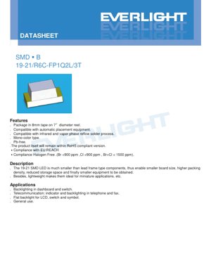
The LED is supplied in industry-standard 8mm tape on 7-inch diameter reels, ensuring compatibility with high-speed automated pick-and-place assembly equipment. It is designed for use with standard infrared (IR) and vapor phase reflow soldering processes, facilitating efficient mass production. The product is manufactured as a Pb-free (lead-free) component and complies with the European Union's RoHS (Restriction of Hazardous Substances) and REACH (Registration, Evaluation, Authorisation and Restriction of Chemicals) regulations. It is also classified as halogen-free, with bromine (Br) and chlorine (Cl) content each below 900 ppm and their combined total below 1500 ppm.
2. Technical Specifications Deep Dive
2.1 Absolute Maximum Ratings
The absolute maximum ratings define the limits beyond which permanent damage to the device may occur. These ratings are specified at an ambient temperature (Ta) of 25°C. The maximum reverse voltage (VR) is 5V. The continuous forward current (IF) should not exceed 25 mA. For pulsed operation, a peak forward current (IFP) of 60 mA is permissible under a duty cycle of 1/10 at 1 kHz. The maximum power dissipation (Pd) is 60 mW. The device can withstand an electrostatic discharge (ESD) of 2000V according to the Human Body Model (HBM). The operating temperature range (Topr) is from -40°C to +85°C, while the storage temperature range (Tstg) is slightly wider, from -40°C to +90°C. For soldering, the device can endure reflow soldering at a peak temperature of 260°C for up to 10 seconds, or hand soldering at 350°C for up to 3 seconds per terminal.
2.2 Electro-Optical Characteristics
The electro-optical characteristics are the core performance parameters, measured at Ta=25°C and a forward current (IF) of 20 mA, unless otherwise stated.
- Luminous Intensity (Iv): Ranges from a minimum of 45 millicandelas (mcd) to a maximum of 112 mcd. The typical value falls within this range, which is further divided into specific bins (P1, P2, Q1, Q2).
- Viewing Angle (2θ1/2): The half-intensity angle is typically 100 degrees, indicating a wide viewing cone.
- Peak Wavelength (λp): The wavelength at which the emitted light intensity is maximum is typically 632 nanometers (nm).
- Dominant Wavelength (λd): This is the single wavelength perceived by the human eye, ranging from 621 nm to 631 nm, categorized into bins FF1 and FF2.
- Spectral Bandwidth (Δλ): The width of the emitted spectrum at half maximum intensity is typically 20 nm.
- Forward Voltage (VF): The voltage drop across the LED when conducting 20 mA ranges from 1.7V to 2.3V, with specific bins (L19 to L24) defining narrower ranges.
- Reverse Current (IR): The leakage current when a reverse voltage of 5V is applied is 10 µA maximum.
Important notes specify tolerances: Luminous Intensity (±11%), Dominant Wavelength (±1 nm), and Forward Voltage (±0.05V). It is crucial to understand that the 5V reverse voltage rating is for IR testing only; the LED is not designed for operation under reverse bias.
3. Binning System Explanation
To ensure consistency in application design, the LEDs are sorted (binned) according to three key parameters: Luminous Intensity, Dominant Wavelength, and Forward Voltage. The product code (e.g., R6C-FP1Q2L/3T) reflects specific bins.
3.1 Luminous Intensity Binning
LEDs are categorized into four intensity bins:
- P1: 45 – 57 mcd
- P2: 57 – 72 mcd
- Q1: 72 – 90 mcd
- Q2: 90 – 112 mcd
3.2 Dominant Wavelength Binning
Color consistency is controlled through wavelength bins:
- FF1: 621 – 626 nm
- FF2: 626 – 631 nm
3.3 Forward Voltage Binning
To aid in circuit design, especially for current-limiting resistor calculation, LEDs are binned by forward voltage (VF) at 20 mA:
- L19: 1.7 – 1.8 V
- L20: 1.8 – 1.9 V
- L21: 1.9 – 2.0 V
- L22: 2.0 – 2.1 V
- L23: 2.1 – 2.2 V
- L24: 2.2 – 2.3 V
4. Performance Curve Analysis
While specific graphical curves are not detailed in the provided text, typical electro-optical characteristic curves for such an LED would include:
- Forward Current vs. Forward Voltage (I-V Curve): This non-linear curve shows the exponential relationship between current and voltage. The specified VF range at 20mA is a single point on this curve. Designers use this to determine the necessary drive voltage and to calculate the appropriate series resistor.
- Luminous Intensity vs. Forward Current (I-L Curve): This curve demonstrates how light output increases with current. It is typically linear within the recommended operating range but will saturate at higher currents. Operating at or below the 20mA test condition ensures predictable performance.
- Luminous Intensity vs. Ambient Temperature: The light output of LEDs generally decreases as the junction temperature rises. Understanding this derating is critical for applications operating at high ambient temperatures or with significant self-heating.
- Spectral Distribution: A graph showing relative intensity across wavelengths, peaking at around 632 nm with a typical bandwidth of 20 nm, confirming the brilliant red color point.
5. Mechanical and Package Information
5.1 Package Dimensions
The 19-21 SMD LED has a very compact form factor. Key dimensions (in millimeters) include a body length of 2.0 mm, a width of 1.25 mm, and a height of 0.8 mm. The detailed dimensioned drawing specifies pad layout, component outline, and the location of the cathode identifier mark. All unspecified tolerances are ±0.1 mm. Correct pad design on the PCB, as per the datasheet, is essential for reliable soldering and mechanical stability.
5.2 Polarity Identification
The device features a cathode mark, typically a notch, a green dot, or a trimmed corner on the package. Correct orientation during assembly is vital, as applying reverse voltage can damage the LED.
6. Soldering and Assembly Guidelines
6.1 Reflow Soldering Profile
A critical requirement for SMD components is adherence to the recommended reflow profile. For this Pb-free LED:
- Pre-heating: Ramp from ambient to 150–200°C over 60-120 seconds.
- Soak/Reflow: Time above 217°C (liquidus temperature for Pb-free solder) should be 60-150 seconds. The peak temperature must not exceed 260°C, and the time above 255°C must be limited to a maximum of 30 seconds.
- Cooling: The maximum cooling rate should be 6°C per second.
6.2 Hand Soldering
If manual repair is necessary, extreme care must be taken. The soldering iron tip temperature should be below 350°C, and contact time with any single terminal must not exceed 3 seconds. A low-power iron (\u003c25W) is recommended. A double-head soldering iron is suggested for removal to evenly heat both terminals and minimize stress on the package.
6.3 Storage and Moisture Sensitivity
The LEDs are packaged in a moisture-resistant barrier bag with desiccant. Key precautions:
- Do not open the bag until ready for use.
- After opening, unused LEDs must be stored at ≤ 30°C and ≤ 60% Relative Humidity.
- The "floor life" after bag opening is 168 hours (7 days).
- If the exposure time is exceeded or the desiccant indicates saturation, a baking treatment at 60 ± 5°C for 24 hours is required before reflow soldering to prevent "popcorn" effect damage.
7. Packaging and Ordering Information
7.1 Reel and Tape Specifications
The standard packaging is 3000 pieces per reel. The carrier tape width is 8 mm, wound on a 7-inch (178 mm) diameter reel. Detailed dimensions for the reel, carrier tape pockets, and cover tape are provided to ensure compatibility with automated feeders.
7.2 Label Explanation
The reel label contains crucial information for traceability and verification:
- P/N: Product Number (e.g., 19-21/R6C-FP1Q2L/3T).
- CAT: Luminous Intensity Rank (e.g., Q2).
- HUE: Chromaticity Coordinates & Dominant Wavelength Rank (e.g., FP1).
- REF: Forward Voltage Rank (e.g., L21).
- LOT No: Manufacturing Lot Number for traceability.
8. Application Recommendations
8.1 Typical Applications
The 19-21 SMD LED is versatile and suitable for various low-power indicator and backlighting roles:
- Backlighting: Illumination for dashboard instruments, membrane switches, and control panels.
- Telecommunications: Status indicators and keypad backlighting in telephones and fax machines.
- Display Technology: Flat backlighting for small liquid crystal displays (LCDs) and illuminated symbols.
- General Purpose Indication: Power status, mode indicators, and signal lights in consumer and industrial electronics.
8.2 Critical Design Considerations
- Current Limiting: An external current-limiting resistor is absolutely mandatory. The forward voltage has a range and a negative temperature coefficient. A slight increase in supply voltage or a drop in VF due to heating can cause a large, potentially destructive, increase in forward current. The resistor value must be calculated based on the power supply voltage and the maximum forward voltage (VF max) from the bin to ensure current never exceeds 25 mA under worst-case conditions.
- Thermal Management: Although power dissipation is low, ensuring adequate PCB copper area or thermal vias under the LED pads can help dissipate heat, maintaining light output stability and longevity, especially in high ambient temperature environments.
- ESD Protection: While rated for 2000V HBM, standard ESD handling precautions should be observed during assembly and handling.
9. Technical Comparison and Differentiation
The primary advantages of this 19-21 SMD LED compared to older through-hole LEDs or larger SMD packages are its miniaturization and suitability for automated assembly. The AIGaInP chip technology offers high efficiency and good color saturation for red light. Compared to some other red LED technologies, AIGaInP typically provides higher luminous intensity and better temperature stability. The comprehensive binning system allows designers to select parts with tightly controlled optical and electrical characteristics, which is crucial for applications requiring uniform appearance or precise current drive.
10. Frequently Asked Questions (FAQ)
Q: Why is a series resistor necessary?
A: LEDs are current-driven devices. Their V-I characteristic is exponential. Without a resistor to limit current, any small variation in supply voltage or LED forward voltage can lead to thermal runaway and immediate failure. The resistor sets a fixed current based on Ohm's Law.
Q: Can I drive this LED with a voltage higher than 2.3V?
A: Yes, but only if you use an appropriate series resistor to drop the excess voltage and limit the current to 20mA (or less). The driving voltage itself is not the critical parameter; the resulting current is.
Q: What does the "water clear" resin color mean?
A: The LED encapsulant (the plastic lens) is colorless and transparent. This allows the true color of the chip's emitted light (brilliant red) to pass through without any tinting or diffusion, resulting in a saturated, vivid color.
Q: How do I interpret the part number for ordering?
A: The part number 19-21/R6C-FP1Q2L/3T encodes the package style (19-21), a product code (R6C), and the specific bins for wavelength (FP1), luminous intensity (Q2), and forward voltage (L, with a subsequent number). Always refer to the full datasheet and binning tables to confirm the exact specifications of the ordered part.
11. Practical Design and Usage Case
Scenario: Designing a status indicator for a 5V USB-powered device.
1. Parameter Selection: Choose the required brightness (bin Q2 for high visibility) and color consistency (bin FF1 or FF2).
2. Circuit Design: Assuming a 5V supply (Vcc) and using the worst-case VF min (e.g., 1.7V from bin L19) to ensure current never exceeds 25mA even if VF is low. Target current (I_F) = 20 mA.
Required Resistor R = (Vcc - VF) / I_F = (5V - 1.7V) / 0.020A = 165 Ohms.
The nearest standard value is 160 Ohms or 180 Ohms. Using 180 Ohms gives I_F = (5-1.7)/180 ≈ 18.3 mA, which is safe and within spec.
Power in resistor P_R = I_F^2 * R = (0.0183)^2 * 180 ≈ 0.06W. A standard 1/8W or 1/4W resistor is sufficient.
3. PCB Layout: Place the LED and its current-limiting resistor close together. Follow the recommended pad geometry from the datasheet's dimension drawing.
4. Assembly: Follow the moisture handling and reflow soldering profile guidelines precisely.
12. Operating Principle
This LED operates on the principle of electroluminescence in a semiconductor p-n junction. The active region is composed of AIGaInP. When a forward bias voltage exceeding the junction's potential barrier (roughly 1.8V) is applied, electrons from the n-type region and holes from the p-type region are injected into the active region. When these charge carriers recombine, they release energy in the form of photons (light). The specific composition of the AIGaInP alloy determines the bandgap energy, which directly corresponds to the wavelength (color) of the emitted light—in this case, brilliant red at approximately 632 nm. The clear epoxy resin encapsulant protects the chip, acts as a lens to shape the light output (achieving the 100-degree viewing angle), and provides mechanical stability.
13. Technology Trends
The development of SMD LEDs like the 19-21 follows broader trends in electronics: miniaturization, increased efficiency, and enhanced reliability. The move to Pb-free and halogen-free materials is driven by global environmental regulations (RoHS, REACH). Advancements in semiconductor epitaxy continue to improve the luminous efficacy (light output per electrical watt) and color consistency of AIGaInP and other material systems. Furthermore, packaging technology is evolving to better manage thermal performance, allowing for higher drive currents in smaller packages, and to provide more precise optical control. The standardization of packaging (like the 19-21 footprint) and tape-and-reel formats is critical for enabling cost-effective, high-volume automated manufacturing across the electronics industry.
LED Specification Terminology
Complete explanation of LED technical terms
Photoelectric Performance
| Term | Unit/Representation | Simple Explanation | Why Important |
|---|---|---|---|
| Luminous Efficacy | lm/W (lumens per watt) | Light output per watt of electricity, higher means more energy efficient. | Directly determines energy efficiency grade and electricity cost. |
| Luminous Flux | lm (lumens) | Total light emitted by source, commonly called "brightness". | Determines if the light is bright enough. |
| Viewing Angle | ° (degrees), e.g., 120° | Angle where light intensity drops to half, determines beam width. | Affects illumination range and uniformity. |
| CCT (Color Temperature) | K (Kelvin), e.g., 2700K/6500K | Warmth/coolness of light, lower values yellowish/warm, higher whitish/cool. | Determines lighting atmosphere and suitable scenarios. |
| CRI / Ra | Unitless, 0–100 | Ability to render object colors accurately, Ra≥80 is good. | Affects color authenticity, used in high-demand places like malls, museums. |
| SDCM | MacAdam ellipse steps, e.g., "5-step" | Color consistency metric, smaller steps mean more consistent color. | Ensures uniform color across same batch of LEDs. |
| Dominant Wavelength | nm (nanometers), e.g., 620nm (red) | Wavelength corresponding to color of colored LEDs. | Determines hue of red, yellow, green monochrome LEDs. |
| Spectral Distribution | Wavelength vs intensity curve | Shows intensity distribution across wavelengths. | Affects color rendering and quality. |
Electrical Parameters
| Term | Symbol | Simple Explanation | Design Considerations |
|---|---|---|---|
| Forward Voltage | Vf | Minimum voltage to turn on LED, like "starting threshold". | Driver voltage must be ≥Vf, voltages add up for series LEDs. |
| Forward Current | If | Current value for normal LED operation. | Usually constant current drive, current determines brightness & lifespan. |
| Max Pulse Current | Ifp | Peak current tolerable for short periods, used for dimming or flashing. | Pulse width & duty cycle must be strictly controlled to avoid damage. |
| Reverse Voltage | Vr | Max reverse voltage LED can withstand, beyond may cause breakdown. | Circuit must prevent reverse connection or voltage spikes. |
| Thermal Resistance | Rth (°C/W) | Resistance to heat transfer from chip to solder, lower is better. | High thermal resistance requires stronger heat dissipation. |
| ESD Immunity | V (HBM), e.g., 1000V | Ability to withstand electrostatic discharge, higher means less vulnerable. | Anti-static measures needed in production, especially for sensitive LEDs. |
Thermal Management & Reliability
| Term | Key Metric | Simple Explanation | Impact |
|---|---|---|---|
| Junction Temperature | Tj (°C) | Actual operating temperature inside LED chip. | Every 10°C reduction may double lifespan; too high causes light decay, color shift. |
| Lumen Depreciation | L70 / L80 (hours) | Time for brightness to drop to 70% or 80% of initial. | Directly defines LED "service life". |
| Lumen Maintenance | % (e.g., 70%) | Percentage of brightness retained after time. | Indicates brightness retention over long-term use. |
| Color Shift | Δu′v′ or MacAdam ellipse | Degree of color change during use. | Affects color consistency in lighting scenes. |
| Thermal Aging | Material degradation | Deterioration due to long-term high temperature. | May cause brightness drop, color change, or open-circuit failure. |
Packaging & Materials
| Term | Common Types | Simple Explanation | Features & Applications |
|---|---|---|---|
| Package Type | EMC, PPA, Ceramic | Housing material protecting chip, providing optical/thermal interface. | EMC: good heat resistance, low cost; Ceramic: better heat dissipation, longer life. |
| Chip Structure | Front, Flip Chip | Chip electrode arrangement. | Flip chip: better heat dissipation, higher efficacy, for high-power. |
| Phosphor Coating | YAG, Silicate, Nitride | Covers blue chip, converts some to yellow/red, mixes to white. | Different phosphors affect efficacy, CCT, and CRI. |
| Lens/Optics | Flat, Microlens, TIR | Optical structure on surface controlling light distribution. | Determines viewing angle and light distribution curve. |
Quality Control & Binning
| Term | Binning Content | Simple Explanation | Purpose |
|---|---|---|---|
| Luminous Flux Bin | Code e.g., 2G, 2H | Grouped by brightness, each group has min/max lumen values. | Ensures uniform brightness in same batch. |
| Voltage Bin | Code e.g., 6W, 6X | Grouped by forward voltage range. | Facilitates driver matching, improves system efficiency. |
| Color Bin | 5-step MacAdam ellipse | Grouped by color coordinates, ensuring tight range. | Guarantees color consistency, avoids uneven color within fixture. |
| CCT Bin | 2700K, 3000K etc. | Grouped by CCT, each has corresponding coordinate range. | Meets different scene CCT requirements. |
Testing & Certification
| Term | Standard/Test | Simple Explanation | Significance |
|---|---|---|---|
| LM-80 | Lumen maintenance test | Long-term lighting at constant temperature, recording brightness decay. | Used to estimate LED life (with TM-21). |
| TM-21 | Life estimation standard | Estimates life under actual conditions based on LM-80 data. | Provides scientific life prediction. |
| IESNA | Illuminating Engineering Society | Covers optical, electrical, thermal test methods. | Industry-recognized test basis. |
| RoHS / REACH | Environmental certification | Ensures no harmful substances (lead, mercury). | Market access requirement internationally. |
| ENERGY STAR / DLC | Energy efficiency certification | Energy efficiency and performance certification for lighting. | Used in government procurement, subsidy programs, enhances competitiveness. |