Table of Contents
- 1. Product Overview
- 2. Technical Specifications Deep Dive
- 2.1 Absolute Maximum Ratings
- 2.2 Electro-Optical Characteristics
- 3. Binning System Explanation
- 3.1 Luminous Intensity Binning
- 3.2 Dominant Wavelength Binning
- 3.3 Forward Voltage Binning
- 4. Performance Curve Analysis
- 4.1 Luminous Intensity vs. Forward Current
- 4.2 Luminous Intensity vs. Ambient Temperature
- 4.3 Forward Current Derating Curve
- 4.4 Spectrum Distribution
- 4.5 Forward Voltage vs. Forward Current
- 4.6 Radiation Diagram
- 5. Mechanical and Package Information
- 5.1 Package Dimensions
- 5.2 Polarity Identification
- 6. Soldering and Assembly Guidelines
- 6.1 Over-Current Protection
- 6.2 Storage and Moisture Sensitivity
- 6.3 Reflow Soldering Profile
- 6.4 Hand Soldering and Repair
- 7. Packaging and Ordering Information
- 7.1 Reel and Tape Specifications
- 7.2 Label Explanation
- 8. Application Suggestions
- 8.1 Typical Application Scenarios
- 8.2 Design Considerations
- 9. Technical Comparison and Differentiation
- 10. Frequently Asked Questions (Based on Technical Parameters)
- 10.1 What resistor value should I use with a 5V supply?
- 10.2 Can I drive this LED at 30mA for more brightness?
- 10.3 Why is there a 7-day limit after opening the moisture barrier bag?
- 10.4 What does the bin code "R6C-AP1Q2L/3T" in the part number signify?
- 11. Practical Design and Usage Case
- 12. Technology Principle Introduction
- 13. Industry Trends and Developments
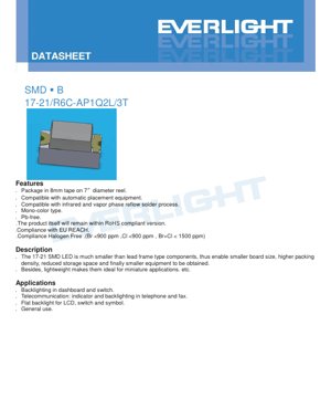
1. Product Overview
The 17-21/R6C-AP1Q2L/3T is a surface-mount device (SMD) LED utilizing AIGaInP semiconductor technology to produce a Brilliant Red light output. This component is designed for high-density PCB applications where space and weight are critical constraints. Its primary advantages include a significantly reduced footprint compared to lead-frame type LEDs, enabling more compact board designs, higher packing density, and ultimately smaller end-user equipment. The lightweight construction makes it particularly suitable for miniature and portable electronic devices.
The LED is packaged on 8mm tape wound onto a 7-inch diameter reel, making it fully compatible with standard automated pick-and-place assembly equipment. It is formulated to be Pb-free and compliant with major environmental regulations including RoHS, EU REACH, and halogen-free standards (Br <900 ppm, Cl <900 ppm, Br+Cl < 1500 ppm). The device is compatible with both infrared and vapor phase reflow soldering processes.
2. Technical Specifications Deep Dive
2.1 Absolute Maximum Ratings
The device is rated for operation under the following absolute maximum conditions, beyond which permanent damage may occur. All ratings are specified at an ambient temperature (Ta) of 25°C.
- Reverse Voltage (VR): 5 V. Exceeding this voltage in reverse bias can cause junction breakdown.
- Continuous Forward Current (IF): 25 mA. This is the maximum DC current for reliable operation.
- Peak Forward Current (IFP): 60 mA. This rating applies under pulsed conditions with a duty cycle of 1/10 at 1 kHz.
- Power Dissipation (Pd): 60 mW. This is the maximum power the package can dissipate.
- Electrostatic Discharge (ESD) Human Body Model (HBM): 2000 V. Proper ESD handling procedures are required during assembly.
- Operating Temperature Range (Topr): -40°C to +85°C.
- Storage Temperature Range (Tstg): -40°C to +90°C.
- Soldering Temperature (Tsol): The device can withstand reflow soldering with a peak temperature of 260°C for 10 seconds, or hand soldering at 350°C for 3 seconds per terminal.
2.2 Electro-Optical Characteristics
The key performance parameters are measured at Ta=25°C and a standard test current of IF=20 mA. These define the core light output and electrical behavior of the LED.
- Luminous Intensity (Iv): Ranges from a minimum of 45.0 mcd to a maximum of 112.0 mcd. The typical value falls within this range based on the specific bin code.
- Viewing Angle (2θ1/2): A typical wide viewing angle of 140 degrees, providing broad, even illumination.
- Peak Wavelength (λp): Typically 632 nm, indicating the wavelength at which the spectral power distribution is highest.
- Dominant Wavelength (λd): Ranges from 617.5 nm to 633.5 nm. This is the single-wavelength perception of the LED's color by the human eye and is a critical parameter for color consistency.
- Spectral Bandwidth (Δλ): Typically 20 nm, defining the spectral purity of the emitted red light.
- Forward Voltage (VF): Ranges from 1.7 V to 2.3 V at IF=20mA. This parameter is crucial for circuit design and current-limiting resistor calculation.
- Reverse Current (IR): Maximum of 10 μA when a reverse voltage of 5V is applied. The device is not designed for operation in reverse bias.
Important Notes: Tolerances are specified as ±11% for Luminous Intensity, ±1nm for Dominant Wavelength, and ±0.05V for Forward Voltage. The reverse voltage condition is for IR testing only; the LED should not be operated in reverse bias.
3. Binning System Explanation
To ensure consistent performance in production, LEDs are sorted into bins based on key parameters. This allows designers to select parts that meet specific application requirements for brightness and color.
3.1 Luminous Intensity Binning
Binned at IF=20mA. The bin code (e.g., P1, Q2) defines the minimum and maximum luminous intensity.
- P1: 45.0 - 57.0 mcd
- P2: 57.0 - 72.0 mcd
- Q1: 72.0 - 90.0 mcd
- Q2: 90.0 - 112.0 mcd
3.2 Dominant Wavelength Binning
Binned at IF=20mA. The bin code (E4-E7) defines the color point of the red emission.
- E4: 617.5 - 621.5 nm
- E5: 621.5 - 625.5 nm
- E6: 625.5 - 629.5 nm
- E7: 629.5 - 633.5 nm
3.3 Forward Voltage Binning
Binned at IF=20mA. The bin code (19-24) defines the electrical characteristics for power supply design.
- 19: 1.7 - 1.8 V
- 20: 1.8 - 1.9 V
- 21: 1.9 - 2.0 V
- 22: 2.0 - 2.1 V
- 23: 2.1 - 2.2 V
- 24: 2.2 - 2.3 V
4. Performance Curve Analysis
The datasheet provides several characteristic curves that illustrate the device's behavior under varying conditions. These are essential for robust system design.
4.1 Luminous Intensity vs. Forward Current
This curve shows a generally linear relationship between forward current (IF) and relative luminous intensity up to the maximum rated current. It confirms that light output is directly proportional to drive current within the operating range.
4.2 Luminous Intensity vs. Ambient Temperature
The curve demonstrates the temperature dependence of light output. Luminous intensity typically decreases as the ambient temperature (Ta) increases, especially above room temperature. This derating must be accounted for in applications with high ambient temperatures or poor thermal management.
4.3 Forward Current Derating Curve
This graph defines the maximum allowable continuous forward current as a function of ambient temperature. As temperature rises, the maximum permissible current must be reduced to stay within the device's power dissipation limits, preventing thermal runaway and ensuring long-term reliability.
4.4 Spectrum Distribution
The spectral output curve shows a narrow, single peak centered around 632 nm, characteristic of AIGaInP-based red LEDs. The typical 20 nm bandwidth indicates good color saturation.
4.5 Forward Voltage vs. Forward Current
This IV curve shows the exponential relationship typical of a diode. The forward voltage increases with current, and its value at 20mA is the key parameter used for binning and circuit design.
4.6 Radiation Diagram
The polar plot illustrates the spatial distribution of light intensity, confirming the wide 140-degree viewing angle. The intensity is highest at 0 degrees (perpendicular to the LED face) and decreases towards the edges.
5. Mechanical and Package Information
5.1 Package Dimensions
The 17-21 SMD LED has a compact rectangular package. Key dimensions (in mm, tolerance ±0.1mm unless specified) include a body length of 1.6 mm, a width of 0.8 mm, and a height of 0.6 mm. The datasheet provides a detailed drawing showing all critical dimensions, including pad spacing and solder land recommendations.
5.2 Polarity Identification
The cathode is clearly marked on the package. Correct polarity orientation is essential during PCB layout and assembly to ensure proper operation. The datasheet diagram indicates the location of this marking relative to the package geometry.
6. Soldering and Assembly Guidelines
6.1 Over-Current Protection
An external current-limiting resistor is mandatory. The forward voltage has a negative temperature coefficient, meaning that as the junction heats up, VF drops, which can lead to a rapid increase in current if driven by a constant voltage source. This can cause thermal runaway and device failure. A series resistor provides a linear, stable current drive.
6.2 Storage and Moisture Sensitivity
The LEDs are packaged in a moisture-resistant barrier bag with desiccant to prevent moisture absorption, which can cause "popcorning" (package cracking) during reflow soldering.
- Do not open the bag until ready for use.
- After opening, use within 168 hours (7 days) if stored at ≤30°C and ≤60% RH.
- If not used within this period, or if the desiccant indicator shows saturation, the components must be baked at 60 ±5°C for 24 hours before use.
6.3 Reflow Soldering Profile
A Pb-free reflow profile is specified:
- Pre-heating: 150-200°C for 60-120 seconds.
- Time Above Liquidus (TAL): 60-150 seconds above 217°C.
- Peak Temperature: Maximum of 260°C, held for a maximum of 10 seconds.
- Heating Rate: Maximum 6°C/sec up to 255°C, then maximum 3°C/sec to peak.
- Reflow soldering should not be performed more than two times.
- Avoid mechanical stress on the package during heating and cooling.
6.4 Hand Soldering and Repair
If hand soldering is necessary, use a soldering iron with a tip temperature <350°C, apply heat to each terminal for <3 seconds, and use an iron with a capacity of <25W. Allow a minimum 2-second interval between soldering each terminal. Repair after initial soldering is strongly discouraged. If absolutely unavoidable, use a dual-head soldering iron to simultaneously heat both terminals and lift the component to avoid stressing the solder joints. Always verify device functionality after any repair attempt.
7. Packaging and Ordering Information
7.1 Reel and Tape Specifications
The components are supplied in embossed carrier tape on 7-inch diameter reels. The tape width is 8 mm. Each reel contains 3000 pieces. Detailed drawings for reel dimensions, carrier tape pocket dimensions, and cover tape specifications are provided to ensure compatibility with automated assembly equipment.
7.2 Label Explanation
The reel label contains several key identifiers:
- CPN: Customer's Product Number (optional).
- P/N: Manufacturer's full part number (e.g., 17-21/R6C-AP1Q2L/3T).
- QTY: Packing quantity per reel (3000 PCS).
- CAT: Luminous Intensity bin rank (e.g., Q2).
- HUE: Chromaticity/Dominant Wavelength bin rank (e.g., E6).
- REF: Forward Voltage bin rank (e.g., 21).
- LOT No: Traceable manufacturing lot number.
8. Application Suggestions
8.1 Typical Application Scenarios
- Backlighting: Ideal for dashboard indicators, switch illumination, and symbol backlighting due to its small size and even viewing angle.
- Telecommunication Equipment: Status indicators and keypad backlighting in telephones, fax machines, and other communication devices.
- LCD Flat Backlighting: Can be used in arrays for small, low-profile LCD displays.
- General Indicator Use: Power status, mode indication, and alert signals in a wide variety of consumer and industrial electronics.
8.2 Design Considerations
- Current Drive: Always use a constant current source or a voltage source with a series resistor. Calculate the resistor value using R = (Vsupply - VF) / IF, using the maximum VF from the bin or datasheet to ensure current does not exceed 20mA (or the chosen operating point) under worst-case conditions.
- Thermal Management: While the package is small, ensure adequate PCB copper area or thermal vias if operating at high ambient temperatures or near maximum current to maintain junction temperature within limits.
- Optical Design: The wide 140-degree viewing angle provides broad illumination. For focused light, external lenses or light guides may be required.
- ESD Protection: Implement standard ESD precautions during handling and assembly. Consider adding transient voltage suppression on the input lines if the LED is connected to user-accessible ports.
9. Technical Comparison and Differentiation
The 17-21 package offers distinct advantages in the landscape of indicator LEDs.
- vs. Leaded LEDs (e.g., 3mm, 5mm): The primary advantage is the dramatically reduced footprint and height, enabling modern, miniaturized designs. It also eliminates the need for manual insertion and cutting/bending of leads, streamlining automated assembly.
- vs. Other SMD LEDs (e.g., 0402, 0603): The 17-21 package (1.6x0.8mm) is slightly larger than the smallest chip LEDs, which can make it easier to handle and solder manually if needed, while still being very compact. It may also offer higher light output due to a potentially larger chip size within the package.
- Material Technology (AIGaInP): Compared to older technologies like GaAsP, AIGaInP provides higher efficiency, brighter output, and better color purity (saturated red) for the same input current.
10. Frequently Asked Questions (Based on Technical Parameters)
10.1 What resistor value should I use with a 5V supply?
Using the maximum VF of 2.3V (from bin 24) and a target IF of 20mA for safety: R = (5V - 2.3V) / 0.020A = 135 Ohms. The nearest standard value is 130 or 150 Ohms. The power rating of the resistor should be at least P = I^2 * R = (0.02^2)*150 = 0.06W, so a 1/8W (0.125W) resistor is sufficient.
10.2 Can I drive this LED at 30mA for more brightness?
No. The Absolute Maximum Rating for continuous forward current is 25 mA. Operating at 30 mA exceeds this rating, which will reduce reliability, accelerate lumen depreciation, and may cause immediate failure. For higher brightness, select an LED from a higher luminous intensity bin (e.g., Q2) or a product series rated for higher current.
10.3 Why is there a 7-day limit after opening the moisture barrier bag?
The plastic packaging material can absorb moisture from the air. During the high-temperature reflow soldering process, this absorbed moisture rapidly turns to steam, creating internal pressure that can delaminate the package or crack the epoxy lens ("popcorning"). The 7-day limit, under controlled humidity, ensures moisture absorption remains below a critical level.
10.4 What does the bin code "R6C-AP1Q2L/3T" in the part number signify?
While the full decoding may be proprietary, it typically encodes the product series (17-21), the color (R for Red, 6C likely specifying the specific chromaticity), and the performance bins for intensity, wavelength, and voltage (implied by Q2, etc.). The "3T" may refer to tape packaging. For exact binning, refer to the CAT, HUE, and REF codes on the reel label.
11. Practical Design and Usage Case
Scenario: Designing a multi-indicator status panel for a portable medical device.
The device requires 5 independent red status LEDs (Battery Low, Charging, Error, Mode 1, Mode 2) on a densely populated main PCB. Space is extremely limited, and the device must be lightweight.
Solution Implementation:
- Component Selection: The 17-21/R6C-AP1Q2L/3T LED is chosen for its ultra-compact 1.6x0.8mm footprint, which saves valuable board space compared to larger alternatives.
- Circuit Design: The system microcontroller operates at 3.3V. Using a typical VF of 2.0V (bin 21) and a design IF of 15mA to ensure long life and account for minor temperature variations: R = (3.3V - 2.0V) / 0.015A = 86.7 Ohms. A 82 Ohm 1% resistor is selected, resulting in a slightly higher IF of ~16mA, which is well within the 25mA limit.
- PCB Layout: LEDs are placed with a center-to-center spacing of 3.0mm, allowing clear visual separation. The cathode pad is connected to the microcontroller GPIO pin (configured as an open-drain output) to switch the LED on/off. The anode pad connects to 3.3V through the current-limiting resistor. A small keep-out area under the LED is maintained to prevent solder wicking.
- Assembly: The LEDs are supplied on 8mm tape reels, compatible with the pick-and-place machine. The Pb-free reflow profile from section 6.3 is programmed into the oven. The factory floor follows the moisture control procedures, baking a reel that had been opened for a sample check more than 7 days prior to the production run.
- Result: A reliable, bright, and consistent set of status indicators is achieved in a minimal area, contributing to the overall miniaturization and reliability of the final medical device.
12. Technology Principle Introduction
This LED is based on Aluminum Indium Gallium Phosphide (AIGaInP) semiconductor material grown on a substrate. When a forward voltage is applied across the p-n junction, electrons from the n-type region and holes from the p-type region are injected into the active region. When these charge carriers recombine, they release energy in the form of photons (light). The specific wavelength of the emitted light--in this case, brilliant red around 632 nm--is determined by the bandgap energy of the AIGaInP alloy composition. By carefully controlling the ratios of Aluminum, Indium, Gallium, and Phosphorus during crystal growth, manufacturers can tune the bandgap to produce specific colors in the red, orange, and yellow spectrum with high efficiency and color purity. The epoxy resin package serves to protect the delicate semiconductor chip, acts as a lens to shape the light output beam (resulting in the 140-degree viewing angle), and provides the mechanical structure for soldering.
13. Industry Trends and Developments
The trend in indicator and backlight LEDs continues strongly towards miniaturization, increased efficiency, and higher reliability. Packages like the 17-21 are part of this evolution, bridging the gap between the smallest chip-scale packages and larger, more traditional SMDs. There is a growing emphasis on tighter binning tolerances for both color and flux to meet the demands of applications requiring uniform appearance, such as indicator arrays and backlight panels. Furthermore, the drive for higher efficiency (more lumens per watt) is constant, pushing material science to improve internal quantum efficiency and light extraction from the package. Integration is another trend, with multi-LED packages and LEDs with built-in ICs for control or protection becoming more common, although discrete components like the 17-21 remain essential for flexible, cost-effective designs. Environmental compliance (RoHS, REACH, Halogen-Free) is now a standard requirement across the industry, as reflected in this component's specifications.
LED Specification Terminology
Complete explanation of LED technical terms
Photoelectric Performance
| Term | Unit/Representation | Simple Explanation | Why Important |
|---|---|---|---|
| Luminous Efficacy | lm/W (lumens per watt) | Light output per watt of electricity, higher means more energy efficient. | Directly determines energy efficiency grade and electricity cost. |
| Luminous Flux | lm (lumens) | Total light emitted by source, commonly called "brightness". | Determines if the light is bright enough. |
| Viewing Angle | ° (degrees), e.g., 120° | Angle where light intensity drops to half, determines beam width. | Affects illumination range and uniformity. |
| CCT (Color Temperature) | K (Kelvin), e.g., 2700K/6500K | Warmth/coolness of light, lower values yellowish/warm, higher whitish/cool. | Determines lighting atmosphere and suitable scenarios. |
| CRI / Ra | Unitless, 0–100 | Ability to render object colors accurately, Ra≥80 is good. | Affects color authenticity, used in high-demand places like malls, museums. |
| SDCM | MacAdam ellipse steps, e.g., "5-step" | Color consistency metric, smaller steps mean more consistent color. | Ensures uniform color across same batch of LEDs. |
| Dominant Wavelength | nm (nanometers), e.g., 620nm (red) | Wavelength corresponding to color of colored LEDs. | Determines hue of red, yellow, green monochrome LEDs. |
| Spectral Distribution | Wavelength vs intensity curve | Shows intensity distribution across wavelengths. | Affects color rendering and quality. |
Electrical Parameters
| Term | Symbol | Simple Explanation | Design Considerations |
|---|---|---|---|
| Forward Voltage | Vf | Minimum voltage to turn on LED, like "starting threshold". | Driver voltage must be ≥Vf, voltages add up for series LEDs. |
| Forward Current | If | Current value for normal LED operation. | Usually constant current drive, current determines brightness & lifespan. |
| Max Pulse Current | Ifp | Peak current tolerable for short periods, used for dimming or flashing. | Pulse width & duty cycle must be strictly controlled to avoid damage. |
| Reverse Voltage | Vr | Max reverse voltage LED can withstand, beyond may cause breakdown. | Circuit must prevent reverse connection or voltage spikes. |
| Thermal Resistance | Rth (°C/W) | Resistance to heat transfer from chip to solder, lower is better. | High thermal resistance requires stronger heat dissipation. |
| ESD Immunity | V (HBM), e.g., 1000V | Ability to withstand electrostatic discharge, higher means less vulnerable. | Anti-static measures needed in production, especially for sensitive LEDs. |
Thermal Management & Reliability
| Term | Key Metric | Simple Explanation | Impact |
|---|---|---|---|
| Junction Temperature | Tj (°C) | Actual operating temperature inside LED chip. | Every 10°C reduction may double lifespan; too high causes light decay, color shift. |
| Lumen Depreciation | L70 / L80 (hours) | Time for brightness to drop to 70% or 80% of initial. | Directly defines LED "service life". |
| Lumen Maintenance | % (e.g., 70%) | Percentage of brightness retained after time. | Indicates brightness retention over long-term use. |
| Color Shift | Δu′v′ or MacAdam ellipse | Degree of color change during use. | Affects color consistency in lighting scenes. |
| Thermal Aging | Material degradation | Deterioration due to long-term high temperature. | May cause brightness drop, color change, or open-circuit failure. |
Packaging & Materials
| Term | Common Types | Simple Explanation | Features & Applications |
|---|---|---|---|
| Package Type | EMC, PPA, Ceramic | Housing material protecting chip, providing optical/thermal interface. | EMC: good heat resistance, low cost; Ceramic: better heat dissipation, longer life. |
| Chip Structure | Front, Flip Chip | Chip electrode arrangement. | Flip chip: better heat dissipation, higher efficacy, for high-power. |
| Phosphor Coating | YAG, Silicate, Nitride | Covers blue chip, converts some to yellow/red, mixes to white. | Different phosphors affect efficacy, CCT, and CRI. |
| Lens/Optics | Flat, Microlens, TIR | Optical structure on surface controlling light distribution. | Determines viewing angle and light distribution curve. |
Quality Control & Binning
| Term | Binning Content | Simple Explanation | Purpose |
|---|---|---|---|
| Luminous Flux Bin | Code e.g., 2G, 2H | Grouped by brightness, each group has min/max lumen values. | Ensures uniform brightness in same batch. |
| Voltage Bin | Code e.g., 6W, 6X | Grouped by forward voltage range. | Facilitates driver matching, improves system efficiency. |
| Color Bin | 5-step MacAdam ellipse | Grouped by color coordinates, ensuring tight range. | Guarantees color consistency, avoids uneven color within fixture. |
| CCT Bin | 2700K, 3000K etc. | Grouped by CCT, each has corresponding coordinate range. | Meets different scene CCT requirements. |
Testing & Certification
| Term | Standard/Test | Simple Explanation | Significance |
|---|---|---|---|
| LM-80 | Lumen maintenance test | Long-term lighting at constant temperature, recording brightness decay. | Used to estimate LED life (with TM-21). |
| TM-21 | Life estimation standard | Estimates life under actual conditions based on LM-80 data. | Provides scientific life prediction. |
| IESNA | Illuminating Engineering Society | Covers optical, electrical, thermal test methods. | Industry-recognized test basis. |
| RoHS / REACH | Environmental certification | Ensures no harmful substances (lead, mercury). | Market access requirement internationally. |
| ENERGY STAR / DLC | Energy efficiency certification | Energy efficiency and performance certification for lighting. | Used in government procurement, subsidy programs, enhances competitiveness. |