Table of Contents
- 1. Product Overview
- 2. Technical Parameter Deep Dive
- 2.1 Absolute Maximum Ratings
- 2.2 Electro-Optical Characteristics
- 3. Binning System Explanation
- 3.1 Luminous Intensity Binning
- 3.2 Dominant Wavelength Binning
- 3.3 Forward Voltage Binning
- 4. Performance Curve Analysis
- 4.1 Forward Current vs. Forward Voltage (I-V Curve)
- 4.2 Relative Luminous Intensity vs. Ambient Temperature
- 4.3 Relative Luminous Intensity vs. Forward Current
- 4.4 Spectrum Distribution
- 4.5 Forward Current Derating Curve
- 4.6 Radiation Diagram
- 5. Mechanical and Packaging Information
- 5.1 Package Dimensions
- 5.2 Moisture Resistant Packaging and Reel Information
- 6. Soldering and Assembly Guidelines
- 6.1 Storage and Handling
- 6.2 Reflow Soldering Profile (Pb-free)
- 6.3 Hand Soldering
- 7. Application Suggestions
- 7.1 Typical Application Scenarios
- 7.2 Design Considerations and Precautions
- 8. Technical Comparison and Differentiation
- 9. Frequently Asked Questions (Based on Technical Parameters)
- 9.1 Why is a current-limiting resistor absolutely necessary?
- 9.2 Can I drive this LED with a 3.3V or 5V supply?
- 9.3 What happens if I operate the LED at its peak current (60mA) continuously?
- 9.4 How do I interpret the bin codes on the reel label?
- 9.5 Why is the storage and baking procedure so important?
- 10. Practical Design and Usage Case
- 10.1 Designing a Multi-LED Status Indicator Panel
- 11. Operating Principle Introduction
- 12. Technology Trends and Context
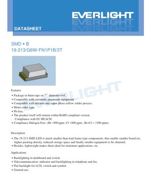
1. Product Overview
The 19-213/G6W-FN1P1B/3T is a surface-mount device (SMD) LED designed for high-density electronic assemblies. It features a compact form factor that enables smaller printed circuit board (PCB) designs, reduced storage requirements, and ultimately contributes to the miniaturization of end equipment. Its lightweight construction makes it particularly suitable for applications where space and weight are critical constraints.
This LED is a mono-color type, emitting a Brilliant Yellow Green light. It is constructed using AlGaInP (Aluminum Gallium Indium Phosphide) semiconductor material, which is known for its high efficiency in the yellow to red wavelength spectrum. The device is housed in a water-diffused resin package, which helps in achieving a wide viewing angle.
The product is compliant with key environmental and safety standards, including being Pb-free (lead-free), RoHS compliant, EU REACH compliant, and Halogen Free, with bromine (Br) and chlorine (Cl) content strictly controlled below specified limits (Br <900 ppm, Cl <900 ppm, Br+Cl < 1500 ppm).
2. Technical Parameter Deep Dive
2.1 Absolute Maximum Ratings
The Absolute Maximum Ratings define the limits beyond which permanent damage to the device may occur. These ratings are specified at an ambient temperature (Ta) of 25°C and should not be exceeded under any operating conditions.
- Reverse Voltage (VR): 5 V. Applying a voltage higher than this in the reverse direction can cause junction breakdown.
- Continuous Forward Current (IF): 25 mA. This is the maximum DC current that can be continuously passed through the LED.
- Peak Forward Current (IFP): 60 mA. This rating applies under pulsed conditions with a duty cycle of 1/10 at 1 kHz. It allows for higher instantaneous currents for short durations, such as in multiplexing circuits.
- Power Dissipation (Pd): 60 mW. This is the maximum amount of power the device can dissipate as heat. Exceeding this limit can lead to overheating and reduced lifespan.
- Operating Temperature (Topr): -40°C to +85°C. The LED is designed to function within this ambient temperature range.
- Storage Temperature (Tstg): -40°C to +90°C. The device can be stored within this range when not in operation.
- Electrostatic Discharge (ESD) Human Body Model (HBM): 2000 V. This indicates the LED's sensitivity to static electricity. Proper ESD handling procedures must be followed during assembly and handling.
- Soldering Temperature (Tsol): The device can withstand reflow soldering at 260°C for a maximum of 10 seconds or hand soldering at 350°C for a maximum of 3 seconds per terminal.
2.2 Electro-Optical Characteristics
The Electro-Optical Characteristics are measured at Ta=25°C and an IF of 20 mA, which is the typical test condition. These parameters define the light output and electrical behavior of the LED.
- Luminous Intensity (Iv): Ranges from a minimum of 28.5 mcd to a maximum of 57.0 mcd. The actual value is determined by the binning process (see Section 3). A tolerance of ±11% applies to the luminous intensity.
- Viewing Angle (2θ1/2): Typically 130 degrees. This is the full angle at which the luminous intensity is half of the intensity at 0 degrees (on-axis). The wide viewing angle is a result of the water-diffused resin, making it suitable for applications requiring broad illumination.
- Peak Wavelength (λp): Typically 575 nm. This is the wavelength at which the spectral power distribution of the emitted light is at its maximum.
- Dominant Wavelength (λd): Ranges from 570.0 nm to 574.5 nm. This is the single wavelength perceived by the human eye that best matches the color of the emitted light. It has a tolerance of ±1 nm.
- Spectrum Radiation Bandwidth (Δλ): Typically 20 nm. This parameter indicates the spectral width of the emitted light, measured at half the maximum intensity (Full Width at Half Maximum - FWHM).
- Forward Voltage (VF): Ranges from 1.75 V to 2.35 V at IF=20mA. The specific value is determined by the voltage bin (see Section 3). A tolerance of ±0.1V applies.
- Reverse Current (IR): Maximum of 10 μA when a reverse voltage (VR) of 5V is applied. It is crucial to note that this device is not designed for reverse operation; this test condition is for characterization only.
3. Binning System Explanation
To ensure consistency in color and brightness, LEDs are sorted into bins based on key parameters. This allows designers to select parts that meet specific application requirements for uniformity.
3.1 Luminous Intensity Binning
LEDs are categorized into three bins (N1, N2, P1) based on their measured luminous intensity at IF=20mA.
- Bin N1: 28.5 mcd (Min) to 36.0 mcd (Max)
- Bin N2: 36.0 mcd (Min) to 45.0 mcd (Max)
- Bin P1: 45.0 mcd (Min) to 57.0 mcd (Max)
Selecting a tighter bin (e.g., P1 only) ensures all LEDs in an array will have very similar brightness.
3.2 Dominant Wavelength Binning
LEDs are sorted into three bins (CC2, CC3, CC4) to control the precise shade of yellow-green light.
- Bin CC2: 570.0 nm (Min) to 571.5 nm (Max)
- Bin CC3: 571.5 nm (Min) to 573.0 nm (Max)
- Bin CC4: 573.0 nm (Min) to 574.5 nm (Max)
This binning is critical for applications where color consistency is paramount, such as in multi-LED indicators or backlighting units.
3.3 Forward Voltage Binning
LEDs are grouped into three voltage bins (0, 1, 2) to manage power supply design and current matching in series/parallel circuits.
- Bin 0: 1.75 V (Min) to 1.95 V (Max)
- Bin 1: 1.95 V (Min) to 2.15 V (Max)
- Bin 2: 2.15 V (Min) to 2.35 V (Max)
Using LEDs from the same voltage bin simplifies current-limiting resistor calculation and improves uniformity in driven current.
4. Performance Curve Analysis
The datasheet provides several characteristic curves that illustrate the LED's behavior under varying conditions. Understanding these is key to robust circuit design.
4.1 Forward Current vs. Forward Voltage (I-V Curve)
The I-V curve shows the exponential relationship between current and voltage. For this LED, at a typical operating current of 20 mA, the forward voltage falls between 1.75V and 2.35V depending on the bin. The curve highlights the importance of using a current-limiting device (resistor or constant current driver) rather than a constant voltage source, as a small increase in voltage can cause a large, potentially damaging increase in current.
4.2 Relative Luminous Intensity vs. Ambient Temperature
This curve demonstrates the temperature dependence of light output. Luminous intensity typically decreases as the ambient temperature rises. For example, at the maximum operating temperature of +85°C, the light output may be significantly lower than at 25°C. Designers must account for this derating in applications that operate at high ambient temperatures to ensure sufficient brightness is maintained.
4.3 Relative Luminous Intensity vs. Forward Current
This graph shows that light output increases with forward current, but the relationship is not perfectly linear, especially at higher currents. Operating above the recommended continuous current (25 mA) may yield diminishing returns in brightness while significantly increasing heat generation and accelerating lumen depreciation.
4.4 Spectrum Distribution
The spectral distribution curve confirms the monochromatic nature of the LED, with a single peak around 575 nm (yellow-green) and a typical FWHM of 20 nm. The narrow bandwidth is characteristic of AlGaInP-based LEDs.
4.5 Forward Current Derating Curve
This critical curve dictates the maximum allowable forward current as a function of ambient temperature. As temperature increases, the maximum permissible current must be reduced to stay within the device's power dissipation and thermal limits. For reliable long-term operation, the derating curve must be strictly followed.
4.6 Radiation Diagram
The radiation pattern (or spatial distribution) is typically Lambertian or near-Lambertian for a diffused package, confirming the wide 130-degree viewing angle. This pattern is ideal for applications requiring even, wide-area illumination rather than a focused beam.
5. Mechanical and Packaging Information
5.1 Package Dimensions
The LED has a compact SMD footprint. Key dimensions (in mm, tolerance ±0.1mm unless specified) include:
- Overall Length: 2.0 mm
- Overall Width: 1.25 mm
- Overall Height: 1.1 mm
- Lead (Terminal) Dimensions and spacing are provided for PCB land pattern design.
The cathode is typically identified by a marking on the package or a specific pad geometry (e.g., a notch or a green marking). Designers must consult the detailed dimension drawing to correctly identify polarity and design the solder pad layout.
5.2 Moisture Resistant Packaging and Reel Information
The LEDs are supplied in moisture-resistant packaging to prevent damage from ambient humidity, which is critical for MSL (Moisture Sensitivity Level) compliance.
- Packing: The devices are packaged on 8mm wide carrier tape, wound onto a 7-inch diameter reel.
- Quantity: 3000 pieces per reel.
- Moisture Barrier Bag: The reel is sealed inside an aluminum moisture-proof bag along with a desiccant and a humidity indicator card.
- Label Information: The reel label includes critical information such as Part Number (P/N), quantity (QTY), and the specific Binning Codes for Luminous Intensity (CAT), Dominant Wavelength (HUE), and Forward Voltage (REF).
6. Soldering and Assembly Guidelines
Proper handling and soldering are essential for reliability.
6.1 Storage and Handling
- Do not open the moisture-proof bag until ready for use.
- After opening, unused LEDs should be stored at ≤30°C and ≤60% Relative Humidity.
- The "Floor Life" after bag opening is 168 hours (7 days). If exceeded, or if the desiccant indicator shows saturation, the LEDs must be baked at 60 ±5°C for 24 hours before use.
- Always follow ESD (Electrostatic Discharge) precautions during handling.
6.2 Reflow Soldering Profile (Pb-free)
The recommended reflow profile is crucial for Pb-free (SAC) solder alloys.
- Pre-heating: 150-200°C for 60-120 seconds.
- Time Above Liquidus (TAL): 60-150 seconds above 217°C.
- Peak Temperature: Maximum of 260°C, held for a maximum of 10 seconds.
- Ramp Rates: Maximum heating rate of 6°C/sec to peak; maximum cooling rate of 3°C/sec.
- Important: Reflow soldering should not be performed more than two times on the same device.
6.3 Hand Soldering
If manual repair is necessary, extreme care is required:
- Use a soldering iron with a tip temperature ≤350°C.
- Apply heat to each terminal for ≤3 seconds.
- Use a low-power iron (≤25W).
- Allow a minimum of 2 seconds between soldering each terminal to avoid thermal shock.
- For removal, a dual-tip soldering iron is recommended to heat both terminals simultaneously and avoid mechanical stress on the LED.
7. Application Suggestions
7.1 Typical Application Scenarios
- Backlighting: Ideal for backlighting switches, symbols, and small dashboard indicators in automotive and consumer electronics.
- Status Indicators: Perfect for power, connectivity, or status indicators in telecommunications equipment (phones, faxes), networking hardware, and industrial control panels.
- General Illumination: Suitable for low-level general indicator purposes in a wide variety of electronic devices.
- LCD Flat Backlighting: Can be used in arrays to provide edge-lighting for small monochrome LCD displays.
7.2 Design Considerations and Precautions
- Current Limiting is Mandatory: An external current-limiting resistor or constant-current driver MUST always be used in series with the LED. The exponential I-V characteristic means a small voltage change causes a large current change, which can instantly destroy the LED.
- Thermal Management: While the package is small, power dissipation (up to 60mW) generates heat. Ensure adequate PCB copper area or thermal vias are used, especially when operating at high ambient temperatures or near maximum current.
- Optical Design: The wide 130-degree viewing angle provides broad emission. For more directed light, external lenses or light guides may be necessary.
- Binning for Consistency: For multi-LED applications (arrays, backlights), specify tight bins for Dominant Wavelength (HUE) and Luminous Intensity (CAT) to achieve uniform color and brightness.
- Avoid Mechanical Stress: Do not bend or apply force to the PCB in the vicinity of the soldered LED, as this can crack the semiconductor die or the wire bonds inside the package.
8. Technical Comparison and Differentiation
The 19-213 LED offers several key advantages in its category:
- Size Advantage: Its 2.0 x 1.25 mm footprint is significantly smaller than traditional leaded LEDs (e.g., 3mm or 5mm round), enabling higher component density on PCBs.
- Wide Viewing Angle: The 130-degree angle from a water-diffused package is superior to many clear-lens SMD LEDs, providing more even illumination over a wider area without secondary optics.
- Environmental Compliance: Full compliance with RoHS, REACH, and Halogen-Free standards makes it suitable for the latest global environmental regulations and sensitive applications like automotive interiors.
- Robust Binning: A well-defined 3x3x3 binning matrix (Intensity, Wavelength, Voltage) gives designers precise control over the optical and electrical performance of their final product, improving yield and consistency.
- Compatibility: Packaged on standard 8mm tape and compatible with automatic pick-and-place machines, it fits seamlessly into high-volume automated assembly lines.
9. Frequently Asked Questions (Based on Technical Parameters)
9.1 Why is a current-limiting resistor absolutely necessary?
The LED's forward voltage has a range (1.75V-2.35V) and a negative temperature coefficient (VF decreases as temperature rises). If connected directly to a voltage source even slightly above its VF, the current will rise uncontrollably, limited only by the parasitic resistance of the circuit, almost certainly exceeding the Absolute Maximum Rating of 25mA and causing immediate failure. The resistor sets a predictable and safe operating current.
9.2 Can I drive this LED with a 3.3V or 5V supply?
Yes, but you must use a series resistor. For example, with a 3.3V supply and a target current of 20mA, assuming a typical VF of 2.1V: R = (Vsupply - VF) / IF = (3.3V - 2.1V) / 0.020A = 60 Ohms. You would select the nearest standard value (e.g., 62 Ohms) and calculate the actual current and power dissipation in the resistor. Always use the maximum VF from the bin for a conservative design to ensure current doesn't get too low, or the minimum VF to ensure it doesn't get too high.
9.3 What happens if I operate the LED at its peak current (60mA) continuously?
Operating at the pulsed peak current rating continuously is a violation of the Absolute Maximum Ratings. It will cause severe overheating, dramatically accelerate lumen depreciation (the LED will dim quickly), and will almost certainly lead to catastrophic failure in a short time. The 60mA rating is for very short pulses only.
9.4 How do I interpret the bin codes on the reel label?
The label contains codes like CAT:N2, HUE:CC3, REF:1. This tells you that all LEDs on that reel have a luminous intensity between 36.0 and 45.0 mcd (N2), a dominant wavelength between 571.5 and 573.0 nm (CC3), and a forward voltage between 1.95 and 2.15V (1). You can specify these exact bins when ordering to guarantee performance consistency for your application.
9.5 Why is the storage and baking procedure so important?
SMD packages can absorb moisture from the air. During the high-temperature reflow soldering process, this trapped moisture rapidly turns to steam, creating immense internal pressure. This can cause "popcorning" – delamination of the epoxy resin from the lead frame or even cracking of the silicon die. The moisture-resistant bag and strict floor life/baking rules prevent this failure mode.
10. Practical Design and Usage Case
10.1 Designing a Multi-LED Status Indicator Panel
Scenario: Designing a control panel with 10 identical yellow-green status indicators.
Design Steps:
- Specify Bins: To ensure all 10 LEDs look identical, specify a single, tight bin for both Luminous Intensity (e.g., P1: 45-57mcd) and Dominant Wavelength (e.g., CC3: 571.5-573.0nm). This may cost slightly more but guarantees visual uniformity.
- Circuit Design: Plan to drive each LED independently with its own current-limiting resistor from a common 5V rail. This avoids current hogging issues that can occur in parallel connections. Calculate resistor value using the maximum VF from the specified voltage bin (e.g., Bin 1 Max VF=2.15V). R = (5V - 2.15V) / 0.020A = 142.5Ω. Use a 150Ω standard resistor. Actual IF will be ~19mA, which is safe and provides a slight margin.
- PCB Layout: Place the LEDs with consistent orientation. Provide a small copper pour under the LED's thermal pad (if applicable) or around its leads to aid heat dissipation, especially if the panel operates in a warm environment.
- Assembly: Follow the reflow profile precisely. After assembly, visually inspect under low magnification for proper solder fillets and alignment.
11. Operating Principle Introduction
This LED operates on the principle of electroluminescence in a semiconductor p-n junction. The active region is composed of AlGaInP (Aluminum Gallium Indium Phosphide). When a forward voltage exceeding the junction's built-in potential is applied, electrons from the n-type region and holes from the p-type region are injected into the active region. There, they recombine, releasing energy in the form of photons (light). The specific composition of the AlGaInP alloy determines the bandgap energy, which directly corresponds to the wavelength (color) of the emitted light—in this case, approximately 575 nm (yellow-green). The water-diffused resin encapsulant scatters the light, broadening the emission pattern to achieve the wide 130-degree viewing angle.
12. Technology Trends and Context
SMD LEDs like the 19-213 represent the ongoing trend in optoelectronics towards miniaturization, increased reliability, and compatibility with automated, high-volume manufacturing processes. The shift from through-hole to surface-mount packaging has been driven by the need for smaller, lighter, and more robust electronic assemblies. The use of AlGaInP material provides high efficiency and excellent color saturation in the amber-to-red spectrum. Future trends in this class of device may include further size reduction, increases in luminous efficacy (more light output per electrical watt), and enhanced thermal performance packages to allow higher drive currents and brightness from ever-smaller footprints. The emphasis on environmental compliance (RoHS, Halogen-Free) is also a permanent and growing trend across the electronics industry.
LED Specification Terminology
Complete explanation of LED technical terms
Photoelectric Performance
| Term | Unit/Representation | Simple Explanation | Why Important |
|---|---|---|---|
| Luminous Efficacy | lm/W (lumens per watt) | Light output per watt of electricity, higher means more energy efficient. | Directly determines energy efficiency grade and electricity cost. |
| Luminous Flux | lm (lumens) | Total light emitted by source, commonly called "brightness". | Determines if the light is bright enough. |
| Viewing Angle | ° (degrees), e.g., 120° | Angle where light intensity drops to half, determines beam width. | Affects illumination range and uniformity. |
| CCT (Color Temperature) | K (Kelvin), e.g., 2700K/6500K | Warmth/coolness of light, lower values yellowish/warm, higher whitish/cool. | Determines lighting atmosphere and suitable scenarios. |
| CRI / Ra | Unitless, 0–100 | Ability to render object colors accurately, Ra≥80 is good. | Affects color authenticity, used in high-demand places like malls, museums. |
| SDCM | MacAdam ellipse steps, e.g., "5-step" | Color consistency metric, smaller steps mean more consistent color. | Ensures uniform color across same batch of LEDs. |
| Dominant Wavelength | nm (nanometers), e.g., 620nm (red) | Wavelength corresponding to color of colored LEDs. | Determines hue of red, yellow, green monochrome LEDs. |
| Spectral Distribution | Wavelength vs intensity curve | Shows intensity distribution across wavelengths. | Affects color rendering and quality. |
Electrical Parameters
| Term | Symbol | Simple Explanation | Design Considerations |
|---|---|---|---|
| Forward Voltage | Vf | Minimum voltage to turn on LED, like "starting threshold". | Driver voltage must be ≥Vf, voltages add up for series LEDs. |
| Forward Current | If | Current value for normal LED operation. | Usually constant current drive, current determines brightness & lifespan. |
| Max Pulse Current | Ifp | Peak current tolerable for short periods, used for dimming or flashing. | Pulse width & duty cycle must be strictly controlled to avoid damage. |
| Reverse Voltage | Vr | Max reverse voltage LED can withstand, beyond may cause breakdown. | Circuit must prevent reverse connection or voltage spikes. |
| Thermal Resistance | Rth (°C/W) | Resistance to heat transfer from chip to solder, lower is better. | High thermal resistance requires stronger heat dissipation. |
| ESD Immunity | V (HBM), e.g., 1000V | Ability to withstand electrostatic discharge, higher means less vulnerable. | Anti-static measures needed in production, especially for sensitive LEDs. |
Thermal Management & Reliability
| Term | Key Metric | Simple Explanation | Impact |
|---|---|---|---|
| Junction Temperature | Tj (°C) | Actual operating temperature inside LED chip. | Every 10°C reduction may double lifespan; too high causes light decay, color shift. |
| Lumen Depreciation | L70 / L80 (hours) | Time for brightness to drop to 70% or 80% of initial. | Directly defines LED "service life". |
| Lumen Maintenance | % (e.g., 70%) | Percentage of brightness retained after time. | Indicates brightness retention over long-term use. |
| Color Shift | Δu′v′ or MacAdam ellipse | Degree of color change during use. | Affects color consistency in lighting scenes. |
| Thermal Aging | Material degradation | Deterioration due to long-term high temperature. | May cause brightness drop, color change, or open-circuit failure. |
Packaging & Materials
| Term | Common Types | Simple Explanation | Features & Applications |
|---|---|---|---|
| Package Type | EMC, PPA, Ceramic | Housing material protecting chip, providing optical/thermal interface. | EMC: good heat resistance, low cost; Ceramic: better heat dissipation, longer life. |
| Chip Structure | Front, Flip Chip | Chip electrode arrangement. | Flip chip: better heat dissipation, higher efficacy, for high-power. |
| Phosphor Coating | YAG, Silicate, Nitride | Covers blue chip, converts some to yellow/red, mixes to white. | Different phosphors affect efficacy, CCT, and CRI. |
| Lens/Optics | Flat, Microlens, TIR | Optical structure on surface controlling light distribution. | Determines viewing angle and light distribution curve. |
Quality Control & Binning
| Term | Binning Content | Simple Explanation | Purpose |
|---|---|---|---|
| Luminous Flux Bin | Code e.g., 2G, 2H | Grouped by brightness, each group has min/max lumen values. | Ensures uniform brightness in same batch. |
| Voltage Bin | Code e.g., 6W, 6X | Grouped by forward voltage range. | Facilitates driver matching, improves system efficiency. |
| Color Bin | 5-step MacAdam ellipse | Grouped by color coordinates, ensuring tight range. | Guarantees color consistency, avoids uneven color within fixture. |
| CCT Bin | 2700K, 3000K etc. | Grouped by CCT, each has corresponding coordinate range. | Meets different scene CCT requirements. |
Testing & Certification
| Term | Standard/Test | Simple Explanation | Significance |
|---|---|---|---|
| LM-80 | Lumen maintenance test | Long-term lighting at constant temperature, recording brightness decay. | Used to estimate LED life (with TM-21). |
| TM-21 | Life estimation standard | Estimates life under actual conditions based on LM-80 data. | Provides scientific life prediction. |
| IESNA | Illuminating Engineering Society | Covers optical, electrical, thermal test methods. | Industry-recognized test basis. |
| RoHS / REACH | Environmental certification | Ensures no harmful substances (lead, mercury). | Market access requirement internationally. |
| ENERGY STAR / DLC | Energy efficiency certification | Energy efficiency and performance certification for lighting. | Used in government procurement, subsidy programs, enhances competitiveness. |