1. Product Overview
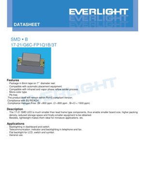
The 17-21/G6C-FP1Q1B/3T is a surface-mount device (SMD) LED utilizing AlGaInP chip technology to emit a Brilliant Yellow Green light. This component is designed for high-density PCB applications where space and weight are critical constraints. Its compact 1.6mm x 0.8mm x 0.6mm footprint enables significant reductions in board size and equipment dimensions compared to traditional lead-frame LEDs.
The LED is packaged on 8mm tape wound onto a 7-inch diameter reel, making it fully compatible with automated pick-and-place assembly equipment. It is qualified for standard infrared and vapor phase reflow soldering processes. The device is constructed as a mono-color type with a water-clear resin lens. It is manufactured as a Pb-free product and complies with key environmental regulations including RoHS, EU REACH, and Halogen-Free standards (Br <900 ppm, Cl <900 ppm, Br+Cl < 1500 ppm).
1.1 Core Advantages and Target Market
The primary advantage of this LED is its miniature size, which directly translates to higher packing density on PCBs, reduced storage space requirements, and ultimately, the development of smaller end-user equipment. Its lightweight construction further makes it ideal for portable and miniature electronic applications.
The target applications are diverse, focusing on indicator and backlighting functions. Key markets include automotive interiors (e.g., dashboard and switch backlighting), telecommunications equipment (e.g., indicator and backlighting in telephones and fax machines), and general electronics requiring flat backlighting for LCDs, switches, and symbols.
2. Technical Parameter Deep-Dive
2.1 Absolute Maximum Ratings
These ratings define the stress limits beyond which permanent damage to the device may occur. Operation under or at these limits is not guaranteed.
- Reverse Voltage (VR): 5V. Exceeding this voltage in reverse bias can cause junction breakdown.
- Forward Current (IF): 25 mA DC. The continuous operating current should not exceed this value.
- Peak Forward Current (IFP): 60 mA. This is permissible only under pulsed conditions with a duty cycle of 1/10 at 1 kHz.
- Power Dissipation (Pd): 60 mW. This is the maximum power the package can dissipate at an ambient temperature (Ta) of 25\u00b0C.
- Electrostatic Discharge (ESD): Human Body Model (HBM) rating of 2000V. Proper ESD handling procedures are mandatory.
- Operating Temperature (Topr): -40\u00b0C to +85\u00b0C. The device is guaranteed to function within this ambient temperature range.
- Storage Temperature (Tstg): -40\u00b0C to +90\u00b0C.
- Soldering Temperature (Tsol): For reflow soldering, a peak temperature of 260\u00b0C for a maximum of 10 seconds is specified. For hand soldering, the iron tip temperature must be below 350\u00b0C for a maximum of 3 seconds per terminal.
2.2 Electro-Optical Characteristics
These parameters are measured at Ta=25\u00b0C and define the typical performance of the device.
- Luminous Intensity (Iv): Ranges from 45.0 mcd (min) to 90.0 mcd (max) at a forward current (IF) of 20 mA. The typical value falls within this bin range.
- Viewing Angle (2\u03b81/2): A typical wide viewing angle of 140 degrees.
- Peak Wavelength (\u03bbp): Typically 575 nm.
- Dominant Wavelength (\u03bbd): Ranges from 570.0 nm (min) to 574.5 nm (max), defining the perceived color as Brilliant Yellow Green.
- Spectral Bandwidth (\u0394\u03bb): Typically 20 nm, measured at half the peak intensity (FWHM).
- Forward Voltage (VF): Ranges from 1.75 V (min) to 2.35 V (max) at IF=20 mA.
- Reverse Current (IR): Maximum of 10 \u03bcA when a reverse voltage (VR) of 5V is applied. Important Note: The device is not designed for operation in reverse bias; this test condition is for leakage current characterization only.
Tolerances: The datasheet specifies manufacturing tolerances: Luminous Intensity (\u00b111%), Dominant Wavelength (\u00b11 nm), and Forward Voltage (\u00b10.1 V).
3. Binning System Explanation
To ensure color and brightness consistency in production, LEDs are sorted into bins based on key parameters.
3.1 Luminous Intensity Binning
Bins are defined by codes P1, P2, and Q1, measured at IF=20 mA.
- P1: 45.0 \u2013 57.0 mcd
- P2: 57.0 \u2013 72.0 mcd
- Q1: 72.0 \u2013 90.0 mcd
3.2 Dominant Wavelength Binning
Bins are defined by codes CC2, CC3, and CC4, measured at IF=20 mA.
- CC2: 570.00 \u2013 571.50 nm
- CC3: 571.50 \u2013 573.00 nm
- CC4: 573.00 \u2013 574.50 nm
3.3 Forward Voltage Binning
Bins are defined by codes 0, 1, and 2, measured at IF=20 mA.
- 0: 1.75 \u2013 1.95 V
- 1: 1.95 \u2013 2.15 V
- 2: 2.15 \u2013 2.35 V
The specific part number 17-21/G6C-FP1Q1B/3T incorporates these bin codes, where \"FP1Q1B\" likely indicates specific intensity (Q1) and other characteristic bins.
4. Performance Curve Analysis
The datasheet references typical electro-optical characteristic curves. While not displayed in the provided text, such curves typically include:
- Relative Luminous Intensity vs. Forward Current (IF): Shows how light output increases with current, typically in a sub-linear relationship that saturates at higher currents.
- Forward Voltage vs. Forward Current (I-V Curve): Demonstrates the exponential relationship, crucial for designing current-limiting circuits.
- Relative Luminous Intensity vs. Ambient Temperature: Shows the decrease in light output as junction temperature rises, a key consideration for thermal management.
- Spectral Distribution: A plot of relative intensity versus wavelength, showing the peak at ~575 nm and the ~20 nm FWHM bandwidth.
These curves are essential for designers to predict performance under non-standard conditions (different currents, temperatures) and to optimize drive circuitry.
5. Mechanical and Package Information
5.1 Package Dimensions
The 17-21 SMD LED has a compact rectangular package. Key dimensions (in mm, tolerances \u00b10.1mm unless specified) include a body size of approximately 1.6mm in length, 0.8mm in width, and 0.6mm in height. The datasheet includes a detailed dimensioned drawing showing pad layout, component outline, and the location of the cathode identifier mark.
5.2 Polarity Identification
A clear cathode mark is indicated on the package drawing. Correct polarity must be observed during assembly to prevent reverse bias connection, which can damage the LED.
6. Soldering and Assembly Guidelines
6.1 Reflow Soldering Profile
A lead-free (Pb-free) reflow profile is specified:
- Pre-heating: 150\u00b0C to 200\u00b0C for 60-120 seconds.
- Time Above Liquidus (217\u00b0C): 60-150 seconds.
- Peak Temperature: Maximum of 260\u00b0C.
- Time Within 5\u00b0C of Peak: Maximum 10 seconds.
- Heating Rate: Maximum 6\u00b0C/second.
- Time Above 255\u00b0C: Maximum 30 seconds.
- Cooling Rate: Maximum 3\u00b0C/second.
Critical Notes: Reflow soldering should not be performed more than two times. No mechanical stress should be applied to the LED during heating. The circuit board should not be warped after soldering.
6.2 Hand Soldering
If hand soldering is necessary, use a soldering iron with a tip temperature below 350\u00b0C and a capacity less than 25W. Contact time per terminal must not exceed 3 seconds. Allow an interval of more than 2 seconds between soldering each terminal. Hand soldering carries a higher risk of thermal damage.
6.3 Storage and Moisture Sensitivity
The product is packaged in a moisture-resistant barrier bag with desiccant.
- Do not open the bag until ready for use.
- After opening, unused LEDs must be stored at \u2264 30\u00b0C and \u2264 60% Relative Humidity.
- The \"floor life\" after bag opening is 168 hours (7 days).
- If the exposure time is exceeded or the desiccant indicator has changed color, a bake-out at 60 \u00b1 5\u00b0C for 24 hours is required before reflow.
6.4 Repair
Repair after soldering is strongly discouraged. If absolutely unavoidable, a dual-head soldering iron must be used to simultaneously heat both terminals and avoid thermal stress. The impact on LED characteristics must be verified beforehand.
7. Packaging and Ordering Information
7.1 Reel and Tape Specifications
The LEDs are supplied in embossed carrier tape on 7-inch diameter reels. Each reel contains 3000 pieces. Detailed dimensioned drawings for the carrier tape pockets and the reel are provided, ensuring compatibility with automated feeders.
7.2 Label Explanation
The reel label contains several key fields: Customer's Product Number (CPN), Manufacturer's Product Number (P/N), Packing Quantity (QTY), Luminous Intensity Rank (CAT), Chromaticity/Dominant Wavelength Rank (HUE), Forward Voltage Rank (REF), and Lot Number (LOT No).
8. Application Suggestions and Design Considerations
8.1 Current Limiting is Mandatory
LEDs are current-driven devices. A series current-limiting resistor (or constant-current driver) is absolutely required. The forward voltage has a negative temperature coefficient and a manufacturing tolerance. A slight increase in supply voltage without current regulation can lead to a large, potentially destructive increase in forward current.
8.2 Thermal Management
While the package is small, power dissipation (max 60mW) and the derating of luminous intensity with temperature must be considered in high-ambient-temperature or high-current applications. Adequate PCB copper area for the LED pads can act as a heat sink.
8.3 ESD Protection
Although rated for 2000V HBM, implementing ESD protection diodes on sensitive signal lines connected to the LED anode/cathode is good practice, especially in handheld or frequently interfaced equipment.
9. Technical Comparison and Differentiation
The 17-21 package offers a significantly smaller footprint than traditional 3mm or 5mm round LEDs (e.g., 1.6x0.8mm vs. 5mm diameter). Compared to other SMD LEDs like the 0402 or 0603 sizes, the 17-21 may offer higher light output due to a potentially larger chip size within its package. The use of AlGaInP technology provides high efficiency in the yellow-green spectrum region compared to older technologies. Its compliance with Halogen-Free and REACH regulations makes it suitable for environmentally conscious designs required in modern electronics.
10. Frequently Asked Questions (Based on Technical Parameters)
Q: What resistor value should I use for a 5V supply?
A: Using Ohm's Law: R = (Vsupply - VF) / IF. For a typical VF of 2.0V at 20mA: R = (5 - 2.0) / 0.02 = 150 \u03a9. Always use the maximum VF from the bin (2.35V) to calculate the minimum resistor value to ensure current does not exceed 20mA: Rmin = (5 - 2.35) / 0.02 = 132.5 \u03a9 (use 150 \u03a9 or 180 \u03a9 standard value).
Q: Can I drive it with a 3.3V supply?
A: Yes, as the typical VF (1.75-2.35V) is below 3.3V. The calculation for the resistor would be: R = (3.3 - VF) / IF.
Q: Why is the viewing angle so wide (140\u00b0)?
A> The water-clear resin dome acts as a lens. The chip placement and dome shape are designed to provide a wide, Lambertian-like emission pattern, ideal for indicator applications where visibility from wide angles is needed.
Q: What does \"Brilliant Yellow Green\" mean in terms of chromaticity?
A: This is a descriptive name for the color defined by the dominant wavelength range of 570-574.5 nm. It sits between pure green (~555 nm) and pure yellow (~585 nm).
11. Design and Usage Case Study
Scenario: Designing a status indicator panel for a networking device.
The panel requires 10 independent status LEDs (Power, Link, Activity, etc.) in a very confined space on the front PCB. Using 5mm round LEDs would be impossible. The 17-21 SMD LED is selected. The designer creates a footprint per the datasheet's package drawing. A 5V rail is available on the board. The microcontroller GPIO pins can source 20mA. The designer calculates a 150\u03a9 current-limiting resistor for each LED (based on worst-case VF). The LEDs are placed on 0.1-inch (2.54mm) centers, allowing all 10 to fit in a row just 25.4mm long. The wide 140\u00b0 viewing angle ensures the indicators are visible even when viewing the panel from the side. The pick-and-place compatible tape and reel packaging allows for fully automated assembly, reducing manufacturing cost and time.
12. Technology Principle Introduction
This LED is based on AlGaInP (Aluminum Gallium Indium Phosphide) semiconductor material grown on a substrate. When a forward voltage is applied, electrons and holes are injected into the active region where they recombine, releasing energy in the form of photons (light). The specific ratio of aluminum, gallium, and indium in the crystal lattice determines the bandgap energy, which directly defines the wavelength (color) of the emitted light. For this Brilliant Yellow Green LED, the composition is tuned to produce photons with a wavelength centered around 575 nm. The water-clear epoxy resin encapsulant protects the semiconductor chip, acts as a lens to shape the light output beam, and provides mechanical stability.
13. Technology Trends
The general trend in indicator LEDs continues toward smaller package sizes (e.g., 01005, micro-LEDs) for ultra-high-density applications. There is also a strong drive toward higher efficiency (more lumens per watt) across all colors. For AlGaInP-based LEDs, research focuses on improving internal quantum efficiency and light extraction efficiency from the chip. Integration is another trend, with multi-color LEDs (RGB) or LED arrays becoming available in single, slightly larger SMD packages. Furthermore, the demand for broader environmental compliance (beyond RoHS to include full material declarations and lower carbon footprint) is influencing manufacturing processes and material choices.
LED Specification Terminology
Complete explanation of LED technical terms
Photoelectric Performance
| Term | Unit/Representation | Simple Explanation | Why Important |
|---|---|---|---|
| Luminous Efficacy | lm/W (lumens per watt) | Light output per watt of electricity, higher means more energy efficient. | Directly determines energy efficiency grade and electricity cost. |
| Luminous Flux | lm (lumens) | Total light emitted by source, commonly called "brightness". | Determines if the light is bright enough. |
| Viewing Angle | ° (degrees), e.g., 120° | Angle where light intensity drops to half, determines beam width. | Affects illumination range and uniformity. |
| CCT (Color Temperature) | K (Kelvin), e.g., 2700K/6500K | Warmth/coolness of light, lower values yellowish/warm, higher whitish/cool. | Determines lighting atmosphere and suitable scenarios. |
| CRI / Ra | Unitless, 0–100 | Ability to render object colors accurately, Ra≥80 is good. | Affects color authenticity, used in high-demand places like malls, museums. |
| SDCM | MacAdam ellipse steps, e.g., "5-step" | Color consistency metric, smaller steps mean more consistent color. | Ensures uniform color across same batch of LEDs. |
| Dominant Wavelength | nm (nanometers), e.g., 620nm (red) | Wavelength corresponding to color of colored LEDs. | Determines hue of red, yellow, green monochrome LEDs. |
| Spectral Distribution | Wavelength vs intensity curve | Shows intensity distribution across wavelengths. | Affects color rendering and quality. |
Electrical Parameters
| Term | Symbol | Simple Explanation | Design Considerations |
|---|---|---|---|
| Forward Voltage | Vf | Minimum voltage to turn on LED, like "starting threshold". | Driver voltage must be ≥Vf, voltages add up for series LEDs. |
| Forward Current | If | Current value for normal LED operation. | Usually constant current drive, current determines brightness & lifespan. |
| Max Pulse Current | Ifp | Peak current tolerable for short periods, used for dimming or flashing. | Pulse width & duty cycle must be strictly controlled to avoid damage. |
| Reverse Voltage | Vr | Max reverse voltage LED can withstand, beyond may cause breakdown. | Circuit must prevent reverse connection or voltage spikes. |
| Thermal Resistance | Rth (°C/W) | Resistance to heat transfer from chip to solder, lower is better. | High thermal resistance requires stronger heat dissipation. |
| ESD Immunity | V (HBM), e.g., 1000V | Ability to withstand electrostatic discharge, higher means less vulnerable. | Anti-static measures needed in production, especially for sensitive LEDs. |
Thermal Management & Reliability
| Term | Key Metric | Simple Explanation | Impact |
|---|---|---|---|
| Junction Temperature | Tj (°C) | Actual operating temperature inside LED chip. | Every 10°C reduction may double lifespan; too high causes light decay, color shift. |
| Lumen Depreciation | L70 / L80 (hours) | Time for brightness to drop to 70% or 80% of initial. | Directly defines LED "service life". |
| Lumen Maintenance | % (e.g., 70%) | Percentage of brightness retained after time. | Indicates brightness retention over long-term use. |
| Color Shift | Δu′v′ or MacAdam ellipse | Degree of color change during use. | Affects color consistency in lighting scenes. |
| Thermal Aging | Material degradation | Deterioration due to long-term high temperature. | May cause brightness drop, color change, or open-circuit failure. |
Packaging & Materials
| Term | Common Types | Simple Explanation | Features & Applications |
|---|---|---|---|
| Package Type | EMC, PPA, Ceramic | Housing material protecting chip, providing optical/thermal interface. | EMC: good heat resistance, low cost; Ceramic: better heat dissipation, longer life. |
| Chip Structure | Front, Flip Chip | Chip electrode arrangement. | Flip chip: better heat dissipation, higher efficacy, for high-power. |
| Phosphor Coating | YAG, Silicate, Nitride | Covers blue chip, converts some to yellow/red, mixes to white. | Different phosphors affect efficacy, CCT, and CRI. |
| Lens/Optics | Flat, Microlens, TIR | Optical structure on surface controlling light distribution. | Determines viewing angle and light distribution curve. |
Quality Control & Binning
| Term | Binning Content | Simple Explanation | Purpose |
|---|---|---|---|
| Luminous Flux Bin | Code e.g., 2G, 2H | Grouped by brightness, each group has min/max lumen values. | Ensures uniform brightness in same batch. |
| Voltage Bin | Code e.g., 6W, 6X | Grouped by forward voltage range. | Facilitates driver matching, improves system efficiency. |
| Color Bin | 5-step MacAdam ellipse | Grouped by color coordinates, ensuring tight range. | Guarantees color consistency, avoids uneven color within fixture. |
| CCT Bin | 2700K, 3000K etc. | Grouped by CCT, each has corresponding coordinate range. | Meets different scene CCT requirements. |
Testing & Certification
| Term | Standard/Test | Simple Explanation | Significance |
|---|---|---|---|
| LM-80 | Lumen maintenance test | Long-term lighting at constant temperature, recording brightness decay. | Used to estimate LED life (with TM-21). |
| TM-21 | Life estimation standard | Estimates life under actual conditions based on LM-80 data. | Provides scientific life prediction. |
| IESNA | Illuminating Engineering Society | Covers optical, electrical, thermal test methods. | Industry-recognized test basis. |
| RoHS / REACH | Environmental certification | Ensures no harmful substances (lead, mercury). | Market access requirement internationally. |
| ENERGY STAR / DLC | Energy efficiency certification | Energy efficiency and performance certification for lighting. | Used in government procurement, subsidy programs, enhances competitiveness. |