Table of Contents
- 1. Product Overview
- 1.1 Core Advantages and Product Positioning
- 1.2 Compliance and Environmental Specifications
- 2. In-Depth Technical Parameter Analysis
- 2.1 Absolute Maximum Ratings
- 2.2 Electro-Optical Characteristics (Ta=25°C)
- 2.3 Device Selection and Material Composition
- 3. Performance Curve Analysis
- 3.1 Forward Current vs. Forward Voltage (I-V Curve)
- 3.2 Luminous Intensity vs. Forward Current (L-I Curve)
- 3.3 Temperature Dependence
- 4. Mechanical and Packaging Information
- 4.1 Package Outline Dimensions
- 4.2 Polarity Identification
- 5. Soldering and Assembly Guidelines
- 5.1 Current Limiting Requirement
- 5.2 Storage and Moisture Sensitivity
- 5.3 Reflow Soldering Profile (Pb-free)
- 5.4 Hand Soldering and Rework
- 6. Packaging and Ordering Information
- 6.1 Standard Packaging
- 6.2 Label Explanation
- 7. Application Suggestions and Design Considerations
- 7.1 Typical Application Scenarios
- 7.2 Design Considerations
- 8. Technical Comparison and Differentiation
- 9. Frequently Asked Questions (Based on Technical Parameters)
- 9.1 What resistor value should I use with a 5V supply?
- 9.2 Can I drive this LED directly from a 3.3V microcontroller pin?
- 9.3 Why is the storage temperature higher than the operating temperature?
- 10. Practical Design and Usage Case
- 11. Operating Principle Introduction
- 12. Technology Trends and Context
- LED Specification Terminology
- Photoelectric Performance
- Electrical Parameters
- Thermal Management & Reliability
- Packaging & Materials
- Quality Control & Binning
- Testing & Certification
1. Product Overview
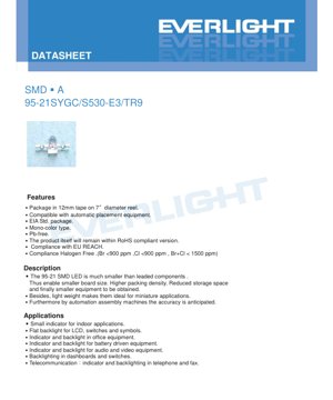
The 95-21SYGC/S530-E3/TR9 is a surface-mount device (SMD) LED designed for modern electronic applications requiring compact size, high reliability, and efficient performance. This component belongs to the family of miniature LEDs that have revolutionized indicator and backlighting solutions.
1.1 Core Advantages and Product Positioning
The primary advantage of this LED is its significantly reduced footprint compared to traditional leaded components. This miniaturization enables several key benefits for designers and manufacturers. Firstly, it allows for smaller printed circuit board (PCB) designs, which is critical in today's trend towards portable and miniaturized electronics. The higher packing density achievable with SMD components means more LEDs or other components can be placed in a given area, enhancing functionality without increasing size.
Secondly, the light weight of the SMD package makes it ideal for applications where mass is a concern, such as in handheld devices, wearables, and aerospace equipment. The use of automation-compatible tape and reel packaging (12mm tape on a 7-inch diameter reel) ensures high-speed, accurate placement using standard pick-and-place machines, reducing assembly time and cost while improving consistency. The product is positioned as a general-purpose indicator and backlight source for a wide range of consumer, office, and communication equipment.
1.2 Compliance and Environmental Specifications
This LED is manufactured with environmental and regulatory compliance as a priority. It is a Pb-free (lead-free) product, aligning with global restrictions on hazardous substances. The product itself remains within the compliant version of the RoHS (Restriction of Hazardous Substances) directive. It also complies with the EU REACH (Registration, Evaluation, Authorisation and Restriction of Chemicals) regulation. Furthermore, it is classified as Halogen Free, with strict limits on bromine (Br < 900 ppm), chlorine (Cl < 900 ppm), and their combined total (Br+Cl < 1500 ppm). These specifications make it suitable for markets with stringent environmental regulations.
2. In-Depth Technical Parameter Analysis
A thorough understanding of the electrical and optical parameters is essential for proper circuit design and ensuring long-term reliability.
2.1 Absolute Maximum Ratings
These ratings define the stress limits beyond which permanent damage to the device may occur. They are not intended for normal operation.
- Reverse Voltage (VR): 5V. Exceeding this voltage in reverse bias can cause junction breakdown.
- Continuous Forward Current (IF): 25mA. The DC current that can be applied continuously.
- Peak Forward Current (IFP): 60mA. This is the maximum allowable pulsed current, specified at a duty cycle of 1/10 and a frequency of 1kHz. It is crucial for multiplexing applications.
- Power Dissipation (Pd): 60mW. The maximum power the package can dissipate, calculated as Forward Voltage (VF) * Forward Current (IF).
- Operating & Storage Temperature: The device can operate from -40°C to +85°C and be stored from -40°C to +100°C.
- Electrostatic Discharge (ESD): 2000V (Human Body Model). Proper ESD handling procedures must be followed.
- Soldering Temperature: For reflow soldering, a peak temperature of 260°C for up to 10 seconds is specified. For hand soldering, the iron tip temperature should not exceed 350°C for 3 seconds per terminal.
2.2 Electro-Optical Characteristics (Ta=25°C)
These are the typical performance parameters under standard test conditions (20mA forward current, 25°C ambient).
- Luminous Intensity (Iv): 400mcd (Min), 630mcd (Typ). This is a measure of the perceived brightness of the light source. A ±11% tolerance is specified.
- Viewing Angle (2θ1/2): 25 degrees (Typical). This defines the angular spread at which the luminous intensity drops to half of its peak value. A 25° angle indicates a relatively focused beam, suitable for directed indicator lights.
- Peak Wavelength (λp): 575nm. The wavelength at which the spectral emission is strongest.
- Dominant Wavelength (λd): 573nm. This is the single wavelength perceived by the human eye, defining the color (brilliant yellow-green). A tolerance of ±1nm is specified.
- Spectrum Radiation Bandwidth (Δλ): 20nm. The spectral width at half the maximum intensity, indicating color purity.
- Forward Voltage (VF): 2.0V (Typ), 2.4V (Max) at 20mA. This is critical for designing the current-limiting resistor. The tolerance is ±0.1V.
- Reverse Current (IR): 10μA (Max) at VR=5V.
2.3 Device Selection and Material Composition
The LED chip is constructed from AlGaInP (Aluminum Gallium Indium Phosphide) semiconductor material. This material system is known for producing high-efficiency light in the yellow, orange, and red regions of the spectrum. The emitted color is brilliant yellow-green, and the resin encapsulating the chip is water clear, which maximizes light output and preserves the chip's color characteristics.
3. Performance Curve Analysis
The datasheet references typical electro-optical characteristic curves. While the specific graphs are not reproduced in text, their general implications are analyzed below based on standard LED behavior and the provided parameters.
3.1 Forward Current vs. Forward Voltage (I-V Curve)
For an AlGaInP LED like this one, the I-V curve exhibits a typical diode characteristic with a turn-on voltage slightly below the typical 2.0V. The curve will show an exponential increase in current once this knee voltage is exceeded. Designers must use a series resistor to set the operating current precisely at 20mA, as a small increase in voltage beyond the nominal VF can lead to a large, potentially destructive, increase in current.
3.2 Luminous Intensity vs. Forward Current (L-I Curve)
The light output (luminous intensity) is generally proportional to the forward current in the normal operating range (up to the rated 25mA). However, efficiency may drop at very high currents due to thermal effects. Operating at the typical 20mA ensures optimal performance and longevity.
3.3 Temperature Dependence
LED performance is temperature-sensitive. Typically, the forward voltage (VF) decreases with increasing junction temperature (a negative temperature coefficient). Conversely, the luminous intensity and dominant wavelength can shift. The specified operating temperature range of -40°C to +85°C indicates the device is designed to function across a wide environmental range, but designers should account for potential brightness and color shifts in extreme conditions.
4. Mechanical and Packaging Information
4.1 Package Outline Dimensions
The LED conforms to an industry-standard SMD package footprint. Key dimensions (with a general tolerance of ±0.1mm unless otherwise noted) define its size and solder pad layout. The package is designed for reliable surface mounting and good solder joint formation.
4.2 Polarity Identification
Proper polarity is essential for operation. The datasheet includes a diagram showing the cathode and anode terminals. Typically, the cathode may be marked by a notch, a green marking, or a different pad shape on the tape. Designers must consult the package diagram to correctly orient the component on the PCB footprint.
5. Soldering and Assembly Guidelines
Adherence to these guidelines is critical for assembly yield and long-term reliability.
5.1 Current Limiting Requirement
This is the most critical design rule: An external current-limiting resistor must always be used in series with the LED. The LED is a current-driven device. A slight increase in supply voltage above the LED's forward voltage will cause a large, uncontrolled increase in current, leading to rapid overheating and failure (burn-out). The resistor value is calculated using Ohm's Law: R = (V_supply - VF_LED) / I_desired.
5.2 Storage and Moisture Sensitivity
The LEDs are packaged in a moisture-resistant barrier bag with desiccant to prevent absorption of atmospheric moisture.
- Before Opening: Store at ≤30°C and ≤90% Relative Humidity (RH).
- After Opening: The "floor life" is 72 hours under conditions of ≤30°C and ≤60% RH. If not used within this time, unused parts must be resealed in a moisture-proof package with fresh desiccant.
- Baking: If the desiccant indicator shows saturation or the floor life is exceeded, the components must be baked at 60±5°C for 24 hours before use to drive out moisture and prevent "popcorning" during reflow soldering.
5.3 Reflow Soldering Profile (Pb-free)
A specific temperature profile is required for Pb-free solder alloys:
- Pre-heating: Ramp from ambient to 150-200°C over 60-120 seconds (max ramp rate 3°C/sec).
- Soak/Reflow: Time above liquidus (217°C): 60-150 seconds. Peak temperature must not exceed 260°C, and time above 255°C must not exceed 30 seconds. The component should be at peak temperature for a maximum of 10 seconds.
- Cooling: Maximum cool-down rate of 6°C/sec.
- Important: Reflow soldering should not be performed more than two times on the same board/component.
5.4 Hand Soldering and Rework
If hand soldering is necessary, extreme care is required. Use a soldering iron with a tip temperature ≤350°C and a power rating ≤25W. Contact time per terminal must be ≤3 seconds. Allow a cooling interval of at least 2 seconds between soldering each terminal. Avoid applying mechanical stress to the component during heating. Rework is strongly discouraged. If absolutely unavoidable, use a specialized double-head soldering iron to simultaneously heat both terminals and lift the component evenly to avoid damaging the solder pads or the LED itself.
6. Packaging and Ordering Information
6.1 Standard Packaging
The LEDs are supplied on embossed carrier tape sealed within a moisture-proof bag. The tape width is 12mm, wound on a standard 7-inch (178mm) diameter reel. Each reel contains 1000 pieces. Detailed dimensions for the carrier tape pockets and the reel are provided to ensure compatibility with automated assembly equipment.
6.2 Label Explanation
The packaging labels include several codes for traceability and binning:
- P/N: Product Number (95-21SYGC/S530-E3/TR9).
- LOT No: Manufacturing Lot Number for traceability.
- QTY: Packing Quantity (e.g., 1000).
- CAT: Luminous Intensity Rank (Binning for brightness).
- HUE: Dominant Wavelength Rank (Binning for color).
- REF: Forward Voltage Rank (Binning for VF).
7. Application Suggestions and Design Considerations
7.1 Typical Application Scenarios
Based on its specifications, this LED is well-suited for:
- Status Indicators: Power-on, standby, mode, or battery charge indicators in consumer electronics.
- Backlighting: For LCD panels in small devices, membrane switches, keypads, and instrument symbols.
- Office Equipment: Indicators and backlights in printers, scanners, copiers, and routers.
- Portable/Battery-Powered Devices: Ideal due to its low voltage (2.0V) and potential for efficient drive, extending battery life in phones, remote controls, and medical devices.
- Audio/Video Equipment: Display and function indicators on amplifiers, receivers, and set-top boxes.
- Automotive Interior: Backlighting for dashboard switches and controls (for non-critical illumination, noting the operating temperature range).
- Telecommunications: Indicator lights on telephones, fax machines, and network hardware.
7.2 Design Considerations
- Current Drive: Always use a constant current source or, more commonly, a voltage source with a series resistor. PWM (Pulse Width Modulation) can be used for dimming.
- Thermal Management: While the power is low (40mW at 20mA), ensure the PCB has adequate thermal relief, especially if multiple LEDs are clustered or if the ambient temperature is high.
- Optical Design: The 25° viewing angle provides a directed beam. For wider illumination, a diffuser lens or reflector may be needed in the housing.
- ESD Protection: Incorporate ESD protection diodes on sensitive input lines if the LED is user-accessible.
8. Technical Comparison and Differentiation
Compared to older through-hole LED technologies, this SMD LED offers superior size, weight, and assembly advantages. Within the SMD yellow-green LED segment, its key differentiators are its specific combination of a relatively high luminous intensity (630mcd) at a low forward current (20mA), a standard 2.0V forward voltage compatible with many logic-level voltages, and its compliance with modern environmental standards (RoHS, REACH, Halogen-Free). The AlGaInP chip technology provides good efficiency and color stability for the yellow-green spectrum.
9. Frequently Asked Questions (Based on Technical Parameters)
9.1 What resistor value should I use with a 5V supply?
Using the typical VF of 2.0V and desired IF of 20mA: R = (5V - 2.0V) / 0.020A = 150 Ohms. The nearest standard value is 150Ω. The power dissipated in the resistor is (3V * 0.02A) = 0.06W, so a standard 1/8W (0.125W) or 1/4W resistor is sufficient.
9.2 Can I drive this LED directly from a 3.3V microcontroller pin?
Possibly, but caution is needed. The typical VF is 2.0V, and a microcontroller GPIO pin can often source 20mA. However, you must verify the microcontroller's absolute maximum per-pin current and total port current. It is generally safer and more reliable to use the GPIO pin to control a transistor (e.g., a small NPN or a MOSFET) which then drives the LED with current from the main power rail.
9.3 Why is the storage temperature higher than the operating temperature?
The storage temperature (up to 100°C) refers to the non-operating, ambient temperature the component can withstand without degradation when no electrical power or current-induced heat is present. The operating temperature (up to 85°C) includes the additional heat generated by the LED's own power dissipation during use. The junction temperature during operation will be higher than the ambient, so the allowable ambient is lower to keep the junction within safe limits.
10. Practical Design and Usage Case
Scenario: Designing a multi-LED status panel for a portable data logger.
The device has a 3.7V Li-ion battery and needs 5 yellow-green LEDs to indicate recording, memory full, battery low, Bluetooth connection, and GPS lock. Using the 95-21SYGC LED, the designer would:
- Calculate the series resistor for each LED: R = (3.7V - 2.0V) / 0.020A = 85 Ohms. Use a standard 82Ω or 100Ω resistor, adjusting for desired brightness vs. battery life.
- Place the LEDs on the PCB with correct polarity according to the footprint diagram.
- Drive each LED via a GPIO pin of the system's microcontroller through the calculated resistor.
- In the firmware, implement logic to turn LEDs on/off or blink them as needed.
- Ensure the PCB layout provides some spacing between LEDs to prevent thermal coupling and includes a ground plane for stability.
- Specify that the assembly house follows the provided reflow soldering profile.
This approach yields a compact, reliable, and low-power indicator system suitable for the portable application.
11. Operating Principle Introduction
Light Emitting Diodes (LEDs) are semiconductor devices that emit light through a process called electroluminescence. When a forward voltage is applied across the p-n junction of the semiconductor material (in this case, AlGaInP), electrons from the n-type region and holes from the p-type region are injected into the junction region. These charge carriers recombine, releasing energy in the form of photons (light). The specific wavelength (color) of the emitted light is determined by the bandgap energy of the semiconductor material. AlGaInP has a bandgap that corresponds to light in the yellow, orange, and red parts of the visible spectrum. The "water clear" epoxy resin encapsulant protects the chip and acts as a lens, shaping the light output beam.
12. Technology Trends and Context
The component described represents a mature and widely adopted technology within the broader LED industry. Key ongoing trends influencing such components include:
- Further Miniaturization: While the 95-21 package is small, even smaller chip-scale package (CSP) LEDs are emerging for ultra-compact designs.
- Increased Efficiency: Continuous improvements in epitaxial growth and chip design lead to higher luminous efficacy (more light output per electrical watt), allowing for lower drive currents and reduced power consumption.
- Enhanced Reliability and Lifetime: Improvements in packaging materials and thermal management are extending operational lifetimes, making LEDs suitable for more critical applications.
- Integration: Trends include integrating multiple LED chips (RGB) into a single package or combining the LED with a driver IC for simplified system design.
- Stricter Compliance: Environmental regulations like RoHS and REACH continue to evolve, pushing manufacturers towards even cleaner material sets and processes.
This datasheet reflects a reliable, standardized component that sits at the intersection of these trends, offering a balance of performance, size, cost, and compliance for a vast array of electronic products.
LED Specification Terminology
Complete explanation of LED technical terms
Photoelectric Performance
| Term | Unit/Representation | Simple Explanation | Why Important |
|---|---|---|---|
| Luminous Efficacy | lm/W (lumens per watt) | Light output per watt of electricity, higher means more energy efficient. | Directly determines energy efficiency grade and electricity cost. |
| Luminous Flux | lm (lumens) | Total light emitted by source, commonly called "brightness". | Determines if the light is bright enough. |
| Viewing Angle | ° (degrees), e.g., 120° | Angle where light intensity drops to half, determines beam width. | Affects illumination range and uniformity. |
| CCT (Color Temperature) | K (Kelvin), e.g., 2700K/6500K | Warmth/coolness of light, lower values yellowish/warm, higher whitish/cool. | Determines lighting atmosphere and suitable scenarios. |
| CRI / Ra | Unitless, 0–100 | Ability to render object colors accurately, Ra≥80 is good. | Affects color authenticity, used in high-demand places like malls, museums. |
| SDCM | MacAdam ellipse steps, e.g., "5-step" | Color consistency metric, smaller steps mean more consistent color. | Ensures uniform color across same batch of LEDs. |
| Dominant Wavelength | nm (nanometers), e.g., 620nm (red) | Wavelength corresponding to color of colored LEDs. | Determines hue of red, yellow, green monochrome LEDs. |
| Spectral Distribution | Wavelength vs intensity curve | Shows intensity distribution across wavelengths. | Affects color rendering and quality. |
Electrical Parameters
| Term | Symbol | Simple Explanation | Design Considerations |
|---|---|---|---|
| Forward Voltage | Vf | Minimum voltage to turn on LED, like "starting threshold". | Driver voltage must be ≥Vf, voltages add up for series LEDs. |
| Forward Current | If | Current value for normal LED operation. | Usually constant current drive, current determines brightness & lifespan. |
| Max Pulse Current | Ifp | Peak current tolerable for short periods, used for dimming or flashing. | Pulse width & duty cycle must be strictly controlled to avoid damage. |
| Reverse Voltage | Vr | Max reverse voltage LED can withstand, beyond may cause breakdown. | Circuit must prevent reverse connection or voltage spikes. |
| Thermal Resistance | Rth (°C/W) | Resistance to heat transfer from chip to solder, lower is better. | High thermal resistance requires stronger heat dissipation. |
| ESD Immunity | V (HBM), e.g., 1000V | Ability to withstand electrostatic discharge, higher means less vulnerable. | Anti-static measures needed in production, especially for sensitive LEDs. |
Thermal Management & Reliability
| Term | Key Metric | Simple Explanation | Impact |
|---|---|---|---|
| Junction Temperature | Tj (°C) | Actual operating temperature inside LED chip. | Every 10°C reduction may double lifespan; too high causes light decay, color shift. |
| Lumen Depreciation | L70 / L80 (hours) | Time for brightness to drop to 70% or 80% of initial. | Directly defines LED "service life". |
| Lumen Maintenance | % (e.g., 70%) | Percentage of brightness retained after time. | Indicates brightness retention over long-term use. |
| Color Shift | Δu′v′ or MacAdam ellipse | Degree of color change during use. | Affects color consistency in lighting scenes. |
| Thermal Aging | Material degradation | Deterioration due to long-term high temperature. | May cause brightness drop, color change, or open-circuit failure. |
Packaging & Materials
| Term | Common Types | Simple Explanation | Features & Applications |
|---|---|---|---|
| Package Type | EMC, PPA, Ceramic | Housing material protecting chip, providing optical/thermal interface. | EMC: good heat resistance, low cost; Ceramic: better heat dissipation, longer life. |
| Chip Structure | Front, Flip Chip | Chip electrode arrangement. | Flip chip: better heat dissipation, higher efficacy, for high-power. |
| Phosphor Coating | YAG, Silicate, Nitride | Covers blue chip, converts some to yellow/red, mixes to white. | Different phosphors affect efficacy, CCT, and CRI. |
| Lens/Optics | Flat, Microlens, TIR | Optical structure on surface controlling light distribution. | Determines viewing angle and light distribution curve. |
Quality Control & Binning
| Term | Binning Content | Simple Explanation | Purpose |
|---|---|---|---|
| Luminous Flux Bin | Code e.g., 2G, 2H | Grouped by brightness, each group has min/max lumen values. | Ensures uniform brightness in same batch. |
| Voltage Bin | Code e.g., 6W, 6X | Grouped by forward voltage range. | Facilitates driver matching, improves system efficiency. |
| Color Bin | 5-step MacAdam ellipse | Grouped by color coordinates, ensuring tight range. | Guarantees color consistency, avoids uneven color within fixture. |
| CCT Bin | 2700K, 3000K etc. | Grouped by CCT, each has corresponding coordinate range. | Meets different scene CCT requirements. |
Testing & Certification
| Term | Standard/Test | Simple Explanation | Significance |
|---|---|---|---|
| LM-80 | Lumen maintenance test | Long-term lighting at constant temperature, recording brightness decay. | Used to estimate LED life (with TM-21). |
| TM-21 | Life estimation standard | Estimates life under actual conditions based on LM-80 data. | Provides scientific life prediction. |
| IESNA | Illuminating Engineering Society | Covers optical, electrical, thermal test methods. | Industry-recognized test basis. |
| RoHS / REACH | Environmental certification | Ensures no harmful substances (lead, mercury). | Market access requirement internationally. |
| ENERGY STAR / DLC | Energy efficiency certification | Energy efficiency and performance certification for lighting. | Used in government procurement, subsidy programs, enhances competitiveness. |