Table of Contents
- 1. Product Overview
- 2. Technical Parameter Deep Dive
- 2.1 Absolute Maximum Ratings
- 2.2 Electro-Optical Characteristics
- 3. Binning System Explanation
- 3.1 Luminous Intensity Binning
- 3.2 Dominant Wavelength Binning
- 4. Performance Curve Analysis
- 5. Mechanical and Package Information
- 5.1 Package Dimensions
- 5.2 Polarity Identification
- 6. Soldering and Assembly Guidelines
- 6.1 Reflow Soldering Profile
- 6.2 Hand Soldering
- 6.3 Storage and Moisture Sensitivity
- 6.4 Rework and Repair
- 7. Packaging and Ordering Information
- 7.1 Packaging Specifications
- 7.2 Label Information
- 8. Application Recommendations
- 8.1 Typical Application Scenarios
- 8.2 Design Considerations
- 9. Technical Comparison and Differentiation
- 10. Frequently Asked Questions (FAQs)
- 11. Practical Design and Usage Case
- 12. Operating Principle Introduction
- 13. Technology Trends
- 13.1 Application Restrictions Note
- LED Specification Terminology
- Photoelectric Performance
- Electrical Parameters
- Thermal Management & Reliability
- Packaging & Materials
- Quality Control & Binning
- Testing & Certification
1. Product Overview
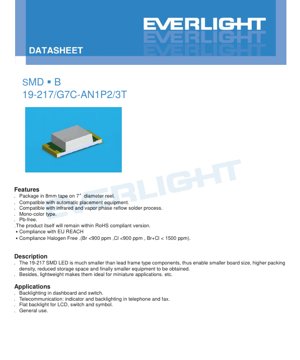
The 19-217/G7C-AN1P2/3T is a surface-mount device (SMD) LED designed for modern, compact electronic applications. It utilizes AlGaInP chip technology to produce a brilliant yellow-green light output. Its primary advantage lies in its miniature footprint, enabling significant reductions in printed circuit board (PCB) size and overall equipment dimensions. This contributes to higher packing density and reduced storage requirements. The component is lightweight, making it particularly suitable for applications where space and weight are critical constraints.
The LED is supplied in industry-standard 8mm tape on 7-inch diameter reels, ensuring compatibility with automated pick-and-place assembly equipment. It is formulated to be lead-free (Pb-free) and complies with major environmental regulations including RoHS, EU REACH, and halogen-free standards (Br <900 ppm, Cl <900 ppm, Br+Cl < 1500 ppm). The device is compatible with both infrared and vapor phase reflow soldering processes.
2. Technical Parameter Deep Dive
2.1 Absolute Maximum Ratings
These ratings define the limits beyond which permanent damage to the device may occur. Operation under these conditions is not guaranteed.
- Forward Current (IF): 25 mA (Continuous)
- Peak Forward Current (IFP): 60 mA (Duty Cycle 1/10 @ 1kHz)
- Power Dissipation (Pd): 60 mW
- Electrostatic Discharge (ESD) Human Body Model (HBM): 2000 V
- Operating Temperature (Topr): -40°C to +85°C
- Storage Temperature (Tstg): -40°C to +90°C
- Soldering Temperature (Tsol): Reflow: 260°C max for 10 seconds. Hand Soldering: 350°C max for 3 seconds.
2.2 Electro-Optical Characteristics
These parameters are measured at a standard test condition of Ta=25°C and IF=20mA, unless otherwise specified. They define the optical and electrical performance of the LED.
- Luminous Intensity (Iv): Ranges from 28.5 mcd (Min) to 72.0 mcd (Max). The typical value is not specified, indicating performance is managed through a binning system.
- Viewing Angle (2θ1/2): 120 degrees (Typical). This wide viewing angle makes the LED suitable for applications requiring broad illumination or visibility.
- Peak Wavelength (λp): 575 nm (Typical). This indicates the wavelength at which the emitted light intensity is highest.
- Dominant Wavelength (λd): Ranges from 569.5 nm to 577.5 nm. This is the single wavelength perceived by the human eye, defining the color.
- Spectral Bandwidth (Δλ): 20 nm (Typical). This defines the spread of the emitted spectrum around the peak wavelength.
- Forward Voltage (VF): Ranges from 1.7V (Min) to 2.4V (Max), with a typical value of 2.0V at 20mA.
- Reverse Current (IR): 10 μA (Max) at a Reverse Voltage (VR) of 5V. Important Note: The device is not designed for operation in reverse bias; this parameter is for leakage current testing only.
Tolerances: Luminous Intensity has a ±11% tolerance, and Dominant Wavelength has a ±1nm tolerance from the bin center values.
3. Binning System Explanation
To ensure consistent color and brightness in production, LEDs are sorted into bins based on measured performance.
3.1 Luminous Intensity Binning
LEDs are categorized into four bins (N1, N2, P1, P2) based on their measured luminous intensity at IF=20mA.
- Bin N1: 28.5 mcd to 36.0 mcd
- Bin N2: 36.0 mcd to 45.0 mcd
- Bin P1: 45.0 mcd to 57.0 mcd
- Bin P2: 57.0 mcd to 72.0 mcd
3.2 Dominant Wavelength Binning
LEDs are categorized into four bins (C16, C17, C18, C19) based on their dominant wavelength.
- Bin C16: 569.5 nm to 571.5 nm
- Bin C17: 571.5 nm to 573.5 nm
- Bin C18: 573.5 nm to 575.5 nm
- Bin C19: 575.5 nm to 577.5 nm
This two-dimensional binning (Intensity + Wavelength) allows designers to select components that meet specific brightness and color point requirements for their application, ensuring visual consistency across multiple LEDs.
4. Performance Curve Analysis
The datasheet references typical electro-optical characteristic curves. While the specific graphs are not detailed in the provided text, standard curves for such an LED would typically include:
- Relative Luminous Intensity vs. Forward Current (I-V Curve): Shows how light output increases with current, typically in a near-linear relationship within the operating range.
- Forward Voltage vs. Forward Current: Demonstrates the diode's exponential I-V characteristic.
- Relative Luminous Intensity vs. Ambient Temperature: Illustrates the decrease in light output as junction temperature rises, a critical factor for thermal management.
- Spectral Distribution: A plot showing the relative intensity of light emitted across different wavelengths, centered around the 575nm peak.
- Viewing Angle Pattern: A polar plot showing the angular distribution of light intensity.
These curves are essential for predicting real-world performance under non-standard conditions (different drive currents, temperatures) and for proper circuit design.
5. Mechanical and Package Information
5.1 Package Dimensions
The LED has a compact SMD package. Key dimensions (in mm, tolerance ±0.1mm unless noted) are:
- Package Length: 2.0 mm
- Package Width: 1.25 mm
- Package Height: 0.8 mm
- Land Pattern: The datasheet includes a detailed dimensional drawing specifying pad size, spacing, and component orientation for PCB layout. Correct land pattern design is crucial for reliable soldering and mechanical stability.
5.2 Polarity Identification
The cathode is typically marked on the device, often by a notch, a dot, or a green tint on the cathode side of the lens. The PCB footprint should be designed to match this polarity. Incorrect polarity connection will prevent the LED from illuminating and may stress the device.
6. Soldering and Assembly Guidelines
6.1 Reflow Soldering Profile
A lead-free (Pb-free) reflow profile is recommended:
- Pre-heating: 150–200°C for 60–120 seconds.
- Time Above Liquidus (217°C): 60–150 seconds.
- Peak Temperature: 260°C maximum.
- Time at Peak Temperature: 10 seconds maximum.
- Heating Rate: Maximum 6°C/second.
- Time Above 255°C: Maximum 30 seconds.
- Cooling Rate: Maximum 3°C/second.
Critical: Reflow soldering should not be performed more than two times on the same LED assembly.
6.2 Hand Soldering
If hand soldering is necessary, extreme care must be taken:
- Soldering iron tip temperature: < 350°C.
- Contact time per terminal: ≤ 3 seconds.
- Soldering iron capacity: ≤ 25W.
- Allow a minimum of 2 seconds between soldering each terminal to prevent heat buildup.
6.3 Storage and Moisture Sensitivity
The LEDs are packaged in moisture-resistant barrier bags with desiccant.
- Do not open the bag until ready for use.
- After opening, unused LEDs must be stored at ≤ 30°C and ≤ 60% Relative Humidity.
- The "floor life" after bag opening is 168 hours (7 days).
- If unused after this period, or if the desiccant indicator has changed color, the LEDs must be re-baked before use: 60 ±5°C for 24 hours.
6.4 Rework and Repair
Repair after soldering is strongly discouraged. If absolutely necessary, a specialized double-head soldering iron must be used to simultaneously heat both terminals, minimizing thermal stress. The impact on LED characteristics must be verified beforehand.
7. Packaging and Ordering Information
7.1 Packaging Specifications
The product is supplied for automated assembly:
- Carrier Tape: 8mm width.
- Reel: 7-inch (178mm) diameter.
- Quantity per Reel: 3000 pieces.
- Detailed dimensions for the carrier tape pockets and the reel are provided in the datasheet to ensure compatibility with feeder equipment.
7.2 Label Information
The reel label contains critical information for traceability and correct application:
- Customer Product Number (CPN)
- Product Number (P/N): e.g., 19-217/G7C-AN1P2/3T
- Packing Quantity (QTY)
- Luminous Intensity Rank (CAT) – corresponds to the Intensity Bin (N1, N2, P1, P2)
- Chromaticity/Dominant Wavelength Rank (HUE) – corresponds to the Wavelength Bin (C16-C19)
- Forward Voltage Rank (REF)
- Lot Number (LOT No.) for traceability
8. Application Recommendations
8.1 Typical Application Scenarios
- Backlighting: Dashboard indicators, switch illumination, keypad backlights.
- Telecommunications Equipment: Status indicators and backlighting for phones and fax machines.
- Flat Panel Backlighting: Edge-lighting for small LCD displays, backlighting for symbols and icons.
- General Indicator Use: Power status, mode indication, alert signals in consumer and industrial electronics.
8.2 Design Considerations
- Current Limiting: An external current-limiting resistor is MANDATORY. The LED's forward voltage has a range (1.7V-2.4V), and its I-V characteristic is exponential. A small change in supply voltage can cause a large, potentially destructive change in current without a series resistor. The resistor value (R) is calculated using Ohm's Law: R = (V_supply - VF_LED) / I_desired. Use the maximum VF from the datasheet for a conservative design.
- Thermal Management: While power dissipation is low (60mW max), ensuring the LED operates within its temperature rating is vital for long-term reliability and stable light output. Avoid placing it near other heat sources on the PCB.
- ESD Protection: Although rated for 2000V HBM, standard ESD handling precautions should be observed during assembly and handling.
9. Technical Comparison and Differentiation
The 19-217 LED differentiates itself primarily through its combination of a specific brilliant yellow-green color (using AlGaInP technology) and a very compact 2.0x1.25mm footprint. Compared to larger lead-frame LEDs, it offers significant space savings. Compared to other SMD colors, the AlGaInP technology typically offers higher luminous efficiency in the amber-yellow-green spectrum than older technologies. Its wide 120-degree viewing angle is a key feature for applications requiring broad visibility, as opposed to narrow-beam LEDs used for focused illumination.
10. Frequently Asked Questions (FAQs)
Q: Why is a current-limiting resistor absolutely necessary?
A: LEDs are current-driven devices. Their forward voltage is not a fixed value but has a manufacturing tolerance and varies with temperature. Connecting an LED directly to a voltage source, even one close to its typical VF, can result in excessive current flow, rapidly overheating and destroying the LED ("thermal runaway"). The series resistor provides a linear, predictable method to set the operating current.
Q: Can I drive this LED with a pulsed current higher than 25mA?
A: Yes, but only under specific conditions. The datasheet specifies a Peak Forward Current (IFP) of 60mA, but this is allowed only with a low duty cycle (1/10 or 10%) and at a frequency of 1kHz. Continuous operation above 25mA is not permitted and will exceed the power dissipation rating, leading to failure.
Q: What do the bin codes (e.g., P1, C18) mean for my design?
A: The bin codes ensure color and brightness consistency. If your product uses multiple LEDs and requires uniform appearance, you must specify and use LEDs from the same intensity and wavelength bins. Mixing bins may result in visibly different brightness or color shades between adjacent LEDs.
Q: How critical is the 7-day floor life after opening the moisture barrier bag?
A: It is very important for soldering reliability. SMD components can absorb moisture from the air. During reflow soldering, this trapped moisture can rapidly vaporize, causing internal delamination or "popcorning," which can crack the package and cause failure. Adhering to the storage and baking guidelines is essential for high-yield manufacturing.
11. Practical Design and Usage Case
Scenario: Designing a status indicator panel with 10 uniform yellow-green LEDs.
- Component Selection: Specify to your supplier that you require all LEDs from the same bin, e.g., Intensity Bin P1 (45-57 mcd) and Wavelength Bin C18 (573.5-575.5 nm). This is crucial for visual consistency.
- Circuit Design: Using a 5V supply and targeting a drive current of 20mA. Assuming a conservative VF of 2.4V (max), calculate the series resistor: R = (5V - 2.4V) / 0.020A = 130 Ohms. The nearest standard value is 130Ω or 120Ω. The power rating of the resistor: P = I^2 * R = (0.02^2) * 130 = 0.052W, so a standard 1/8W (0.125W) resistor is sufficient.
- PCB Layout: Use the exact land pattern from the datasheet's package dimension drawing. Ensure adequate spacing between LEDs for even light distribution and to avoid thermal coupling.
- Assembly: Keep the reel sealed until the production line is ready. Follow the reflow profile precisely. After assembly, avoid bending or flexing the PCB near the LEDs to prevent stress on the solder joints.
12. Operating Principle Introduction
This LED is based on AlGaInP (Aluminum Gallium Indium Phosphide) semiconductor material. When a forward voltage exceeding the diode's junction potential (approximately 1.7-2.4V) is applied, electrons and holes are injected into the active region of the semiconductor. These charge carriers recombine, releasing energy in the form of photons (light). The specific composition of the AlGaInP alloy determines the bandgap energy of the semiconductor, which directly dictates the wavelength (color) of the emitted light. In this case, the composition is tuned to produce photons in the yellow-green region of the visible spectrum, centered around 575 nanometers. The epoxy resin lens serves to protect the semiconductor chip, shape the light output beam (resulting in the 120-degree viewing angle), and enhance light extraction from the chip.
13. Technology Trends
The development of SMD LEDs like the 19-217 follows several key industry trends: Miniaturization continues to be a primary driver, enabling ever-smaller electronic devices. Increased Efficiency in materials like AlGaInP leads to higher luminous intensity from the same or smaller chip sizes. Environmental Compliance (RoHS, REACH, Halogen-Free) has become a standard requirement, not an option. Automation Compatibility through standardized tape-and-reel packaging is essential for high-volume, cost-effective manufacturing. Finally, there is a trend towards more precise and tighter Binning and Color Control to meet the demands of applications requiring high color consistency, such as full-color displays and automotive lighting, even though this particular component is a mono-color type.
13.1 Application Restrictions Note
The datasheet includes an important disclaimer regarding high-reliability applications. This product, as specified, may not be suitable for safety-critical systems such as automotive safety (e.g., brake lights), aerospace, military, or medical life-support equipment without additional qualification and possibly a different product grade. For such applications, consultation with the manufacturer is required to identify components designed and tested for the stringent reliability standards of those fields.
LED Specification Terminology
Complete explanation of LED technical terms
Photoelectric Performance
| Term | Unit/Representation | Simple Explanation | Why Important |
|---|---|---|---|
| Luminous Efficacy | lm/W (lumens per watt) | Light output per watt of electricity, higher means more energy efficient. | Directly determines energy efficiency grade and electricity cost. |
| Luminous Flux | lm (lumens) | Total light emitted by source, commonly called "brightness". | Determines if the light is bright enough. |
| Viewing Angle | ° (degrees), e.g., 120° | Angle where light intensity drops to half, determines beam width. | Affects illumination range and uniformity. |
| CCT (Color Temperature) | K (Kelvin), e.g., 2700K/6500K | Warmth/coolness of light, lower values yellowish/warm, higher whitish/cool. | Determines lighting atmosphere and suitable scenarios. |
| CRI / Ra | Unitless, 0–100 | Ability to render object colors accurately, Ra≥80 is good. | Affects color authenticity, used in high-demand places like malls, museums. |
| SDCM | MacAdam ellipse steps, e.g., "5-step" | Color consistency metric, smaller steps mean more consistent color. | Ensures uniform color across same batch of LEDs. |
| Dominant Wavelength | nm (nanometers), e.g., 620nm (red) | Wavelength corresponding to color of colored LEDs. | Determines hue of red, yellow, green monochrome LEDs. |
| Spectral Distribution | Wavelength vs intensity curve | Shows intensity distribution across wavelengths. | Affects color rendering and quality. |
Electrical Parameters
| Term | Symbol | Simple Explanation | Design Considerations |
|---|---|---|---|
| Forward Voltage | Vf | Minimum voltage to turn on LED, like "starting threshold". | Driver voltage must be ≥Vf, voltages add up for series LEDs. |
| Forward Current | If | Current value for normal LED operation. | Usually constant current drive, current determines brightness & lifespan. |
| Max Pulse Current | Ifp | Peak current tolerable for short periods, used for dimming or flashing. | Pulse width & duty cycle must be strictly controlled to avoid damage. |
| Reverse Voltage | Vr | Max reverse voltage LED can withstand, beyond may cause breakdown. | Circuit must prevent reverse connection or voltage spikes. |
| Thermal Resistance | Rth (°C/W) | Resistance to heat transfer from chip to solder, lower is better. | High thermal resistance requires stronger heat dissipation. |
| ESD Immunity | V (HBM), e.g., 1000V | Ability to withstand electrostatic discharge, higher means less vulnerable. | Anti-static measures needed in production, especially for sensitive LEDs. |
Thermal Management & Reliability
| Term | Key Metric | Simple Explanation | Impact |
|---|---|---|---|
| Junction Temperature | Tj (°C) | Actual operating temperature inside LED chip. | Every 10°C reduction may double lifespan; too high causes light decay, color shift. |
| Lumen Depreciation | L70 / L80 (hours) | Time for brightness to drop to 70% or 80% of initial. | Directly defines LED "service life". |
| Lumen Maintenance | % (e.g., 70%) | Percentage of brightness retained after time. | Indicates brightness retention over long-term use. |
| Color Shift | Δu′v′ or MacAdam ellipse | Degree of color change during use. | Affects color consistency in lighting scenes. |
| Thermal Aging | Material degradation | Deterioration due to long-term high temperature. | May cause brightness drop, color change, or open-circuit failure. |
Packaging & Materials
| Term | Common Types | Simple Explanation | Features & Applications |
|---|---|---|---|
| Package Type | EMC, PPA, Ceramic | Housing material protecting chip, providing optical/thermal interface. | EMC: good heat resistance, low cost; Ceramic: better heat dissipation, longer life. |
| Chip Structure | Front, Flip Chip | Chip electrode arrangement. | Flip chip: better heat dissipation, higher efficacy, for high-power. |
| Phosphor Coating | YAG, Silicate, Nitride | Covers blue chip, converts some to yellow/red, mixes to white. | Different phosphors affect efficacy, CCT, and CRI. |
| Lens/Optics | Flat, Microlens, TIR | Optical structure on surface controlling light distribution. | Determines viewing angle and light distribution curve. |
Quality Control & Binning
| Term | Binning Content | Simple Explanation | Purpose |
|---|---|---|---|
| Luminous Flux Bin | Code e.g., 2G, 2H | Grouped by brightness, each group has min/max lumen values. | Ensures uniform brightness in same batch. |
| Voltage Bin | Code e.g., 6W, 6X | Grouped by forward voltage range. | Facilitates driver matching, improves system efficiency. |
| Color Bin | 5-step MacAdam ellipse | Grouped by color coordinates, ensuring tight range. | Guarantees color consistency, avoids uneven color within fixture. |
| CCT Bin | 2700K, 3000K etc. | Grouped by CCT, each has corresponding coordinate range. | Meets different scene CCT requirements. |
Testing & Certification
| Term | Standard/Test | Simple Explanation | Significance |
|---|---|---|---|
| LM-80 | Lumen maintenance test | Long-term lighting at constant temperature, recording brightness decay. | Used to estimate LED life (with TM-21). |
| TM-21 | Life estimation standard | Estimates life under actual conditions based on LM-80 data. | Provides scientific life prediction. |
| IESNA | Illuminating Engineering Society | Covers optical, electrical, thermal test methods. | Industry-recognized test basis. |
| RoHS / REACH | Environmental certification | Ensures no harmful substances (lead, mercury). | Market access requirement internationally. |
| ENERGY STAR / DLC | Energy efficiency certification | Energy efficiency and performance certification for lighting. | Used in government procurement, subsidy programs, enhances competitiveness. |