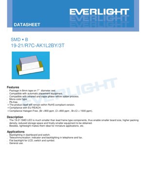
1. Product Overview
This document details the specifications for a surface-mount device (SMD) LED in the 19-21 package size, emitting a dark red color. This component is designed for modern electronic assembly processes, offering a compact footprint and reliable performance for various indicator and backlighting applications.
1.1 Core Advantages and Product Positioning
The primary advantage of this 19-21 SMD LED is its significantly reduced size compared to traditional lead-frame type LEDs. This miniaturization enables several key benefits for product designers:
- Smaller Board Size: Allows for more compact PCB designs.
- Higher Packing Density: More components can be placed in a given area.
- Reduced Storage Space: Smaller components require less inventory space.
- Lightweight Construction: Ideal for portable and miniature applications where weight is a critical factor.
- Compatibility: The device is packaged on 8mm tape on a 7-inch diameter reel, making it fully compatible with standard automatic pick-and-place equipment used in high-volume manufacturing.
The product is positioned as a general-purpose indicator and backlight solution, particularly suited for applications where space and weight are at a premium.
1.2 Target Market and Applications
This LED is designed for a broad range of electronic applications. Its key target markets include:
- Automotive Interior: Backlighting for dashboard instruments, switches, and control panels.
- Telecommunications: Status indicators and keypad backlighting in telephones, fax machines, and other communication devices.
- Consumer Electronics: Flat backlighting for LCD displays, symbol illumination, and switch backlighting.
- General Indicator Use: Any application requiring a reliable, compact red status or indicator light.
2. Technical Specifications Deep Dive
This section provides a detailed, objective analysis of the LED's technical parameters. Understanding these limits is crucial for reliable circuit design.
2.1 Absolute Maximum Ratings
These ratings define the stress limits beyond which permanent damage to the device may occur. Operation under or at these limits is not guaranteed and should be avoided for long-term reliability.
- Reverse Voltage (VR): 5V. Exceeding this voltage in reverse bias can cause immediate junction breakdown.
- Continuous Forward Current (IF): 25mA. The maximum DC current for continuous operation.
- Peak Forward Current (IFP): 60mA (Duty Cycle 1/10 @ 1kHz). This rating is for pulsed operation only and must not be exceeded even momentarily in DC operation.
- Power Dissipation (Pd): 60mW. The maximum power the package can dissipate as heat, calculated as VF * IF.
- Electrostatic Discharge (ESD) Human Body Model (HBM): 2000V. Provides a measure of the device's sensitivity to static electricity. Proper ESD handling procedures are mandatory.
- Operating Temperature (Topr): -40°C to +85°C. The ambient temperature range over which the device is specified to operate.
- Storage Temperature (Tstg): -40°C to +90°C.
- Soldering Temperature:
- Reflow Soldering: 260°C peak for a maximum of 10 seconds.
- Hand Soldering: 350°C at the iron tip for a maximum of 3 seconds per terminal.
2.2 Electro-Optical Characteristics (Ta=25°C)
These are the typical performance parameters measured under standard test conditions (25°C ambient, IF=5mA).
- Luminous Intensity (Iv): 7.2 mcd (Min) to 18.0 mcd (Max). The actual output is binned (see Section 3).
- Viewing Angle (2θ1/2): 100 degrees (Typical). This is the full angle at which the luminous intensity drops to half of its peak value.
- Peak Wavelength (λp): 639 nm (Typical). The wavelength at which the spectral emission is strongest.
- Dominant Wavelength (λd): 625.5 nm (Min) to 637.5 nm (Max). This is the single wavelength perceived by the human eye, defining the color. It is also binned.
- Spectral Bandwidth (Δλ): 20 nm (Typical). The width of the emission spectrum at half the maximum intensity.
- Forward Voltage (VF): 1.75V (Min) to 2.35V (Max) at IF=5mA. This parameter has a tight tolerance of ±0.1V and is binned.
- Reverse Current (IR): 10 μA (Max) at VR=5V. It is critical to note that the device is not designed for operation in reverse bias; this test is for leakage characterization only.
3. Binning System Explanation
To ensure consistent color and brightness in production, LEDs are sorted into bins based on key parameters. This allows designers to select parts that meet specific application requirements.
3.1 Luminous Intensity Binning
LEDs are categorized into four bins (K1, K2, L1, L2) based on their light output at 5mA.
- K1: 7.2 - 9.0 mcd
- K2: 9.0 - 11.5 mcd
- L1: 11.5 - 14.5 mcd
- L2: 14.5 - 18.0 mcd
A tolerance of ±11% applies within each bin.
3.2 Dominant Wavelength Binning
The color (hue) is controlled by binning the dominant wavelength into three ranges (E6, E7, E8).
- E6: 625.5 - 629.5 nm
- E7: 629.5 - 633.5 nm
- E8: 633.5 - 637.5 nm
A tolerance of ±1nm applies within each bin.
3.3 Forward Voltage Binning
To aid in current regulation design, especially in parallel strings, forward voltage is binned.
- Bin 0: 1.75 - 1.95 V
- Bin 1: 1.95 - 2.15 V
- Bin 2: 2.15 - 2.35 V
A tolerance of ±0.1V applies within each bin.
4. Performance Curve Analysis
The datasheet provides several characteristic curves that are essential for understanding the LED's behavior under non-standard conditions.
4.1 Luminous Intensity vs. Ambient Temperature
This curve shows that luminous intensity decreases as ambient temperature increases. This is a fundamental characteristic of semiconductor light sources due to reduced internal quantum efficiency at higher temperatures. Designers must derate the expected light output if the LED will operate in a high-temperature environment.
4.2 Luminous Intensity vs. Forward Current
The relationship between current (IF) and light output is generally linear at lower currents but can become sub-linear at higher currents due to heating and efficiency droop. Operating above the recommended current will not yield proportional increases in brightness and will reduce lifespan.
4.3 Forward Current vs. Forward Voltage (I-V Curve)
This is the fundamental diode characteristic. The curve shows an exponential relationship. A small change in voltage results in a large change in current, highlighting the critical need for current-limiting circuitry (e.g., a series resistor or constant current driver) to prevent thermal runaway and destruction.
4.4 Forward Current Derating Curve
This graph defines the maximum allowable continuous forward current as a function of ambient temperature. As temperature rises, the maximum safe current must be reduced to stay within the device's power dissipation limits and prevent overheating.
4.5 Spectrum Distribution
The spectral plot confirms the monochromatic nature of this AlGaInP-based LED, showing a narrow emission peak centered around 639 nm, which corresponds to a deep red color. The 20nm bandwidth indicates the spectral purity.
4.6 Radiation Pattern
The polar diagram illustrates the 100-degree viewing angle. The intensity is highest at 0 degrees (perpendicular to the LED face) and decreases symmetrically towards the edges, following a near-Lambertian pattern typical for this package style.
5. Mechanical and Package Information
5.1 Package Dimensions
The 19-21 SMD LED has the following key dimensions (tolerance ±0.1mm unless specified):
- Length: 2.0 mm
- Width: 1.25 mm
- Height: 0.8 mm
A cathode mark is clearly indicated on the package for correct polarity orientation during assembly.
5.2 Pad Design and Polarity
The recommended footprint (land pattern) is provided in the dimension drawing. Correct identification of the cathode (typically marked by a green tint, a notch, or a beveled corner as shown) is essential to prevent reverse connection during soldering.
6. Soldering and Assembly Guidelines
Adherence to these guidelines is critical for ensuring solder joint reliability and preventing damage to the LED.
6.1 Reflow Soldering Profile (Pb-free)
The recommended temperature profile is crucial for Pb-free (SAC) solder alloys:
- Pre-heating: 150-200°C for 60-120 seconds. This gradually heats the board to minimize thermal shock.
- Time Above Liquidus (217°C): 60-150 seconds.
- Peak Temperature: 260°C maximum.
- Time Within 5°C of Peak: 10 seconds maximum.
- Maximum Ramp-Up Rate: 6°C/second.
- Maximum Ramp-Down Rate: 3°C/second.
- Reflow Limit: The device should not undergo reflow soldering more than two times.
6.2 Hand Soldering Precautions
If hand soldering is necessary, extreme care must be taken:
- Use a temperature-controlled iron set to a maximum of 350°C.
- Limit contact time to 3 seconds per terminal.
- Use an iron with a power rating of 25W or less.
- Allow a minimum 2-second cooling interval between soldering each terminal.
- Avoid applying mechanical stress to the LED body during heating.
6.3 Rework and Repair
Repair after soldering is strongly discouraged. If absolutely unavoidable, a specialized double-head soldering iron must be used to simultaneously heat both terminals, allowing the component to be lifted without twisting. The potential for damage is high, and the characteristics of the LED should be verified after any rework.
7. Storage and Moisture Sensitivity
This component is moisture-sensitive. Improper handling can lead to \"popcorning\" (package cracking) during reflow due to rapid vapor expansion.
7.1 Storage Conditions
- Do not open the moisture-proof barrier bag until the components are ready for use.
- After opening: Store at ≤30°C and ≤60% Relative Humidity (RH).
- Floor Life: Use within 168 hours (7 days) of opening the bag.
- If not used within this time, reseal with desiccant or rebake.
7.2 Baking Instructions
If the desiccant indicator has changed color or the floor life has been exceeded, bake the components before use to remove absorbed moisture.
- Temperature: 60°C ±5°C
- Duration: 24 hours
- Note: Ensure the baking temperature does not exceed the maximum storage temperature (90°C).
8. Packaging and Ordering Information
8.1 Packaging Specifications
- Carrier Tape: 8mm width.
- Reel Size: 7-inch diameter.
- Quantity per Reel: 3000 pieces.
- Packaging: Components are sealed in an aluminum moisture-proof bag with desiccant and a humidity indicator card.
8.2 Label Explanation
The reel label contains critical information for traceability and identification:
- CPN: Customer's Part Number (if assigned).
- P/N: Manufacturer's Part Number (e.g., 19-21/R7C-AK1L2BY/3T).
- QTY: Packing quantity on the reel.
- CAT: Luminous Intensity bin code (e.g., K1, L2).
- HUE: Dominant Wavelength/Chromaticity bin code (e.g., E6, E7).
- REF: Forward Voltage bin code (e.g., 0, 1, 2).
- LOT No: Manufacturing lot number for traceability.
9. Application Design Considerations
9.1 Current Limiting is Mandatory
This is the single most important design rule. The LED must be driven with a constant current or have a series resistor calculated based on the supply voltage (Vsupply), the LED's forward voltage (VF from its bin), and the desired current (IF ≤ 25mA). The formula for the resistor is: R = (Vsupply - VF) / IF. Without this, a small increase in supply voltage will cause a large, potentially destructive increase in current.
9.2 Thermal Management
While the package is small, power dissipation (up to 60mW) generates heat. Ensure adequate PCB copper area (thermal relief pads) around the solder pads to help dissipate heat, especially if operating near maximum current or in high ambient temperatures. Refer to the derating curve.
9.3 ESD Protection
With an ESD HBM rating of 2000V, this device has moderate sensitivity. Implement ESD protection on input lines if they are exposed to user contact, and always follow standard ESD-safe handling procedures during assembly and prototyping.
10. Technical Comparison and Differentiation
The 19-21 package offers a specific balance of size and performance.
- vs. Larger SMD LEDs (e.g., 3528): The 19-21 is significantly smaller, saving board space, but typically has lower maximum current and light output ratings.
- vs. Smaller SMD LEDs (e.g., 0402): The 19-21 is easier to handle and solder manually, offers higher power handling, and often has a wider viewing angle.
- vs. Through-Hole LEDs: The SMD format eliminates the need for drilled holes, enables automated assembly, reduces weight, and allows for much higher component density on the PCB.
- AlGaInP Technology: This material system is known for high efficiency in the red/orange/amber color range, offering good brightness and color stability compared to older technologies.
11. Frequently Asked Questions (FAQ)
11.1 Can I drive this LED directly from a 3.3V or 5V supply?
No. You must use a series current-limiting resistor. For example, with a 5V supply and an LED with a VF of 2.0V at 20mA: R = (5V - 2.0V) / 0.020A = 150 Ω. A 150Ω resistor is required.
11.2 Why is the luminous intensity specified at 5mA instead of the maximum 25mA?
5mA is a standard test condition that allows for consistent comparison between different LED models and bins. You can operate it at higher currents (up to 25mA) for higher brightness, but you must refer to the \"Luminous Intensity vs. Forward Current\" curve and ensure thermal limits are not exceeded.
11.3 What do the bin codes (e.g., K1, E7, 1) mean for my design?
If your application requires consistent brightness across multiple LEDs, you should specify a tight luminous intensity bin (e.g., only L1). If color consistency is critical, specify a tight wavelength bin (e.g., only E7). For designs where LEDs are connected in parallel, specifying a tight forward voltage bin (e.g., only 1) helps ensure current sharing is more even.
11.4 The datasheet says \"not designed for reverse operation.\" What does this mean?
It means the LED should never be intentionally operated with the cathode at a higher voltage than the anode. The 5V reverse voltage rating is a maximum survivable rating for accidental transient events, not an operating condition. Permanent damage is likely if reverse voltage is applied during normal operation.
12. Design and Usage Case Study
Scenario: Designing a compact automotive switch with red backlighting.
- Component Selection: The 19-21 Dark Red LED is chosen for its small size, suitable brightness, and compatibility with automated assembly.
- Circuit Design: The vehicle's 12V system is used. A series resistor is calculated. Assuming a forward voltage bin of 2.0V and a desired current of 15mA for adequate brightness and long life: R = (12V - 2.0V) / 0.015A ≈ 667 Ω. A standard 680 Ω, 1/8W resistor is selected.
- PCB Layout: The compact 19-21 footprint is placed under the switch dome. A small amount of extra copper is added to the solder pads for heat dissipation.
- Manufacturing: LEDs from bin L1 (for consistent brightness) and E7 (for consistent color) are ordered on 7-inch reels for automated pick-and-place.
- Assembly: The sealed reel is used within its 7-day floor life. The PCB undergoes a single reflow pass using the specified Pb-free profile.
- Result: A reliable, uniformly lit switch backlight with a long operational lifespan.
13. Technology Principle Introduction
This LED is based on AlGaInP (Aluminum Gallium Indium Phosphide) semiconductor material grown on a substrate. When a forward voltage is applied across the p-n junction, electrons and holes are injected into the active region where they recombine. In a direct-bandgap semiconductor like AlGaInP, this recombination releases energy primarily in the form of photons (light). The specific ratio of aluminum, gallium, and indium in the crystal lattice determines the bandgap energy, which directly defines the wavelength (color) of the emitted light—in this case, deep red (~639 nm). The water-clear resin lens encapsulates the chip and shapes the emitted light into the specified 100-degree viewing angle.
LED Specification Terminology
Complete explanation of LED technical terms
Photoelectric Performance
| Term | Unit/Representation | Simple Explanation | Why Important |
|---|---|---|---|
| Luminous Efficacy | lm/W (lumens per watt) | Light output per watt of electricity, higher means more energy efficient. | Directly determines energy efficiency grade and electricity cost. |
| Luminous Flux | lm (lumens) | Total light emitted by source, commonly called "brightness". | Determines if the light is bright enough. |
| Viewing Angle | ° (degrees), e.g., 120° | Angle where light intensity drops to half, determines beam width. | Affects illumination range and uniformity. |
| CCT (Color Temperature) | K (Kelvin), e.g., 2700K/6500K | Warmth/coolness of light, lower values yellowish/warm, higher whitish/cool. | Determines lighting atmosphere and suitable scenarios. |
| CRI / Ra | Unitless, 0–100 | Ability to render object colors accurately, Ra≥80 is good. | Affects color authenticity, used in high-demand places like malls, museums. |
| SDCM | MacAdam ellipse steps, e.g., "5-step" | Color consistency metric, smaller steps mean more consistent color. | Ensures uniform color across same batch of LEDs. |
| Dominant Wavelength | nm (nanometers), e.g., 620nm (red) | Wavelength corresponding to color of colored LEDs. | Determines hue of red, yellow, green monochrome LEDs. |
| Spectral Distribution | Wavelength vs intensity curve | Shows intensity distribution across wavelengths. | Affects color rendering and quality. |
Electrical Parameters
| Term | Symbol | Simple Explanation | Design Considerations |
|---|---|---|---|
| Forward Voltage | Vf | Minimum voltage to turn on LED, like "starting threshold". | Driver voltage must be ≥Vf, voltages add up for series LEDs. |
| Forward Current | If | Current value for normal LED operation. | Usually constant current drive, current determines brightness & lifespan. |
| Max Pulse Current | Ifp | Peak current tolerable for short periods, used for dimming or flashing. | Pulse width & duty cycle must be strictly controlled to avoid damage. |
| Reverse Voltage | Vr | Max reverse voltage LED can withstand, beyond may cause breakdown. | Circuit must prevent reverse connection or voltage spikes. |
| Thermal Resistance | Rth (°C/W) | Resistance to heat transfer from chip to solder, lower is better. | High thermal resistance requires stronger heat dissipation. |
| ESD Immunity | V (HBM), e.g., 1000V | Ability to withstand electrostatic discharge, higher means less vulnerable. | Anti-static measures needed in production, especially for sensitive LEDs. |
Thermal Management & Reliability
| Term | Key Metric | Simple Explanation | Impact |
|---|---|---|---|
| Junction Temperature | Tj (°C) | Actual operating temperature inside LED chip. | Every 10°C reduction may double lifespan; too high causes light decay, color shift. |
| Lumen Depreciation | L70 / L80 (hours) | Time for brightness to drop to 70% or 80% of initial. | Directly defines LED "service life". |
| Lumen Maintenance | % (e.g., 70%) | Percentage of brightness retained after time. | Indicates brightness retention over long-term use. |
| Color Shift | Δu′v′ or MacAdam ellipse | Degree of color change during use. | Affects color consistency in lighting scenes. |
| Thermal Aging | Material degradation | Deterioration due to long-term high temperature. | May cause brightness drop, color change, or open-circuit failure. |
Packaging & Materials
| Term | Common Types | Simple Explanation | Features & Applications |
|---|---|---|---|
| Package Type | EMC, PPA, Ceramic | Housing material protecting chip, providing optical/thermal interface. | EMC: good heat resistance, low cost; Ceramic: better heat dissipation, longer life. |
| Chip Structure | Front, Flip Chip | Chip electrode arrangement. | Flip chip: better heat dissipation, higher efficacy, for high-power. |
| Phosphor Coating | YAG, Silicate, Nitride | Covers blue chip, converts some to yellow/red, mixes to white. | Different phosphors affect efficacy, CCT, and CRI. |
| Lens/Optics | Flat, Microlens, TIR | Optical structure on surface controlling light distribution. | Determines viewing angle and light distribution curve. |
Quality Control & Binning
| Term | Binning Content | Simple Explanation | Purpose |
|---|---|---|---|
| Luminous Flux Bin | Code e.g., 2G, 2H | Grouped by brightness, each group has min/max lumen values. | Ensures uniform brightness in same batch. |
| Voltage Bin | Code e.g., 6W, 6X | Grouped by forward voltage range. | Facilitates driver matching, improves system efficiency. |
| Color Bin | 5-step MacAdam ellipse | Grouped by color coordinates, ensuring tight range. | Guarantees color consistency, avoids uneven color within fixture. |
| CCT Bin | 2700K, 3000K etc. | Grouped by CCT, each has corresponding coordinate range. | Meets different scene CCT requirements. |
Testing & Certification
| Term | Standard/Test | Simple Explanation | Significance |
|---|---|---|---|
| LM-80 | Lumen maintenance test | Long-term lighting at constant temperature, recording brightness decay. | Used to estimate LED life (with TM-21). |
| TM-21 | Life estimation standard | Estimates life under actual conditions based on LM-80 data. | Provides scientific life prediction. |
| IESNA | Illuminating Engineering Society | Covers optical, electrical, thermal test methods. | Industry-recognized test basis. |
| RoHS / REACH | Environmental certification | Ensures no harmful substances (lead, mercury). | Market access requirement internationally. |
| ENERGY STAR / DLC | Energy efficiency certification | Energy efficiency and performance certification for lighting. | Used in government procurement, subsidy programs, enhances competitiveness. |