Table of Contents
- 1. Product Overview
- 2. In-Depth Technical Parameter Analysis
- 2.1 Absolute Maximum Ratings
- 2.2 Electro-Optical Characteristics
- 3. Binning System Explanation
- 3.1 R6 (Red) Wavelength Binning
- 3.2 GH (Green) Wavelength Binning
- 4. Performance Curve Analysis
- 4.1 R6 (Red Chip) Characteristics
- 4.2 GH (Green Chip) Characteristics
- 5. Mechanical & Package Information
- 5.1 Package Dimensions
- 5.2 Polarity Identification
- 6. Soldering & Assembly Guidelines
- 6.1 Reflow Soldering Profile
- 6.2 Storage & Handling Precautions
- 7. Packaging & Ordering Information
- 7.1 Reel and Tape Specifications
- 7.2 Label Information
- 8. Application Suggestions
- 8.1 Typical Application Scenarios
- 8.2 Design Considerations
- 9. Technical Comparison & Differentiation
- 10. Frequently Asked Questions (Based on Technical Parameters)
- 10.1 Can I drive this LED directly from a 5V supply without a resistor?
- 10.2 Why is the ESD rating different for the red and green chips?
- 10.3 What does the "binning" information mean for my design?
- 10.4 How many times can I reflow solder this component?
- 11. Practical Design Case Study
- 12. Operating Principle Introduction
- 13. Technology Trends
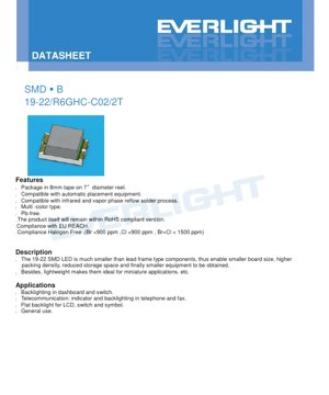
1. Product Overview
The 19-22/R6GHC-C02/2T is a compact, surface-mount device (SMD) LED designed for high-density electronic assemblies. This component integrates two distinct LED chip technologies within a single package: an AlGaInP chip for brilliant red emission (designated R6) and an InGaN chip for brilliant green emission (designated GH). This multi-color configuration provides design flexibility in a minimal footprint.
The primary advantage of this LED is its significantly reduced size compared to traditional lead-frame components. This miniaturization enables smaller printed circuit board (PCB) designs, higher component packing density, reduced storage requirements, and ultimately contributes to the development of more compact end-user equipment. Its lightweight construction further makes it an ideal choice for miniature and portable applications where space and weight are critical constraints.
The device is supplied in industry-standard 8mm tape on 7-inch diameter reels, ensuring compatibility with high-speed automated pick-and-place assembly equipment. It is formulated to be Pb-free and compliant with key environmental regulations including RoHS, EU REACH, and halogen-free standards (Br <900 ppm, Cl <900 ppm, Br+Cl < 1500 ppm).
2. In-Depth Technical Parameter Analysis
2.1 Absolute Maximum Ratings
Operating the device beyond these limits may cause permanent damage. All ratings are specified at an ambient temperature (Ta) of 25°C.
- Reverse Voltage (VR): 5 V (maximum). The device is not designed for reverse-bias operation; this rating is primarily for testing reverse leakage current (IR).
- Continuous Forward Current (IF): 25 mA for both the R6 (red) and GH (green) chips.
- Peak Forward Current (IFP): Applied under a duty cycle of 1/10 at 1 kHz. The R6 chip can handle 60 mA, while the GH chip is rated for 100 mA. This parameter is crucial for pulsed operation applications.
- Power Dissipation (Pd): The maximum allowable power dissipation is 60 mW for the R6 chip and 95 mW for the GH chip. This is a critical parameter for thermal management.
- Electrostatic Discharge (ESD) Human Body Model (HBM): The R6 chip offers robust ESD protection up to 2000V, whereas the GH chip is more sensitive with a rating of 150V. Proper ESD handling procedures are essential, especially for the green chip.
- Operating & Storage Temperature: The device is rated for operation from -40°C to +85°C and can be stored from -40°C to +90°C.
- Soldering Temperature: For reflow soldering, a peak temperature of 260°C for a maximum of 10 seconds is specified. For hand soldering, the iron tip temperature must not exceed 350°C for a maximum of 3 seconds per terminal.
2.2 Electro-Optical Characteristics
These parameters define the light output and electrical behavior under normal operating conditions (Ta=25°C, IF=5mA unless stated otherwise).
- Luminous Intensity (Iv): The R6 (red) chip has a typical intensity of 20.0 mcd (min. 14.5 mcd). The GH (green) chip has a typical intensity of 65.0 mcd (min. 45.0 mcd). A tolerance of ±11% applies.
- Viewing Angle (2θ1/2): A wide viewing angle of 130 degrees is typical for this package, providing broad illumination.
- Wavelength:
- R6 (Red): Peak Wavelength (λp) is 632 nm. Dominant Wavelength (λd) ranges from 617.5 nm to 629.5 nm, with a tolerance of ±1 nm. Spectral bandwidth (Δλ) is 20 nm.
- GH (Green): Peak Wavelength (λp) is 518 nm. Dominant Wavelength (λd) ranges from 517.5 nm to 533.5 nm, with a tolerance of ±1 nm. Spectral bandwidth (Δλ) is 35 nm.
- Forward Voltage (VF):
- R6 (Red): Typical 1.9 V, maximum 2.3 V at 5mA.
- GH (Green): Typical 2.9 V, maximum 3.4 V at 5mA.
- Reverse Current (IR): Measured at VR=5V. Maximum is 10 μA for R6 and 50 μA for GH.
3. Binning System Explanation
The LEDs are sorted (binned) based on their Dominant Wavelength to ensure color consistency within an application.
3.1 R6 (Red) Wavelength Binning
- Bin Code 1: 617.5 nm ≤ λd < 621.5 nm
- Bin Code 2: 621.5 nm ≤ λd < 625.5 nm
- Bin Code 3: 625.5 nm ≤ λd ≤ 629.5 nm
3.2 GH (Green) Wavelength Binning
- Bin Code 1: 517.5 nm ≤ λd < 525.5 nm
- Bin Code 2: 525.5 nm ≤ λd ≤ 533.5 nm
This binning information is critical for designers requiring precise color matching across multiple LEDs in a display or indicator panel.
4. Performance Curve Analysis
4.1 R6 (Red Chip) Characteristics
The provided curves illustrate key relationships:
- Relative Luminous Intensity vs. Forward Current: Shows the non-linear increase in light output with current. Operating above the recommended 5mA may yield higher intensity but impacts efficiency and lifetime.
- Relative Luminous Intensity vs. Ambient Temperature: Demonstrates the negative temperature coefficient of light output. Luminous intensity decreases as the junction temperature rises, which is a fundamental behavior of LED semiconductors.
- Forward Voltage vs. Forward Current: Depicts the diode's I-V characteristic curve.
- Peak Wavelength vs. Ambient Temperature: Shows a slight shift in the emitted wavelength with temperature.
4.2 GH (Green Chip) Characteristics
The curves for the green chip include:
- Spectrum Distribution: A plot of relative intensity versus wavelength, centered around 518 nm with a defined bandwidth.
- Forward Voltage vs. Forward Current: Similar to the red chip but with a higher knee voltage, typical for InGaN-based green LEDs.
- Forward Current Derating Curve: A vital graph showing the maximum allowable forward current as a function of ambient temperature. As temperature increases, the maximum current must be reduced to prevent overheating and ensure reliability.
- Radiation Diagram: Illustrates the spatial distribution of light intensity, confirming the 130-degree viewing angle.
- Relative Luminous Intensity vs. Forward Current & Ambient Temperature: These curves combine to show how light output depends on both drive current and operating temperature.
5. Mechanical & Package Information
5.1 Package Dimensions
The 19-22 SMD package has the following key dimensions (tolerance ±0.1mm):
- Length: 2.0 mm
- Width: 1.6 mm
- Height: 0.8 mm
- Lead spacing (pitch): 1.5 mm
- Pad size and shape are defined for reliable soldering.
5.2 Polarity Identification
The package features a polarity marking, typically a notch or a dot on the cathode side, to ensure correct orientation during assembly. The cathode is also associated with a specific pad shape in the recommended footprint.
6. Soldering & Assembly Guidelines
6.1 Reflow Soldering Profile
A lead-free reflow profile is specified:
- Pre-heating: 150–200°C for 60–120 seconds.
- Time Above Liquidus (217°C): 60–150 seconds.
- Peak Temperature: Maximum 260°C.
- Time Within 5°C of Peak: Maximum 10 seconds.
- Heating Rate: Maximum 6°C/sec.
- Time Above 255°C: Maximum 30 seconds.
- Cooling Rate: Maximum 3°C/sec.
6.2 Storage & Handling Precautions
- Moisture Sensitivity: The devices are packaged in a moisture-resistant barrier bag with desiccant. The bag must not be opened until the components are ready for use.
- Floor Life: After opening, LEDs should be used within 168 hours (7 days) if stored at ≤30°C and ≤60% RH. Unused parts must be resealed.
- Baking: If the exposure time is exceeded or the desiccant indicates moisture ingress, baking at 60 ±5°C for 24 hours is required before reflow.
- Current Limiting: An external current-limiting resistor is mandatory. LEDs exhibit an exponential current-voltage relationship, so a small voltage increase can cause a large, destructive current surge.
- Mechanical Stress: Avoid applying stress to the LED body during soldering or in the final application. Do not warp the PCB after assembly.
7. Packaging & Ordering Information
7.1 Reel and Tape Specifications
The product is supplied in a moisture-resistant packing system:
- Carrier Tape: 8mm width, with pockets designed for the 19-22 package.
- Reel: Standard 7-inch diameter reel.
- Quantity per Reel: 2000 pieces.
- Reel Dimensions: Outer diameter, hub diameter, and width are specified for compatibility with automated equipment.
7.2 Label Information
The reel label contains critical information for traceability and application:
- Customer Product Number (CPN)
- Product Number (P/N)
- Packing Quantity (QTY)
- Luminous Intensity Rank (CAT)
- Chromaticity & Wavelength Rank (HUE)
- Forward Voltage Rank (REF)
- Lot Number (LOT No)
8. Application Suggestions
8.1 Typical Application Scenarios
- Backlighting: Ideal for dashboard indicators, switch illumination, and symbol backlighting due to its small size and wide viewing angle.
- Telecommunication Equipment: Status indicators and keypad backlighting in telephones, fax machines, and other communication devices.
- LCD Flat Backlighting: Can be used in arrays to provide edge or direct backlighting for small LCD panels.
- General Purpose Indication: Power status, mode selection, and alert indicators in a wide range of consumer, industrial, and automotive electronics.
8.2 Design Considerations
- Drive Circuit: Always use a series resistor to set the forward current. Calculate the resistor value based on the supply voltage (Vs), the LED's forward voltage (VF), and the desired current (IF): R = (Vs - VF) / IF. Use the maximum VF from the datasheet for a conservative design.
- Thermal Management: Although small, power dissipation (Pd) must be considered, especially in high ambient temperatures or enclosed spaces. Adhere to the derating curve for the GH chip. Ensure adequate copper area on the PCB for heat sinking.
- ESD Protection: Implement ESD protection on input lines if the assembly process or end-use environment poses an ESD risk, particularly for the GH chip.
- Optical Design: The wide 130-degree viewing angle provides broad, diffuse light. For more focused light, external lenses or light guides may be necessary.
9. Technical Comparison & Differentiation
The 19-22/R6GHC-C02/2T offers several key advantages in its class:
- Dual-Chip/Multi-Color Capability: Integrating red and green in one package saves board space compared to using two separate single-color LEDs, simplifying design and assembly.
- Compact Footprint: The 2.0 x 1.6 mm footprint is among the smaller SMD LED packages, enabling high-density layouts.
- Robust Red Chip: The AlGaInP-based R6 chip offers high ESD immunity (2000V HBM), enhancing reliability in handling and operation.
- Environmental Compliance: Full compliance with RoHS, REACH, and halogen-free standards meets stringent global regulatory requirements for modern electronics.
- Automation Friendly: Tape-and-reel packaging and compatibility with IR/vapor phase reflow support cost-effective, high-volume manufacturing.
10. Frequently Asked Questions (Based on Technical Parameters)
10.1 Can I drive this LED directly from a 5V supply without a resistor?
No, this will destroy the LED. LEDs are current-driven devices. Connecting a 5V supply directly to the LED (especially the red chip with a typical VF of 1.9V) will cause a current far exceeding the 25mA maximum rating, leading to immediate failure. An external current-limiting resistor is absolutely mandatory.
10.2 Why is the ESD rating different for the red and green chips?
The difference stems from the underlying semiconductor materials. AlGaInP (red) structures are generally more robust against electrostatic discharge than InGaN (green/blue) structures. This is a fundamental material property. It necessitates careful ESD handling, particularly when working with the green chip.
10.3 What does the "binning" information mean for my design?
Binning ensures color consistency. If your application requires multiple LEDs to appear identical in color (e.g., an indicator bar), you should specify LEDs from the same wavelength bin code (HUE). Mixing bins may result in visibly different shades of red or green.
10.4 How many times can I reflow solder this component?
The datasheet specifies a maximum of two reflow soldering cycles. Each thermal cycle induces stress on the internal die attach and wire bonds. Exceeding two cycles increases the risk of latent reliability failures.
11. Practical Design Case Study
Scenario: Designing a dual-color (red/green) status indicator for a portable device powered by a 3.3V rail.
Design Steps:
- Selection: The 19-22/R6GHC-C02/2T is chosen for its dual-color capability and small size.
- Circuit Design: Two independent drive circuits are needed (one for red anode, one for green anode, common cathode).
- Resistor Calculation:
- For Red (R6, target IF=5mA, use max VF=2.3V for safety): R_red = (3.3V - 2.3V) / 0.005A = 200 Ω. Use a standard 200 Ω or 220 Ω resistor.
- For Green (GH, target IF=5mA, use max VF=3.4V): R_green = (3.3V - 3.4V) / 0.005A = -20 Ω. This calculation shows 3.3V is insufficient to drive the green chip at 5mA (VF typ. is 2.9V, but max is 3.4V). The supply voltage must be greater than the LED's forward voltage. A higher supply voltage (e.g., 5V) or a lower drive current would be required for the green LED.
- PCB Layout: Place the LED close to the board edge if it's an indicator. Use the recommended pad layout from the datasheet's dimension drawing. Include some small thermal relief on the cathode pad to aid soldering while providing a thermal path.
- Software Control: The microcontroller can independently control the red and green anodes to show red, green, or (by alternating rapidly) an amber/yellow color.
12. Operating Principle Introduction
Light Emitting Diodes (LEDs) are semiconductor p-n junction devices that emit light through a process called electroluminescence. When a forward voltage is applied across the p-n junction, electrons from the n-type region and holes from the p-type region are injected into the active region. When these charge carriers (electrons and holes) recombine, they release energy. In traditional semiconductors like silicon, this energy is released primarily as heat. In the direct bandgap semiconductor materials used in LEDs (AlGaInP for red/orange/yellow, InGaN for green/blue/white), a significant portion of this energy is released as photons (light). The specific wavelength (color) of the emitted light is determined by the bandgap energy of the semiconductor material, which is controlled by its precise chemical composition. The 19-22 device houses two such p-n junctions made from different materials within one package, allowing for two distinct colors of emission.
13. Technology Trends
The LED industry continues to evolve along several key trajectories relevant to components like the 19-22 SMD LED:
- Increased Efficiency: Ongoing improvements in internal quantum efficiency (IQE) and light extraction techniques lead to higher luminous intensity (mcd) for the same input current, or the same output with lower power consumption.
- Miniaturization: The drive for smaller end products pushes LED packages to ever-smaller footprints and lower profiles, following trends like 1.6x0.8mm and 1.0x0.5mm packages.
- Improved Color Consistency & Binning: Advances in epitaxial growth and manufacturing control reduce the natural variation in wavelength and intensity, leading to tighter bins and less need for sorting, or enabling more precise color mixing in RGB applications.
- Enhanced Reliability & Robustness: Research focuses on improving longevity under high-temperature operation and increasing ESD tolerance, particularly for sensitive InGaN-based green and blue chips.
- Integrated Solutions: A trend towards LEDs with built-in current-limiting resistors, protection diodes, or even driver ICs ("smart LEDs") to simplify circuit design and save board space.
LED Specification Terminology
Complete explanation of LED technical terms
Photoelectric Performance
| Term | Unit/Representation | Simple Explanation | Why Important |
|---|---|---|---|
| Luminous Efficacy | lm/W (lumens per watt) | Light output per watt of electricity, higher means more energy efficient. | Directly determines energy efficiency grade and electricity cost. |
| Luminous Flux | lm (lumens) | Total light emitted by source, commonly called "brightness". | Determines if the light is bright enough. |
| Viewing Angle | ° (degrees), e.g., 120° | Angle where light intensity drops to half, determines beam width. | Affects illumination range and uniformity. |
| CCT (Color Temperature) | K (Kelvin), e.g., 2700K/6500K | Warmth/coolness of light, lower values yellowish/warm, higher whitish/cool. | Determines lighting atmosphere and suitable scenarios. |
| CRI / Ra | Unitless, 0–100 | Ability to render object colors accurately, Ra≥80 is good. | Affects color authenticity, used in high-demand places like malls, museums. |
| SDCM | MacAdam ellipse steps, e.g., "5-step" | Color consistency metric, smaller steps mean more consistent color. | Ensures uniform color across same batch of LEDs. |
| Dominant Wavelength | nm (nanometers), e.g., 620nm (red) | Wavelength corresponding to color of colored LEDs. | Determines hue of red, yellow, green monochrome LEDs. |
| Spectral Distribution | Wavelength vs intensity curve | Shows intensity distribution across wavelengths. | Affects color rendering and quality. |
Electrical Parameters
| Term | Symbol | Simple Explanation | Design Considerations |
|---|---|---|---|
| Forward Voltage | Vf | Minimum voltage to turn on LED, like "starting threshold". | Driver voltage must be ≥Vf, voltages add up for series LEDs. |
| Forward Current | If | Current value for normal LED operation. | Usually constant current drive, current determines brightness & lifespan. |
| Max Pulse Current | Ifp | Peak current tolerable for short periods, used for dimming or flashing. | Pulse width & duty cycle must be strictly controlled to avoid damage. |
| Reverse Voltage | Vr | Max reverse voltage LED can withstand, beyond may cause breakdown. | Circuit must prevent reverse connection or voltage spikes. |
| Thermal Resistance | Rth (°C/W) | Resistance to heat transfer from chip to solder, lower is better. | High thermal resistance requires stronger heat dissipation. |
| ESD Immunity | V (HBM), e.g., 1000V | Ability to withstand electrostatic discharge, higher means less vulnerable. | Anti-static measures needed in production, especially for sensitive LEDs. |
Thermal Management & Reliability
| Term | Key Metric | Simple Explanation | Impact |
|---|---|---|---|
| Junction Temperature | Tj (°C) | Actual operating temperature inside LED chip. | Every 10°C reduction may double lifespan; too high causes light decay, color shift. |
| Lumen Depreciation | L70 / L80 (hours) | Time for brightness to drop to 70% or 80% of initial. | Directly defines LED "service life". |
| Lumen Maintenance | % (e.g., 70%) | Percentage of brightness retained after time. | Indicates brightness retention over long-term use. |
| Color Shift | Δu′v′ or MacAdam ellipse | Degree of color change during use. | Affects color consistency in lighting scenes. |
| Thermal Aging | Material degradation | Deterioration due to long-term high temperature. | May cause brightness drop, color change, or open-circuit failure. |
Packaging & Materials
| Term | Common Types | Simple Explanation | Features & Applications |
|---|---|---|---|
| Package Type | EMC, PPA, Ceramic | Housing material protecting chip, providing optical/thermal interface. | EMC: good heat resistance, low cost; Ceramic: better heat dissipation, longer life. |
| Chip Structure | Front, Flip Chip | Chip electrode arrangement. | Flip chip: better heat dissipation, higher efficacy, for high-power. |
| Phosphor Coating | YAG, Silicate, Nitride | Covers blue chip, converts some to yellow/red, mixes to white. | Different phosphors affect efficacy, CCT, and CRI. |
| Lens/Optics | Flat, Microlens, TIR | Optical structure on surface controlling light distribution. | Determines viewing angle and light distribution curve. |
Quality Control & Binning
| Term | Binning Content | Simple Explanation | Purpose |
|---|---|---|---|
| Luminous Flux Bin | Code e.g., 2G, 2H | Grouped by brightness, each group has min/max lumen values. | Ensures uniform brightness in same batch. |
| Voltage Bin | Code e.g., 6W, 6X | Grouped by forward voltage range. | Facilitates driver matching, improves system efficiency. |
| Color Bin | 5-step MacAdam ellipse | Grouped by color coordinates, ensuring tight range. | Guarantees color consistency, avoids uneven color within fixture. |
| CCT Bin | 2700K, 3000K etc. | Grouped by CCT, each has corresponding coordinate range. | Meets different scene CCT requirements. |
Testing & Certification
| Term | Standard/Test | Simple Explanation | Significance |
|---|---|---|---|
| LM-80 | Lumen maintenance test | Long-term lighting at constant temperature, recording brightness decay. | Used to estimate LED life (with TM-21). |
| TM-21 | Life estimation standard | Estimates life under actual conditions based on LM-80 data. | Provides scientific life prediction. |
| IESNA | Illuminating Engineering Society | Covers optical, electrical, thermal test methods. | Industry-recognized test basis. |
| RoHS / REACH | Environmental certification | Ensures no harmful substances (lead, mercury). | Market access requirement internationally. |
| ENERGY STAR / DLC | Energy efficiency certification | Energy efficiency and performance certification for lighting. | Used in government procurement, subsidy programs, enhances competitiveness. |