Table of Contents
- 1. Product Overview
- 1.1 Core Features and Advantages
- 1.2 Compliance and Environmental Specifications
- 1.3 Target Applications
- 2. Technical Parameter Deep-Dive
- 2.1 Absolute Maximum Ratings
- 2.2 Electro-Optical Characteristics
- 3. Binning System Explanation
- 3.1 Luminous Intensity Binning
- 3.2 Dominant Wavelength Binning
- 4. Performance Curve Analysis
- 5. Mechanical and Packaging Information
- 5.1 Package Dimensions
- 5.2 Polarity Identification
- 6. Soldering and Assembly Guide
- 6.1 Reflow Soldering Profile
- 6.2 Hand Soldering Instructions
- 6.3 Storage and Moisture Sensitivity
- 7. Packaging and Ordering Information
- 7.1 Reel and Tape Specifications
- 7.2 Label Explanation
- 8. Application Suggestions and Design Considerations
- 8.1 Circuit Design Considerations
- 8.2 Thermal Management
- 8.3 Optical Design
- 9. Precautions for Use
- 10. Technology Introduction and Context
- 10.1 Semiconductor Material
- 10.2 SMD Technology Advantage
- LED Specification Terminology
- Photoelectric Performance
- Electrical Parameters
- Thermal Management & Reliability
- Packaging & Materials
- Quality Control & Binning
- Testing & Certification
1. Product Overview
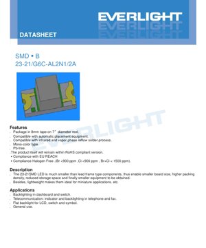
This document provides the complete technical specifications for a surface-mount device (SMD) LED identified as 23-21/G6C-AL2N1/2A. This component is a brilliant yellow LED designed for modern, compact electronic assemblies.
1.1 Core Features and Advantages
The primary advantages of this LED stem from its SMD package. It is significantly smaller than traditional lead-frame components, enabling higher board density, reduced equipment size, and minimized storage requirements. Its lightweight construction makes it ideal for miniature and portable applications. The device is packaged on 8mm tape wound on a 7-inch diameter reel, ensuring compatibility with standard automated pick-and-place equipment. It is designed for use with both infrared and vapor phase reflow soldering processes.
1.2 Compliance and Environmental Specifications
This product adheres to several key industry and environmental standards. It is a Pb-free (lead-free) component. The product itself remains compliant with the RoHS (Restriction of Hazardous Substances) directive. It also complies with EU REACH regulations and is classified as Halogen-Free, with Bromine (Br) and Chlorine (Cl) content each below 900 ppm and their combined total below 1500 ppm.
1.3 Target Applications
The 23-21 SMD LED is versatile and suitable for various illumination and indication purposes. Key application areas include backlighting for instrument panels, switches, and symbols; status indicators and backlighting in telecommunication devices such as telephones and fax machines; flat backlighting for LCD displays; and general-purpose indicator use.
2. Technical Parameter Deep-Dive
This section details the absolute limits and standard operating characteristics of the LED. All parameters are specified at an ambient temperature (Ta) of 25°C unless otherwise noted.
2.1 Absolute Maximum Ratings
Exceeding these ratings may cause permanent damage to the device. The maximum reverse voltage (VR) is 5V. The continuous forward current (IF) must not exceed 25 mA. A peak forward current (IFP) of 60 mA is permissible under pulsed conditions with a duty cycle of 1/10 at 1 kHz. The maximum power dissipation (Pd) is 60 mW. The device can withstand an electrostatic discharge (ESD) of 2000V per the Human Body Model (HBM). The operating temperature range (Topr) is from -40°C to +85°C, while the storage temperature range (Tstg) is from -40°C to +90°C. For soldering, a reflow profile with a peak of 260°C for 10 seconds or hand soldering at 350°C for 3 seconds is specified.
2.2 Electro-Optical Characteristics
These parameters define the light output and electrical behavior under normal operating conditions (IF=20mA). The luminous intensity (Iv) has a typical range, with minimum and maximum values defined by the binning system. The viewing angle (2θ1/2) is typically 130 degrees, indicating a wide radiation pattern. The peak wavelength (λp) is typically 575 nm, and the dominant wavelength (λd) ranges from 569.5 nm to 577.5 nm, corresponding to a brilliant yellow color. The spectral bandwidth (Δλ) is typically 20 nm. The forward voltage (VF) typically measures 2.0V, with a range from 1.70V to 2.40V. The reverse current (IR) is a maximum of 10 μA when a 5V reverse bias is applied. Important notes specify tolerances for luminous intensity (±11%) and dominant wavelength (±1 nm), and clarify that the 5V reverse rating is for IR testing only; the device is not designed for operation under reverse bias.
3. Binning System Explanation
To ensure color and brightness consistency, LEDs are sorted into bins. This device uses two independent binning parameters.
3.1 Luminous Intensity Binning
The luminous output is categorized into four bins (L2, M1, M2, N1) when driven at 20mA. The L2 bin ranges from 14.5 mcd to 18.0 mcd. The M1 bin covers 18.0 mcd to 22.5 mcd. The M2 bin spans 22.5 mcd to 28.5 mcd. The highest output bin, N1, ranges from 28.5 mcd to 36.0 mcd. The specific part number 23-21/G6C-AL2N1/2A indicates it belongs to the N1 bin for luminous intensity.
3.2 Dominant Wavelength Binning
The color, defined by dominant wavelength, is sorted into four bins (C16, C17, C18, C19). Bin C16 covers 569.5 nm to 571.5 nm. Bin C17 covers 571.5 nm to 573.5 nm. Bin C18 covers 573.5 nm to 575.5 nm. Bin C19 covers 575.5 nm to 577.5 nm. The part number suffix \"C\" likely correlates to one of these chromaticity bins, ensuring a specific yellow hue.
4. Performance Curve Analysis
Graphical data provides insight into the LED's behavior under varying conditions. The spectrum distribution curve shows the relative radiant power as a function of wavelength, centered around 575 nm with a typical width of 20 nm. The forward current vs. forward voltage (I-V) curve illustrates the exponential relationship, crucial for designing current-limiting circuits. The relative luminous intensity vs. ambient temperature curve demonstrates how light output decreases as temperature rises, which is critical for thermal management in designs. The relative luminous intensity vs. forward current curve shows the sub-linear increase in brightness with current, highlighting the point of diminishing returns and increased heat. The forward current derating curve specifies the maximum allowable continuous current as a function of ambient temperature to prevent overheating. The radiation diagram depicts the spatial distribution of light intensity, confirming the wide 130-degree viewing angle.
5. Mechanical and Packaging Information
5.1 Package Dimensions
The LED conforms to the 23-21 SMD package outline. Detailed dimensional drawings specify the length, width, height, pad sizes, and their positions. All unspecified tolerances are ±0.1 mm. This information is essential for PCB footprint design and ensuring proper placement and soldering.
5.2 Polarity Identification
The datasheet includes diagrams showing the cathode and anode markings on the device body, which are critical for correct orientation during assembly.
6. Soldering and Assembly Guide
6.1 Reflow Soldering Profile
A detailed temperature profile for Pb-free reflow soldering is provided. Key phases include: pre-heating between 150°C and 200°C for 60-120 seconds; a time above liquidus (217°C) of 60-150 seconds; a peak temperature not exceeding 260°C for a maximum of 10 seconds; and controlled ramp-up and cool-down rates (max 6°C/sec and 3°C/sec respectively). Reflow should not be performed more than two times.
6.2 Hand Soldering Instructions
If hand soldering is necessary, the soldering iron tip temperature must be below 350°C, and contact time per terminal must not exceed 3 seconds. A low-power iron (≤25W) is recommended. A minimum 2-second interval should be observed between soldering each terminal to prevent thermal damage.
6.3 Storage and Moisture Sensitivity
The LEDs are packaged in a moisture-resistant barrier bag with desiccant. The bag must not be opened until the components are ready for use. After opening, unused LEDs must be stored at ≤30°C and ≤60% Relative Humidity (RH) and used within 168 hours (7 days). If this window is exceeded or the desiccant indicates saturation, a bake-out at 60±5°C for 24 hours is required before use to prevent \"popcorning\" during reflow.
7. Packaging and Ordering Information
7.1 Reel and Tape Specifications
The components are supplied on embossed carrier tape with a width of 8mm, wound onto a 7-inch (178mm) diameter reel. Each reel contains 2000 pieces. Detailed drawings for the reel, carrier tape, and cover tape dimensions are provided, with standard tolerances of ±0.1mm.
7.2 Label Explanation
The reel label contains several key fields: CPN (Customer's Part Number), P/N (Manufacturer's Part Number, e.g., 23-21/G6C-AL2N1/2A), QTY (Packing Quantity), CAT (Luminous Intensity Bin, e.g., N1), HUE (Chromaticity/Dominant Wavelength Bin), REF (Forward Voltage Rank), and LOT No (Traceable Lot Number).
8. Application Suggestions and Design Considerations
8.1 Circuit Design Considerations
Current Limiting is Mandatory: LEDs are current-driven devices. A series resistor must always be used to limit the forward current to the recommended 20mA (or less). A slight increase in supply voltage can cause a large, potentially destructive increase in current due to the diode's exponential I-V characteristic.
8.2 Thermal Management
While the package is small, power dissipation (up to 60mW) and the negative temperature coefficient of luminous intensity must be considered. For continuous operation at high ambient temperatures, refer to the forward current derating curve. Adequate PCB copper area around the thermal pads can help dissipate heat.
8.3 Optical Design
The wide 130-degree viewing angle makes this LED suitable for applications requiring broad, even illumination rather than a focused beam. For backlighting panels or symbols, diffusers may be used to homogenize the light.
9. Precautions for Use
Key operational warnings are summarized: 1) Always use a current-limiting resistor. 2) Adhere strictly to moisture-sensitive device (MSD) handling procedures regarding storage and baking. 3) Follow the specified reflow or hand-soldering profiles precisely to avoid thermal damage. 4) Avoid mechanical stress on the component during and after soldering. 5) Repair after soldering is not recommended. If absolutely necessary, use a dual-tip soldering iron to simultaneously heat both terminals and lift the component to avoid pad damage, but verify device functionality afterwards as characteristics may be altered.
10. Technology Introduction and Context
10.1 Semiconductor Material
This LED utilizes an AlGaInP (Aluminum Gallium Indium Phosphide) semiconductor structure to produce brilliant yellow light. AlGaInP is known for high efficiency in the red to yellow-orange part of the visible spectrum. The resin lens is water-clear, allowing the pure color of the chip to be emitted without tinting.
10.2 SMD Technology Advantage
The transition from through-hole to Surface-Mount Technology for LEDs like the 23-21 package represents a significant advancement. It enables fully automated assembly, reduces parasitic inductance for high-speed applications, improves mechanical reliability by eliminating leads that can bend or break, and is essential for the ongoing miniaturization of electronic products.
LED Specification Terminology
Complete explanation of LED technical terms
Photoelectric Performance
| Term | Unit/Representation | Simple Explanation | Why Important |
|---|---|---|---|
| Luminous Efficacy | lm/W (lumens per watt) | Light output per watt of electricity, higher means more energy efficient. | Directly determines energy efficiency grade and electricity cost. |
| Luminous Flux | lm (lumens) | Total light emitted by source, commonly called "brightness". | Determines if the light is bright enough. |
| Viewing Angle | ° (degrees), e.g., 120° | Angle where light intensity drops to half, determines beam width. | Affects illumination range and uniformity. |
| CCT (Color Temperature) | K (Kelvin), e.g., 2700K/6500K | Warmth/coolness of light, lower values yellowish/warm, higher whitish/cool. | Determines lighting atmosphere and suitable scenarios. |
| CRI / Ra | Unitless, 0–100 | Ability to render object colors accurately, Ra≥80 is good. | Affects color authenticity, used in high-demand places like malls, museums. |
| SDCM | MacAdam ellipse steps, e.g., "5-step" | Color consistency metric, smaller steps mean more consistent color. | Ensures uniform color across same batch of LEDs. |
| Dominant Wavelength | nm (nanometers), e.g., 620nm (red) | Wavelength corresponding to color of colored LEDs. | Determines hue of red, yellow, green monochrome LEDs. |
| Spectral Distribution | Wavelength vs intensity curve | Shows intensity distribution across wavelengths. | Affects color rendering and quality. |
Electrical Parameters
| Term | Symbol | Simple Explanation | Design Considerations |
|---|---|---|---|
| Forward Voltage | Vf | Minimum voltage to turn on LED, like "starting threshold". | Driver voltage must be ≥Vf, voltages add up for series LEDs. |
| Forward Current | If | Current value for normal LED operation. | Usually constant current drive, current determines brightness & lifespan. |
| Max Pulse Current | Ifp | Peak current tolerable for short periods, used for dimming or flashing. | Pulse width & duty cycle must be strictly controlled to avoid damage. |
| Reverse Voltage | Vr | Max reverse voltage LED can withstand, beyond may cause breakdown. | Circuit must prevent reverse connection or voltage spikes. |
| Thermal Resistance | Rth (°C/W) | Resistance to heat transfer from chip to solder, lower is better. | High thermal resistance requires stronger heat dissipation. |
| ESD Immunity | V (HBM), e.g., 1000V | Ability to withstand electrostatic discharge, higher means less vulnerable. | Anti-static measures needed in production, especially for sensitive LEDs. |
Thermal Management & Reliability
| Term | Key Metric | Simple Explanation | Impact |
|---|---|---|---|
| Junction Temperature | Tj (°C) | Actual operating temperature inside LED chip. | Every 10°C reduction may double lifespan; too high causes light decay, color shift. |
| Lumen Depreciation | L70 / L80 (hours) | Time for brightness to drop to 70% or 80% of initial. | Directly defines LED "service life". |
| Lumen Maintenance | % (e.g., 70%) | Percentage of brightness retained after time. | Indicates brightness retention over long-term use. |
| Color Shift | Δu′v′ or MacAdam ellipse | Degree of color change during use. | Affects color consistency in lighting scenes. |
| Thermal Aging | Material degradation | Deterioration due to long-term high temperature. | May cause brightness drop, color change, or open-circuit failure. |
Packaging & Materials
| Term | Common Types | Simple Explanation | Features & Applications |
|---|---|---|---|
| Package Type | EMC, PPA, Ceramic | Housing material protecting chip, providing optical/thermal interface. | EMC: good heat resistance, low cost; Ceramic: better heat dissipation, longer life. |
| Chip Structure | Front, Flip Chip | Chip electrode arrangement. | Flip chip: better heat dissipation, higher efficacy, for high-power. |
| Phosphor Coating | YAG, Silicate, Nitride | Covers blue chip, converts some to yellow/red, mixes to white. | Different phosphors affect efficacy, CCT, and CRI. |
| Lens/Optics | Flat, Microlens, TIR | Optical structure on surface controlling light distribution. | Determines viewing angle and light distribution curve. |
Quality Control & Binning
| Term | Binning Content | Simple Explanation | Purpose |
|---|---|---|---|
| Luminous Flux Bin | Code e.g., 2G, 2H | Grouped by brightness, each group has min/max lumen values. | Ensures uniform brightness in same batch. |
| Voltage Bin | Code e.g., 6W, 6X | Grouped by forward voltage range. | Facilitates driver matching, improves system efficiency. |
| Color Bin | 5-step MacAdam ellipse | Grouped by color coordinates, ensuring tight range. | Guarantees color consistency, avoids uneven color within fixture. |
| CCT Bin | 2700K, 3000K etc. | Grouped by CCT, each has corresponding coordinate range. | Meets different scene CCT requirements. |
Testing & Certification
| Term | Standard/Test | Simple Explanation | Significance |
|---|---|---|---|
| LM-80 | Lumen maintenance test | Long-term lighting at constant temperature, recording brightness decay. | Used to estimate LED life (with TM-21). |
| TM-21 | Life estimation standard | Estimates life under actual conditions based on LM-80 data. | Provides scientific life prediction. |
| IESNA | Illuminating Engineering Society | Covers optical, electrical, thermal test methods. | Industry-recognized test basis. |
| RoHS / REACH | Environmental certification | Ensures no harmful substances (lead, mercury). | Market access requirement internationally. |
| ENERGY STAR / DLC | Energy efficiency certification | Energy efficiency and performance certification for lighting. | Used in government procurement, subsidy programs, enhances competitiveness. |