Table of Contents
- 1. Product Overview
- 1.1 Core Features and Advantages
- 2. Technical Parameter Deep-Dive Analysis
- 2.1 Absolute Maximum Ratings
- 2.2 Electro-Optical Characteristics at 25°C
- 3. Binning System Explanation
- 3.1 Luminous Intensity Binning
- 3.2 Forward Voltage Binning (Green & Blue only)
- 4. Performance Curve Analysis
- 4.1 Forward Current vs. Forward Voltage (I-V Curve)
- 4.2 Luminous Intensity vs. Forward Current
- 4.3 Luminous Intensity vs. Ambient Temperature
- 4.4 Forward Current Derating Curve
- 4.5 Spectral Distribution
- 4.6 Radiation Diagram (Viewing Angle Pattern)
- 5. Mechanical and Package Information
- 5.1 Package Dimensions
- 5.2 Suggested Pad Layout and Polarity Identification
- 6. Soldering and Assembly Guidelines
- 7. Packaging and Ordering Information
- 8. Application Suggestions
- 8.1 Typical Application Scenarios
- 8.2 Design Considerations and Notes
- 9. Technical Comparison and Differentiation
- 10. Frequently Asked Questions (Based on Technical Parameters)
- 11. Design and Usage Case Study
- 12. Technology Principle Introduction
- 13. Industry Trends and Developments
- LED Specification Terminology
- Photoelectric Performance
- Electrical Parameters
- Thermal Management & Reliability
- Packaging & Materials
- Quality Control & Binning
- Testing & Certification
1. Product Overview
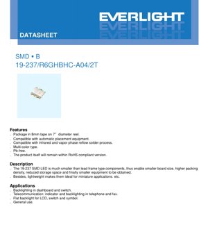
The 19-237 series is a compact, multi-color Surface Mount Device (SMD) LED designed for modern electronic applications requiring miniaturization and high reliability. This component is significantly smaller than traditional lead-frame type LEDs, enabling substantial reductions in PCB footprint, increased packing density, and minimized storage requirements. Its lightweight construction makes it particularly suitable for space-constrained and portable devices.
1.1 Core Features and Advantages
The key features that define this product family include its compatibility with standard 8mm tape on 7-inch diameter reels, making it fully suitable for automated pick-and-place assembly lines. It is designed to withstand both infrared and vapor phase reflow soldering processes, which are standard in high-volume electronics manufacturing. The series is offered in a multi-color configuration (Red, Green, Blue) and is manufactured as a Pb-free and RoHS-compliant product, ensuring environmental regulatory adherence.
The primary advantages stem from its miniature SMD package. This leads directly to smaller final product sizes, higher component density on circuit boards, and overall reductions in the size and weight of the end equipment. These characteristics are critical for applications in consumer electronics, automotive interiors, and communication devices.
2. Technical Parameter Deep-Dive Analysis
A thorough understanding of the electrical and optical specifications is essential for reliable circuit design and performance prediction.
2.1 Absolute Maximum Ratings
These ratings define the stress limits beyond which permanent damage to the device may occur. They are not intended for normal operation.
- Reverse Voltage (VR): 5V. Exceeding this voltage in reverse bias can cause junction breakdown.
- Continuous Forward Current (IF): 25 mA for all color types.
- Peak Forward Current (IFP): Varies by chip: 60 mA for Red (R6), 100 mA for Green (GH) and Blue (BH). This is specified at a duty cycle of 1/10 and 1 kHz frequency.
- Power Dissipation (Pd): 60 mW for Red (R6), 95 mW for Green (GH) and Blue (BH). This limit is crucial for thermal management.
- Electrostatic Discharge (ESD) Human Body Model (HBM): 2000V for Red (R6), 150V for Green (GH) and Blue (BH). This indicates the Red chip is more robust against ESD, while the Green and Blue chips require stricter handling precautions.
- Operating & Storage Temperature: -40°C to +85°C (operating), -40°C to +90°C (storage).
- Soldering Temperature: Reflow soldering at 260°C for 10 seconds maximum; hand soldering at 350°C for 3 seconds maximum.
2.2 Electro-Optical Characteristics at 25°C
These are the typical performance parameters measured under standard test conditions (Ta=25°C, IF=5mA).
- Luminous Intensity (Iv): Red (R6): 18.0-57.0 mcd; Green (GH): 28.5-112 mcd; Blue (BH): 11.5-28.5 mcd. The Green variant offers the highest typical output.
- Viewing Angle (2θ1/2): 120 degrees, typical. This wide viewing angle is suitable for indicator and backlighting applications.
- Peak Wavelength (λp): Red: 632 nm; Green: 518 nm; Blue: 468 nm.
- Dominant Wavelength (λd): Red: 613-627 nm; Green: 520-530 nm; Blue: 465-475 nm. This is the color perceived by the human eye.
- Spectral Bandwidth (Δλ): Red: 20 nm; Green: 35 nm; Blue: 25 nm. This indicates the spectral purity of the emitted light.
- Forward Voltage (VF): Red: 1.7-2.2V; Green & Blue: 2.6-3.0V. The lower VF of the Red LED is due to the different semiconductor material (AlGaInP vs. InGaN).
- Reverse Current (IR): Measured at VR=5V. Red: 10 μA max; Green: 50 μA max; Blue: 50 μA max.
Note on Tolerances: Luminous Intensity has a ±11% tolerance, Dominant Wavelength ±1nm, and Forward Voltage ±0.1V. These must be accounted for in design.
3. Binning System Explanation
The LEDs are sorted (binned) based on key parameters to ensure consistency within a production batch. This allows designers to select parts that meet specific brightness and electrical requirements.
3.1 Luminous Intensity Binning
Each color has specific bin codes defining a range of luminous intensity at IF=5mA.
- Red (R6): Bin M (18.0-28.5 mcd), N (28.5-45.0 mcd), P (45.0-57.0 mcd).
- Green (GH): Bin N (28.5-45.0 mcd), P (45.0-72.0 mcd), Q (72.0-112 mcd).
- Blue (BH): Bin L (11.5-18.0 mcd), M (18.0-28.5 mcd).
3.2 Forward Voltage Binning (Green & Blue only)
For the Green (GH) and Blue (BH) LEDs, an additional binning is performed on forward voltage.
- Bin 1: VF = 2.6 - 2.8V
- Bin 2: VF = 2.8 - 3.0V
This voltage binning is critical for applications where consistent current draw or battery life is a concern, especially when multiple LEDs are connected in parallel.
4. Performance Curve Analysis
The datasheet provides characteristic curves for each LED type (R6, GH, BH), illustrating performance under varying conditions.
4.1 Forward Current vs. Forward Voltage (I-V Curve)
The curves show the exponential relationship between current and voltage. The Red LED (R6) has a lower knee voltage (~1.8V) compared to the Green and Blue LEDs (~3.0V), consistent with their material differences. This curve is essential for designing the current-limiting circuitry.
4.2 Luminous Intensity vs. Forward Current
This graph demonstrates that light output increases approximately linearly with current in the typical operating range (up to ~20mA). However, operating above the recommended continuous current will reduce efficiency and lifespan due to increased heat.
4.3 Luminous Intensity vs. Ambient Temperature
All LEDs exhibit a decrease in light output as ambient temperature rises. The derating is significant, with output potentially dropping by over 50% as temperature approaches the maximum operating limit (+85°C). Proper thermal design on the PCB is necessary to maintain consistent brightness.
4.4 Forward Current Derating Curve
This critical curve dictates the maximum allowable continuous forward current as a function of ambient temperature. To ensure reliability, the operating current must be reduced as the ambient temperature increases beyond 25°C.
4.5 Spectral Distribution
The graphs display the relative intensity of light emitted across wavelengths. They confirm the peak and dominant wavelengths and show the spectral bandwidth, which affects color purity.
4.6 Radiation Diagram (Viewing Angle Pattern)
The polar plots visualize the spatial distribution of light intensity, confirming the 120-degree viewing angle. The pattern is roughly lambertian, meaning intensity is highest when viewed head-on and decreases at wider angles.
5. Mechanical and Package Information
5.1 Package Dimensions
The LED is housed in a compact surface-mount package with the following key dimensions (in mm): Length: 2.0 ±0.2, Width: 1.4 ±0.2, Height: 0.9. The cathode is identified by a marking on the package. The dimensional drawing includes critical features such as the lens shape and lead positions.
5.2 Suggested Pad Layout and Polarity Identification
A suggested PCB land pattern (pad layout) is provided for reference: Pad width: 0.8mm, Pad length: 1.35mm, Gap between pads: 0.35mm. Designers are advised to modify this based on their specific assembly process and thermal requirements. Clear identification of the anode and cathode pads is crucial to prevent reverse-bias installation.
6. Soldering and Assembly Guidelines
Adherence to soldering specifications is vital for long-term reliability and to prevent damage to the LED epoxy lens or semiconductor die.
- Reflow Soldering: Maximum peak temperature of 260°C for a duration not exceeding 10 seconds. A standard lead-free reflow profile is applicable.
- Hand Soldering: If necessary, the iron tip temperature should not exceed 350°C, and contact time should be limited to 3 seconds per lead. Use a heat sink if possible.
- Storage: Components are packed in moisture-resistant bags. Once opened, they should be used within a specified time frame or baked according to IPC standards if exposed to ambient humidity, to prevent \"popcorning\" during reflow.
7. Packaging and Ordering Information
The product is supplied on 8mm wide embossed carrier tape wound on 7-inch diameter reels, compatible with automated assembly equipment. The reel has standard dimensions: Reel Outer Diameter: 180.0mm, Reel Width: 12.4mm, Hub Hole Diameter: 44.0mm.
The label on the reel contains essential information for traceability and identification, including fields for Product Number, Quantity, Luminous Intensity Rank (CAT), Chromaticity/Wavelength Rank (HUE), Forward Voltage Rank (REF), and Lot Number. The specific part number 19-237/R6GHBHC-A04/2T follows a coding system indicating the series, color mix (R6=Red, GH=Green, BH=Blue), and likely binning or variant codes.
8. Application Suggestions
8.1 Typical Application Scenarios
- Backlighting: Ideal for backlighting switches, symbols, and small LCD panels in automotive dashboards, industrial controls, and consumer appliances.
- Status Indicators: Perfect for power, connectivity, and function status indicators in telecommunications equipment (phones, faxes, routers), computer peripherals, and medical devices.
- General Purpose Illumination: Suitable for any application requiring a small, reliable, low-power colored light source.
8.2 Design Considerations and Notes
- Current Limiting: Always use a series current-limiting resistor or constant-current driver. Calculate the resistor value based on the supply voltage, the LED's forward voltage (use max VF for a safe design), and the desired forward current (e.g., 5-20mA).
- Thermal Management: Although low power, heat dissipation must be considered, especially at higher currents or in high ambient temperatures. Ensure adequate copper area on the PCB connected to the LED's thermal pad (if any) or leads.
- ESD Protection: Implement ESD protection measures on the PCB input lines and enforce proper handling procedures during assembly, particularly for the Green and Blue variants which have a lower ESD rating.
- Optical Design: The wide 120-degree viewing angle provides good off-axis visibility. For focused light, external lenses or light guides may be required.
9. Technical Comparison and Differentiation
The 19-237 series differentiates itself through its combination of a very compact footprint (2.0x1.4mm), a standardized wide-viewing-angle package, and the availability of three primary colors from a single package family. Compared to larger SMD LEDs or through-hole LEDs, it offers superior space savings. The provision of detailed binning data for both luminous intensity and forward voltage (for Green/Blue) offers designers greater control over color consistency and electrical performance in their end products, which is a key advantage in applications requiring uniform appearance or precise power management.
10. Frequently Asked Questions (Based on Technical Parameters)
Q1: Can I drive this LED at 25mA continuously?
A1: While the Absolute Maximum Rating is 25mA, continuous operation at this current will generate maximum heat and may reduce lifespan. For optimal reliability and efficiency, design for a typical operating current of 5-20mA, as used in the specification tables, and refer to the forward current derating curve for elevated temperatures.
Q2: Why is the ESD rating different for the Red LED compared to the Green and Blue?
A2: The different semiconductor materials (AlGaInP for Red, InGaN for Green/Blue) have inherent differences in their sensitivity to electrostatic discharge. The InGaN-based chips are generally more susceptible, necessitating stricter handling (150V HBM vs. 2000V HBM).
Q3: How do I interpret the binning codes when ordering?
A3: Specify the desired luminous intensity bin (e.g., \"GH in Bin Q\" for brightest Green) and, for Green/Blue, the forward voltage bin (e.g., \"BH in Bin M, VF Bin 1\"). This ensures you receive LEDs with performance within the specified narrow ranges.
Q4: What is the difference between Peak Wavelength and Dominant Wavelength?
A4: Peak Wavelength (λp) is the wavelength at which the emitted optical power is maximum. Dominant Wavelength (λd) is the single wavelength of monochromatic light that matches the perceived color of the LED. λd is more relevant for color specification.
11. Design and Usage Case Study
Scenario: Designing a multi-status indicator panel for a portable medical device.
The panel requires Red (Error), Green (Ready), and Blue (Active) indicators. The 19-237 series is selected for its small size, allowing three LEDs to fit in a tight space. The designer chooses:
- R6 in Bin N for consistent medium-brightness red.
- GH in Bin P, VF Bin 1 for bright green with lower voltage drop to match power supply constraints.
- BH in Bin M, VF Bin 1 for blue.
A single 3.3V supply rail is used. Separate current-limiting resistors are calculated for each color: a smaller resistor for the Red LED (lower VF) and larger, identical resistors for the Green and Blue LEDs (similar VF). The PCB layout includes a small thermal relief pad connected to each cathode lead to aid heat dissipation. ESD protection diodes are placed on the signal lines leading to the LED drivers.
12. Technology Principle Introduction
Light emission in these LEDs is based on electroluminescence in semiconductor materials. When a forward voltage is applied across the p-n junction, electrons and holes are injected into the active region. Their recombination releases energy in the form of photons (light). The color of the light is determined by the bandgap energy of the semiconductor material:
- Red (R6): Uses an AlGaInP (Aluminum Gallium Indium Phosphide) compound semiconductor, which has a bandgap corresponding to red/orange light.
- Green & Blue (GH, BH): Use InGaN (Indium Gallium Nitride) with different indium/gallium ratios to tune the bandgap for green and blue light, respectively. Achieving efficient blue and green emission with InGaN was a significant technological advancement.
13. Industry Trends and Developments
The market for SMD LEDs like the 19-237 series continues to be driven by the demand for miniaturization, energy efficiency, and high reliability across all electronics sectors. Trends include:
- Increased Efficiency: Ongoing material science and epitaxial growth improvements lead to higher luminous efficacy (more light output per electrical watt).
- Improved Color Consistency: Tighter binning tolerances and advanced manufacturing controls ensure better color uniformity within and across production batches.
- Enhanced Reliability: Improvements in package materials (epoxy, silicone) and die attach technologies lead to longer operational lifetimes and better performance under high temperature and humidity.
- Integration: A trend towards integrating multiple LED chips (RGB, RGBW) into a single package for full-color applications, though discrete components like the 19-237 remain essential for cost-effective single-color solutions.
LED Specification Terminology
Complete explanation of LED technical terms
Photoelectric Performance
| Term | Unit/Representation | Simple Explanation | Why Important |
|---|---|---|---|
| Luminous Efficacy | lm/W (lumens per watt) | Light output per watt of electricity, higher means more energy efficient. | Directly determines energy efficiency grade and electricity cost. |
| Luminous Flux | lm (lumens) | Total light emitted by source, commonly called "brightness". | Determines if the light is bright enough. |
| Viewing Angle | ° (degrees), e.g., 120° | Angle where light intensity drops to half, determines beam width. | Affects illumination range and uniformity. |
| CCT (Color Temperature) | K (Kelvin), e.g., 2700K/6500K | Warmth/coolness of light, lower values yellowish/warm, higher whitish/cool. | Determines lighting atmosphere and suitable scenarios. |
| CRI / Ra | Unitless, 0–100 | Ability to render object colors accurately, Ra≥80 is good. | Affects color authenticity, used in high-demand places like malls, museums. |
| SDCM | MacAdam ellipse steps, e.g., "5-step" | Color consistency metric, smaller steps mean more consistent color. | Ensures uniform color across same batch of LEDs. |
| Dominant Wavelength | nm (nanometers), e.g., 620nm (red) | Wavelength corresponding to color of colored LEDs. | Determines hue of red, yellow, green monochrome LEDs. |
| Spectral Distribution | Wavelength vs intensity curve | Shows intensity distribution across wavelengths. | Affects color rendering and quality. |
Electrical Parameters
| Term | Symbol | Simple Explanation | Design Considerations |
|---|---|---|---|
| Forward Voltage | Vf | Minimum voltage to turn on LED, like "starting threshold". | Driver voltage must be ≥Vf, voltages add up for series LEDs. |
| Forward Current | If | Current value for normal LED operation. | Usually constant current drive, current determines brightness & lifespan. |
| Max Pulse Current | Ifp | Peak current tolerable for short periods, used for dimming or flashing. | Pulse width & duty cycle must be strictly controlled to avoid damage. |
| Reverse Voltage | Vr | Max reverse voltage LED can withstand, beyond may cause breakdown. | Circuit must prevent reverse connection or voltage spikes. |
| Thermal Resistance | Rth (°C/W) | Resistance to heat transfer from chip to solder, lower is better. | High thermal resistance requires stronger heat dissipation. |
| ESD Immunity | V (HBM), e.g., 1000V | Ability to withstand electrostatic discharge, higher means less vulnerable. | Anti-static measures needed in production, especially for sensitive LEDs. |
Thermal Management & Reliability
| Term | Key Metric | Simple Explanation | Impact |
|---|---|---|---|
| Junction Temperature | Tj (°C) | Actual operating temperature inside LED chip. | Every 10°C reduction may double lifespan; too high causes light decay, color shift. |
| Lumen Depreciation | L70 / L80 (hours) | Time for brightness to drop to 70% or 80% of initial. | Directly defines LED "service life". |
| Lumen Maintenance | % (e.g., 70%) | Percentage of brightness retained after time. | Indicates brightness retention over long-term use. |
| Color Shift | Δu′v′ or MacAdam ellipse | Degree of color change during use. | Affects color consistency in lighting scenes. |
| Thermal Aging | Material degradation | Deterioration due to long-term high temperature. | May cause brightness drop, color change, or open-circuit failure. |
Packaging & Materials
| Term | Common Types | Simple Explanation | Features & Applications |
|---|---|---|---|
| Package Type | EMC, PPA, Ceramic | Housing material protecting chip, providing optical/thermal interface. | EMC: good heat resistance, low cost; Ceramic: better heat dissipation, longer life. |
| Chip Structure | Front, Flip Chip | Chip electrode arrangement. | Flip chip: better heat dissipation, higher efficacy, for high-power. |
| Phosphor Coating | YAG, Silicate, Nitride | Covers blue chip, converts some to yellow/red, mixes to white. | Different phosphors affect efficacy, CCT, and CRI. |
| Lens/Optics | Flat, Microlens, TIR | Optical structure on surface controlling light distribution. | Determines viewing angle and light distribution curve. |
Quality Control & Binning
| Term | Binning Content | Simple Explanation | Purpose |
|---|---|---|---|
| Luminous Flux Bin | Code e.g., 2G, 2H | Grouped by brightness, each group has min/max lumen values. | Ensures uniform brightness in same batch. |
| Voltage Bin | Code e.g., 6W, 6X | Grouped by forward voltage range. | Facilitates driver matching, improves system efficiency. |
| Color Bin | 5-step MacAdam ellipse | Grouped by color coordinates, ensuring tight range. | Guarantees color consistency, avoids uneven color within fixture. |
| CCT Bin | 2700K, 3000K etc. | Grouped by CCT, each has corresponding coordinate range. | Meets different scene CCT requirements. |
Testing & Certification
| Term | Standard/Test | Simple Explanation | Significance |
|---|---|---|---|
| LM-80 | Lumen maintenance test | Long-term lighting at constant temperature, recording brightness decay. | Used to estimate LED life (with TM-21). |
| TM-21 | Life estimation standard | Estimates life under actual conditions based on LM-80 data. | Provides scientific life prediction. |
| IESNA | Illuminating Engineering Society | Covers optical, electrical, thermal test methods. | Industry-recognized test basis. |
| RoHS / REACH | Environmental certification | Ensures no harmful substances (lead, mercury). | Market access requirement internationally. |
| ENERGY STAR / DLC | Energy efficiency certification | Energy efficiency and performance certification for lighting. | Used in government procurement, subsidy programs, enhances competitiveness. |