Table of Contents
- 1. Product Overview
- 2. Technical Parameters Deep Dive
- 2.1 Absolute Maximum Ratings
- 2.2 Electro-Optical Characteristics
- 3. Binning System Explanation
- 4. Performance Curve Analysis
- 5. Mechanical and Package Information
- 6. Soldering and Assembly Guidelines
- 6.1 Reflow Soldering Profile
- 6.2 Hand Soldering
- 6.3 Storage and Moisture Sensitivity
- 7. Packaging and Ordering Information
- 8. Application Recommendations
- 8.1 Typical Application Scenarios
- 8.2 Critical Design Considerations
- 9. Technical Comparison and Differentiation
- 10. Frequently Asked Questions (Based on Technical Parameters)
- 10.1 What resistor value should I use with this LED?
- 10.2 Can I drive it with a 3.3V supply?
- 10.3 Why is the storage and baking process so important?
- 10.4 What is the difference between Peak Wavelength and Dominant Wavelength?
- 11. Design and Usage Case Study
- 12. Technology Principle Introduction
- 13. Industry Trends and Developments
- LED Specification Terminology
- Photoelectric Performance
- Electrical Parameters
- Thermal Management & Reliability
- Packaging & Materials
- Quality Control & Binning
- Testing & Certification
1. Product Overview
The 19-223 series represents a compact, surface-mount LED solution designed for modern electronic applications requiring miniaturization and high reliability. This multi-color type LED is significantly smaller than traditional lead-frame components, enabling substantial reductions in PCB footprint, increased packing density, and ultimately contributing to smaller end-product designs. Its lightweight construction makes it particularly suitable for space-constrained and portable applications.
The core advantages of this product include compatibility with standard automated placement equipment and mainstream soldering processes such as infrared and vapor phase reflow. It is manufactured as a Pb-free, RoHS-compliant, and Halogen-Free component, adhering to stringent environmental regulations including EU REACH. The specified halogen limits are Bromine (Br) <900 ppm, Chlorine (Cl) <900 ppm, and Br+Cl < 1500 ppm.
2. Technical Parameters Deep Dive
2.1 Absolute Maximum Ratings
These ratings define the stress limits beyond which permanent damage to the device may occur. Operation under or at these limits is not guaranteed.
- Reverse Voltage (VR): 5 V. Exceeding this voltage in reverse bias can cause junction breakdown.
- Forward Current (IF): 25 mA for both G6 and S2 chip types. This is the maximum continuous DC current.
- Peak Forward Current (IFP): 60 mA (Duty 1/10 @1KHz). This rating is for pulsed operation, allowing higher instantaneous current.
- Power Dissipation (Pd): 60 mW. This is the maximum power the package can dissipate under given conditions.
- Electrostatic Discharge (ESD) HBM: 2000 V. This indicates a moderate level of ESD robustness; proper handling precautions are still necessary.
- Operating Temperature (Topr): -40 to +85 °C. The device is rated for industrial temperature range applications.
- Storage Temperature (Tstg): -40 to +90 °C.
- Soldering Temperature: Reflow soldering is specified at 260°C peak temperature for a maximum of 10 seconds. Hand soldering should be limited to 350°C for 3 seconds per terminal.
2.2 Electro-Optical Characteristics
These parameters are measured at Ta=25°C and define the typical performance of the device.
- Luminous Intensity (Iv):
- G6 (Brilliant Yellow Green): Min 30.0 mcd, Max 60.0 mcd @ IF=20mA.
- S2 (Brilliant Orange): Min 90.0 mcd, Max 180.0 mcd @ IF=20mA.
- Tolerance: ±11%.
- Viewing Angle (2θ1/2): Typical 130 degrees. This wide viewing angle is suitable for indicator and backlighting applications requiring broad visibility.
- Peak Wavelength (λp):
- G6: Typical 575 nm.
- S2: Typical 611 nm.
- Dominant Wavelength (λd):
- G6: 568.5 to 574.5 nm.
- S2: 602.0 to 608.0 nm.
- Tolerance: ±1 nm.
- Spectrum Radiation Bandwidth (Δλ):
- G6: Typical 20 nm.
- S2: Typical 17 nm.
- Forward Voltage (VF):
- G6 & S2: Min 1.70 V, Typ 2.00 V, Max 2.40 V @ IF=20mA.
- Tolerance: ±0.1V.
- Reverse Current (IR): Max 10 μA @ VR=5V for both types. The device is not designed for operation in reverse bias.
3. Binning System Explanation
The product uses a binning system to categorize LEDs based on luminous intensity. This ensures consistency within a production batch.
- G6 Chip (Brilliant Yellow Green): All units fall into a single bin (Bin Code 1) with luminous intensity ranging from 30.0 to 60.0 mcd at 20mA.
- S2 Chip (Brilliant Orange): All units fall into a single bin (Bin Code 1) with luminous intensity ranging from 90.0 to 180.0 mcd at 20mA.
The datasheet does not indicate separate bins for dominant wavelength or forward voltage for this specific part number, suggesting tight control or a single selection for these parameters.
4. Performance Curve Analysis
The datasheet includes typical characteristic curves for both G6 and S2 chips. While exact graphical data points are not provided in the text, the curves typically illustrate the following relationships, which are critical for design:
- Relative Luminous Intensity vs. Forward Current: Shows how light output increases with current, typically in a sub-linear fashion, especially as current approaches the maximum rating.
- Relative Luminous Intensity vs. Ambient Temperature: Demonstrates the thermal quenching effect, where light output decreases as junction temperature rises. This is crucial for thermal management design.
- Forward Voltage vs. Forward Current: The IV curve, showing the exponential relationship. The typical Vf of 2.0V at 20mA is a key design parameter for current-limiting resistor calculation.
- Spectrum/Wavelength: Likely shows the normalized emission spectrum, highlighting the peak and dominant wavelengths.
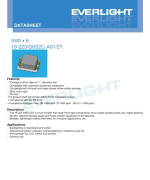
5. Mechanical and Package Information
The package is a standard SMD (Surface Mount Device) type. The dimension drawing (not reproduced here but referenced in the PDF) provides critical measurements for PCB pad design and component placement. Key takeaways include:
- The LED has a compact footprint suitable for high-density boards.
- Tolerances on most dimensions are ±0.1mm unless otherwise specified.
- The drawing defines the component outline, lead positions, and recommended PCB land pattern.
- Polarity identification is typically marked on the device or implied by the pad design.
6. Soldering and Assembly Guidelines
6.1 Reflow Soldering Profile
A lead-free soldering temperature profile is specified:
- Pre-heating: 150~200°C for 60~120 seconds.
- Time Above Liquidus (217°C): 60~150 seconds.
- Peak Temperature: Maximum 260°C.
- Time at Peak: Maximum 10 seconds.
- Heating Rate: Maximum 6°C/sec.
- Time Above 255°C: Maximum 30 seconds.
- Cooling Rate: Maximum 3°C/sec.
Critical Note: Reflow soldering should not be performed more than two times on the same device.
6.2 Hand Soldering
If hand soldering is unavoidable:
- Iron tip temperature must be less than 350°C.
- Contact time per terminal must be less than 3 seconds.
- Soldering iron power should be less than 25W.
- Allow an interval of more than 2 seconds between soldering each terminal.
- Use a double-head soldering iron for any repair work to avoid thermal stress.
6.3 Storage and Moisture Sensitivity
The components are packaged in moisture-resistant bags with desiccant.
- Before Use: Do not open the moisture-proof bag until ready for assembly.
- After Opening: Store at ≤30°C and ≤60% RH.
- Floor Life: Use within 168 hours (7 days) after opening. Reseal unused parts in a moisture-proof package.
- Baking: If the storage time is exceeded or desiccant indicates moisture, bake at 60 ±5°C for 24 hours before use.
7. Packaging and Ordering Information
The product is supplied in a format compatible with automated assembly.
- Tape and Reel: Packaged in 8mm wide tape on a 7-inch diameter reel.
- Quantity: 2000 pieces per reel.
- Carrier Tape Dimensions: Detailed drawings specify pocket size and tape advancement pitch.
- Reel Dimensions: Standard reel dimensions are provided for feeder compatibility.
- Label Information: The reel label includes fields for Customer Product Number (CPN), Product Number (P/N), Quantity (QTY), and technical bins for Luminous Intensity (CAT), Chromaticity/Dominant Wavelength (HUE), and Forward Voltage (REF).
8. Application Recommendations
8.1 Typical Application Scenarios
- Backlighting: Dashboard indicators, switch backlighting, flat backlights for LCDs and symbols.
- Telecommunication Equipment: Status indicators and keypad backlighting in telephones and fax machines.
- General Indication: Any application requiring a compact, reliable, colored light source.
8.2 Critical Design Considerations
- Current Limiting: An external series resistor is MANDATORY. The LED's exponential V-I characteristic means a small voltage change causes a large current change, leading to rapid failure without current regulation.
- Thermal Management: While the package is small, power dissipation (max 60mW) and the negative temperature coefficient of light output necessitate consideration of PCB layout for heat dissipation, especially in high ambient temperatures or at high drive currents.
- ESD Protection: Although rated for 2000V HBM, implement standard ESD precautions during handling and assembly.
- Wave Soldering: Not recommended. The device is specified for reflow or careful hand soldering only.
- Board Stress: Avoid mechanical stress on the LED body during soldering or in the final application. Do not warp the PCB after assembly.
9. Technical Comparison and Differentiation
The 19-223 series, with its AlGaInP chip technology (for G6 and S2), offers distinct advantages:
- vs. Older Through-Hole LEDs: The primary advantage is the dramatic reduction in size and weight, enabling modern miniaturized designs. It also eliminates the need for lead bending and manual insertion.
- vs. Other SMD Colors: The Brilliant Yellow Green (G6, ~575nm) and Brilliant Orange (S2, ~611nm) fill specific color points in the visible spectrum. AlGaInP technology typically offers high efficiency and good color saturation in the red, orange, and yellow-green regions.
- Compliance: Its full compliance with Pb-free, RoHS, Halogen-Free, and REACH regulations makes it suitable for global markets with strict environmental requirements.
10. Frequently Asked Questions (Based on Technical Parameters)
10.1 What resistor value should I use with this LED?
Calculate using Ohm's Law: R = (Vsupply - Vf_LED) / If. For a 5V supply and typical Vf=2.0V at If=20mA: R = (5V - 2.0V) / 0.020A = 150 Ω. Use the maximum Vf (2.4V) to ensure minimum current is safe: R_min = (5V - 2.4V) / 0.020A = 130 Ω. A standard 150 Ω resistor is a good starting point. Always consider power rating of the resistor: P = I^2 * R = (0.02)^2 * 150 = 0.06W, so a 1/8W (0.125W) resistor is sufficient.
10.2 Can I drive it with a 3.3V supply?
Yes. Recalculating: R = (3.3V - 2.0V) / 0.020A = 65 Ω. Check with max Vf: (3.3V - 2.4V) / 0.020A = 45 Ω. A 68 Ω resistor would be appropriate. Ensure the supply can provide the required current.
10.3 Why is the storage and baking process so important?
SMD packages can absorb moisture from the atmosphere. During the high-temperature reflow soldering process, this trapped moisture can rapidly turn to steam, causing internal delamination, cracking, or "popcorning" of the plastic package, leading to immediate or latent failure. The prescribed storage and baking procedures prevent this failure mode.
10.4 What is the difference between Peak Wavelength and Dominant Wavelength?
Peak Wavelength (λp) is the wavelength at which the emission spectrum has its maximum intensity. Dominant Wavelength (λd) is the single wavelength of monochromatic light that would match the perceived color of the LED when combined with a specified white reference source. λd is more closely related to the human eye's perception of color, while λp is a physical measurement of the spectrum.
11. Design and Usage Case Study
Scenario: Designing a multi-indicator status panel for a portable medical device.
Requirements: Compact size, low power consumption, clear color differentiation for "Ready" (Green) and "Alert" (Orange), capable of operating in an extended temperature range, and compliant with medical equipment regulations.
Solution Implementation:
- Component Selection: The 19-223 series is chosen. The G6 (Yellow-Green) serves as the "Ready" indicator, and the S2 (Orange) serves as the "Alert" indicator. Their wide 130-degree viewing angle ensures visibility from various angles.
- Circuit Design: A 3.3V system voltage is used. Current-limiting resistors are calculated as per FAQ 10.2 (e.g., 68Ω). The LEDs are driven via GPIO pins of a microcontroller, allowing software-controlled blinking patterns for enhanced alert status.
- PCB Layout: The compact SMD footprint allows multiple status LEDs to be placed in a small area on the front panel PCB. Thermal relief pads are used in the solder connections to facilitate soldering, but a small amount of copper is kept connected to aid in heat dissipation.
- Assembly Process: The LEDs, delivered on tape-and-reel, are loaded into a pick-and-place machine. The entire board undergoes a single reflow pass using the specified lead-free profile, ensuring all components, including the LEDs, are soldered simultaneously and reliably.
- Result: A robust, reliable, and compact indicator system meeting all initial requirements, leveraging the small size, specified performance, and compliance certifications of the 19-223 LEDs.
12. Technology Principle Introduction
The 19-223 LEDs utilize AlGaInP (Aluminum Gallium Indium Phosphide) semiconductor material for the light-emitting chip. This material system is particularly efficient for producing light in the red, orange, amber, and yellow-green regions of the spectrum (roughly 560nm to 650nm).
Working Principle: When a forward voltage is applied across the LED's p-n junction, electrons and holes are injected into the active region. Their recombination releases energy in the form of photons (light). The specific wavelength (color) of the emitted light is determined by the bandgap energy of the AlGaInP semiconductor, which is engineered by precisely controlling the ratios of Aluminum, Gallium, Indium, and Phosphorus during crystal growth. The "water clear" resin lens allows the intrinsic colored light from the chip to be emitted without significant filtering or wavelength conversion.
13. Industry Trends and Developments
The market for SMD LEDs like the 19-223 series continues to evolve. Key trends influencing this product segment include:
- Increased Miniaturization: Demand for even smaller package sizes (e.g., 0402, 0201 metric) continues to grow for ultra-compact devices.
- Higher Efficiency: Ongoing improvements in epitaxial growth and chip design lead to higher luminous efficacy (more light output per unit of electrical input), reducing power consumption for a given brightness.
- Enhanced Reliability and Robustness: Improvements in package materials and construction aim to increase moisture resistance, thermal cycling performance, and overall longevity, especially for automotive and industrial applications.
- Integration: A trend towards integrating multiple LED chips (RGB, or multiple monochrome) into a single package, or combining LEDs with control ICs (like constant current drivers) to form smarter, simpler-to-use light modules.
- Stringent Compliance: Environmental and safety regulations (RoHS, REACH, Halogen-Free) are becoming more stringent and widespread, making compliance a baseline requirement rather than a differentiator.
The 19-223 series represents a mature, reliable solution that addresses the core needs of miniaturization, automated assembly, and regulatory compliance for a wide range of indicator and backlight applications.
LED Specification Terminology
Complete explanation of LED technical terms
Photoelectric Performance
| Term | Unit/Representation | Simple Explanation | Why Important |
|---|---|---|---|
| Luminous Efficacy | lm/W (lumens per watt) | Light output per watt of electricity, higher means more energy efficient. | Directly determines energy efficiency grade and electricity cost. |
| Luminous Flux | lm (lumens) | Total light emitted by source, commonly called "brightness". | Determines if the light is bright enough. |
| Viewing Angle | ° (degrees), e.g., 120° | Angle where light intensity drops to half, determines beam width. | Affects illumination range and uniformity. |
| CCT (Color Temperature) | K (Kelvin), e.g., 2700K/6500K | Warmth/coolness of light, lower values yellowish/warm, higher whitish/cool. | Determines lighting atmosphere and suitable scenarios. |
| CRI / Ra | Unitless, 0–100 | Ability to render object colors accurately, Ra≥80 is good. | Affects color authenticity, used in high-demand places like malls, museums. |
| SDCM | MacAdam ellipse steps, e.g., "5-step" | Color consistency metric, smaller steps mean more consistent color. | Ensures uniform color across same batch of LEDs. |
| Dominant Wavelength | nm (nanometers), e.g., 620nm (red) | Wavelength corresponding to color of colored LEDs. | Determines hue of red, yellow, green monochrome LEDs. |
| Spectral Distribution | Wavelength vs intensity curve | Shows intensity distribution across wavelengths. | Affects color rendering and quality. |
Electrical Parameters
| Term | Symbol | Simple Explanation | Design Considerations |
|---|---|---|---|
| Forward Voltage | Vf | Minimum voltage to turn on LED, like "starting threshold". | Driver voltage must be ≥Vf, voltages add up for series LEDs. |
| Forward Current | If | Current value for normal LED operation. | Usually constant current drive, current determines brightness & lifespan. |
| Max Pulse Current | Ifp | Peak current tolerable for short periods, used for dimming or flashing. | Pulse width & duty cycle must be strictly controlled to avoid damage. |
| Reverse Voltage | Vr | Max reverse voltage LED can withstand, beyond may cause breakdown. | Circuit must prevent reverse connection or voltage spikes. |
| Thermal Resistance | Rth (°C/W) | Resistance to heat transfer from chip to solder, lower is better. | High thermal resistance requires stronger heat dissipation. |
| ESD Immunity | V (HBM), e.g., 1000V | Ability to withstand electrostatic discharge, higher means less vulnerable. | Anti-static measures needed in production, especially for sensitive LEDs. |
Thermal Management & Reliability
| Term | Key Metric | Simple Explanation | Impact |
|---|---|---|---|
| Junction Temperature | Tj (°C) | Actual operating temperature inside LED chip. | Every 10°C reduction may double lifespan; too high causes light decay, color shift. |
| Lumen Depreciation | L70 / L80 (hours) | Time for brightness to drop to 70% or 80% of initial. | Directly defines LED "service life". |
| Lumen Maintenance | % (e.g., 70%) | Percentage of brightness retained after time. | Indicates brightness retention over long-term use. |
| Color Shift | Δu′v′ or MacAdam ellipse | Degree of color change during use. | Affects color consistency in lighting scenes. |
| Thermal Aging | Material degradation | Deterioration due to long-term high temperature. | May cause brightness drop, color change, or open-circuit failure. |
Packaging & Materials
| Term | Common Types | Simple Explanation | Features & Applications |
|---|---|---|---|
| Package Type | EMC, PPA, Ceramic | Housing material protecting chip, providing optical/thermal interface. | EMC: good heat resistance, low cost; Ceramic: better heat dissipation, longer life. |
| Chip Structure | Front, Flip Chip | Chip electrode arrangement. | Flip chip: better heat dissipation, higher efficacy, for high-power. |
| Phosphor Coating | YAG, Silicate, Nitride | Covers blue chip, converts some to yellow/red, mixes to white. | Different phosphors affect efficacy, CCT, and CRI. |
| Lens/Optics | Flat, Microlens, TIR | Optical structure on surface controlling light distribution. | Determines viewing angle and light distribution curve. |
Quality Control & Binning
| Term | Binning Content | Simple Explanation | Purpose |
|---|---|---|---|
| Luminous Flux Bin | Code e.g., 2G, 2H | Grouped by brightness, each group has min/max lumen values. | Ensures uniform brightness in same batch. |
| Voltage Bin | Code e.g., 6W, 6X | Grouped by forward voltage range. | Facilitates driver matching, improves system efficiency. |
| Color Bin | 5-step MacAdam ellipse | Grouped by color coordinates, ensuring tight range. | Guarantees color consistency, avoids uneven color within fixture. |
| CCT Bin | 2700K, 3000K etc. | Grouped by CCT, each has corresponding coordinate range. | Meets different scene CCT requirements. |
Testing & Certification
| Term | Standard/Test | Simple Explanation | Significance |
|---|---|---|---|
| LM-80 | Lumen maintenance test | Long-term lighting at constant temperature, recording brightness decay. | Used to estimate LED life (with TM-21). |
| TM-21 | Life estimation standard | Estimates life under actual conditions based on LM-80 data. | Provides scientific life prediction. |
| IESNA | Illuminating Engineering Society | Covers optical, electrical, thermal test methods. | Industry-recognized test basis. |
| RoHS / REACH | Environmental certification | Ensures no harmful substances (lead, mercury). | Market access requirement internationally. |
| ENERGY STAR / DLC | Energy efficiency certification | Energy efficiency and performance certification for lighting. | Used in government procurement, subsidy programs, enhances competitiveness. |