1. Product Overview
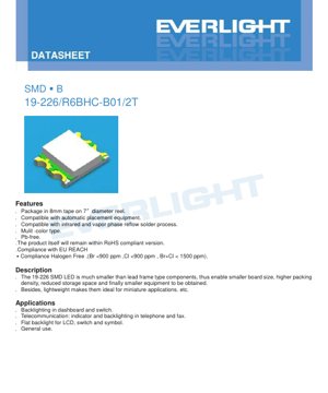
The 19-226 is a compact, surface-mount device (SMD) LED designed for high-density electronic assemblies. Its primary advantage lies in its significantly reduced footprint compared to traditional lead-frame LEDs, enabling smaller printed circuit board (PCB) designs, higher component packing density, and ultimately more compact end-user equipment. The lightweight construction further makes it ideal for miniature and portable applications.
This LED is offered in a multi-color configuration, specifically combining brilliant red (using an R6 AlGaInP chip) and blue (using a BH InGaN chip) emitters within a single, water-clear resin package. It is fully compliant with modern environmental and safety standards, being Pb-free, RoHS compliant, EU REACH compliant, and halogen-free (with Bromine <900 ppm, Chlorine <900 ppm, Br+Cl < 1500 ppm). The device is supplied on 8mm tape mounted on 7-inch diameter reels, making it fully compatible with automated pick-and-place assembly equipment and standard infrared or vapor phase reflow soldering processes.
2. Technical Parameters: In-Depth Objective Interpretation
2.1 Absolute Maximum Ratings
These ratings define the stress limits beyond which permanent damage to the device may occur. Operation under or at these limits is not guaranteed.
- Reverse Voltage (VR): 5V maximum for both chip types. Exceeding this voltage in reverse bias can cause junction breakdown.
- Forward Current (IF): The continuous DC current limit is 25 mA for the R6 (Red) chip and 20 mA for the BH (Blue) chip. This is a critical parameter for determining the series resistor value in the driving circuit.
- Peak Forward Current (IFP): For pulsed operation (1/10 duty cycle @ 1 kHz), the R6 chip can handle up to 60 mA, and the BH chip up to 40 mA. This allows for brief periods of overdrive for higher brightness in multiplexed applications.
- Power Dissipation (Pd): The maximum allowable power dissipation is 60 mW for R6 and 75 mW for BH. This is calculated as IF * VF and is crucial for thermal management.
- Electrostatic Discharge (ESD): The Human Body Model (HBM) rating is 2000V for the R6 chip but only 150V for the more sensitive BH (InGaN) chip. This underscores the necessity for strict ESD protection protocols during handling and assembly of the blue LED.
- Temperature Ranges: Operating temperature (Topr) is -40°C to +85°C. Storage temperature (Tstg) is -40°C to +90°C.
- Soldering Temperature: For reflow soldering, a peak temperature of 260°C for 10 seconds is specified. For hand soldering, the iron tip temperature must not exceed 350°C, and contact time per terminal should be limited to 3 seconds.
2.2 Electro-Optical Characteristics
These parameters are measured at a junction temperature (Tj) of 25°C and define the typical performance of the device.
- Luminous Intensity (Iv): At IF = 20mA, the R6 red LED has a typical intensity of 100 mcd (min. 72 mcd). The BH blue LED has a typical intensity of 80 mcd (min. 45 mcd). A tolerance of ±11% applies.
- Viewing Angle (2θ1/2): The half-intensity angle is typically 120 degrees, providing a wide, diffuse emission pattern suitable for backlighting and indicator applications.
- Wavelength: The R6 chip has a typical peak wavelength (λp) of 632 nm and a dominant wavelength (λd) of 624 nm, placing it in the brilliant red region. The BH chip has a λp of 468 nm and λd of 470 nm, characteristic of a royal blue emission.
- Spectrum Bandwidth (Δλ): The spectral full width at half maximum (FWHM) is 20 nm for R6 and 35 nm for BH.
- Forward Voltage (VF): At IF = 20mA, VF for R6 is typically 2.0V (range 1.7V to 2.4V). For BH, VF is typically 3.3V (range 2.7V to 3.7V). This voltage difference is critical for circuit design when driving both colors, often requiring separate current-limiting resistors or drivers.
- Reverse Current (IR): Maximum IR is 10 µA @ 5V for R6 and 50 µA @ 5V for BH. The datasheet explicitly notes that the device is not designed for reverse operation; this parameter is for test conditions only.
3. Performance Curve Analysis
3.1 Relative Luminous Intensity vs. Forward Current
The curves show that luminous intensity increases with forward current but in a non-linear relationship. For both the R6 and BH chips, the intensity rises steeply at lower currents and tends to saturate at higher currents. Operating significantly above the typical 20mA point yields diminishing returns in light output while increasing heat generation and potentially accelerating lumen depreciation.
3.2 Relative Luminous Intensity vs. Ambient Temperature
This is a critical relationship for reliability. Luminous intensity decreases as ambient temperature increases. The derating curve shows that at the maximum operating temperature of +85°C, the output is significantly reduced compared to the 25°C rating. Designers must account for this thermal derating in applications where high ambient temperatures are expected to ensure sufficient brightness under all conditions.
3.3 Forward Current Derating Curve
This curve dictates the maximum allowable continuous forward current as a function of ambient temperature. To prevent exceeding the maximum junction temperature and power dissipation limits, the forward current must be reduced when operating in high-temperature environments. For example, at an ambient temperature of 85°C, the permissible continuous current is substantially lower than the 25°C maximum rating.
3.4 Forward Voltage vs. Forward Current
The V-I curve demonstrates the diode characteristic. The forward voltage increases logarithmically with current. The typical values provided in the table (2.0V for R6, 3.3V for BH at 20mA) are the most relevant for circuit design calculations.
3.5 Spectrum Distribution
The spectral graphs show the emission profiles. The R6 red LED has a narrower, well-defined peak around 632 nm. The BH blue LED has a broader peak centered around 468-470 nm. These spectra are important for color-sensitive applications.
3.6 Radiation Diagram
The polar plot confirms the near-Lambertian (cosine) emission pattern with a 120-degree viewing angle, indicating even, wide-angle light distribution.
4. Mechanical and Package Information
4.1 Package Dimensions
The SMD package has nominal dimensions of 2.0mm (L) x 1.25mm (W) x 0.8mm (H). The tolerance for unspecified dimensions is ±0.1mm. The drawing details the cathode identification mark, recommended solder pad layout (1.4mm x 1.15mm with a 0.7mm gap), and the component's outline. Adhering to the recommended land pattern is essential for reliable soldering and mechanical stability.
4.2 Polarity Identification
The package features a visual indicator (typically a notch or a green mark on the tape) to identify the cathode. Correct polarity orientation during assembly is mandatory for the device to function.
5. Soldering and Assembly Guidelines
5.1 Reflow Soldering Profile
The datasheet specifies a lead-free reflow profile with a peak temperature of 260°C for 10 seconds. The profile should include preheat, soak, reflow, and cooling zones to minimize thermal shock. Reflow soldering should not be performed more than two times to prevent excessive thermal stress on the LED package and wire bonds.
5.2 Hand Soldering
If hand soldering is unavoidable, extreme care must be taken. The soldering iron tip temperature must be below 350°C, and contact time with each terminal must not exceed 3 seconds. A low-power iron (<25W) is recommended. A two-second interval should be left between soldering each terminal. The datasheet warns that damage often occurs during hand soldering.
5.3 Storage and Moisture Sensitivity
The LEDs are packaged in a moisture-resistant barrier bag with desiccant. The bag must not be opened until the components are ready for use. After opening, unused LEDs should be stored at ≤30°C and ≤60% Relative Humidity. The \"floor life\" after bag opening is 168 hours (7 days). If this time is exceeded or if the desiccant indicator has changed color, a baking treatment at 60°C ±5°C for 24 hours is required before reflow to prevent \"popcorning\" (package cracking due to vapor pressure).
5.4 Precautions for Use
- Over-current Protection: An external current-limiting resistor is mandatory. LEDs are current-driven devices; a small change in forward voltage can cause a large change in current, leading to immediate failure.
- Stress Avoidance: Do not apply mechanical stress to the LED body during heating (soldering) or by warping the PCB after assembly.
- Repairing: Repair after soldering is strongly discouraged. If absolutely necessary, a double-head soldering iron must be used to simultaneously heat both terminals and lift the component without twisting. The impact on LED characteristics must be evaluated beforehand.
6. Packaging and Ordering Information
6.1 Tape and Reel Specifications
The components are supplied in embossed carrier tape with dimensions: pocket pitch 8mm, tape width 12mm. Each reel contains 2000 pieces. The reel dimensions are: 7-inch diameter, 13mm hub diameter, and 50mm reel width.
6.2 Label Explanation
The packaging label includes several codes: Customer's Product Number (CPN), Product Number (P/N), Packing Quantity (QTY), Luminous Intensity Rank (CAT), Chromaticity/Dominant Wavelength Rank (HUE), Forward Voltage Rank (REF), and Lot Number (LOT No). This binning information allows for selection of LEDs with tighter performance parameters if required by the application.
7. Application Suggestions
7.1 Typical Application Scenarios
- Backlighting: Ideal for backlighting dashboards, switches, keypads, and symbols due to its wide viewing angle and compact size.
- Telecommunication Equipment: Status indicators and backlighting for phones, fax machines, and networking hardware.
- LCD Flat Backlighting: Can be used in arrays to provide edge-lighting for small LCD panels.
- General Indicator Use: Status lights, power indicators, and decorative lighting in consumer electronics, appliances, and industrial controls.
7.2 Design Considerations
- Drive Circuit: Always use a series resistor. Calculate resistor value using R = (Vsupply - VF) / IF. Use separate calculations for the red and blue LEDs due to their different VF.
- Thermal Management: Ensure the PCB has adequate thermal relief, especially if driving the LEDs near their maximum current ratings or in high ambient temperatures. Avoid placing heat-generating components nearby.
- ESD Protection: Implement ESD protection on input lines and ensure a grounded work environment during handling, particularly for the sensitive blue (BH) chip.
- Optical Design: The water-clear lens provides a wide viewing angle. For more directed light, external lenses or light guides may be necessary.
8. Technical Comparison and Differentiation
The 19-226's key differentiators in its class are its multi-color capability in a single package and its comprehensive environmental compliance (Pb-free, Halogen-Free, RoHS, REACH). The combination of a high-efficiency AlGaInP red chip and a standard InGaN blue chip in one miniature SMD package offers design flexibility for bi-color indicators without increasing the board footprint. Its compatibility with automatic placement and standard reflow processes aligns with modern, high-volume manufacturing requirements, providing a cost-effective solution for mass-produced electronics.
9. Frequently Asked Questions (Based on Technical Parameters)
Q1: Can I drive the red and blue LEDs from the same power supply and resistor?
A: Not optimally. Due to the significant difference in typical forward voltage (2.0V vs. 3.3V), using a common resistor would result in vastly different currents through each LED, causing one to be dim and the other potentially over-driven. Separate current-limiting circuits are recommended.
Q2: Why is the ESD rating for the blue LED so much lower than for the red?
A: The BH blue LED uses an InGaN semiconductor material, which generally has a more sensitive junction and thinner active layers compared to the AlGaInP material of the R6 red LED, making it more susceptible to electrostatic discharge damage.
Q3: What happens if I exceed the 7-day \"floor life\" after opening the moisture barrier bag?
A: The LED package can absorb moisture from the air. During subsequent reflow soldering, this moisture can rapidly turn to steam, causing internal delamination or cracking (\"popcorning\"). To prevent this, a 24-hour bake at 60°C is required to drive out the moisture before soldering.
Q4: How do I interpret the luminous intensity \"rank\" (CAT) on the label?
A: The rank indicates which pre-defined brightness bin the LED falls into. This allows manufacturers to select LEDs with a guaranteed minimum brightness for consistency in their products, though the specific binning boundaries are not provided in this public datasheet.
10. Practical Use Case Example
Scenario: Designing a Bi-Color Status Indicator for a Consumer Router.
The device needs a single LED to show power (steady blue) and network activity (blinking red). The 19-226 is an ideal choice. The design would involve two separate driver circuits (e.g., microcontroller GPIO pins), each with its own series resistor calculated for 20mA drive current. For a 5V supply: Rblue = (5V - 3.3V) / 0.020A = 85 Ohms (use 82Ω or 100Ω standard value). Rred = (5V - 2.0V) / 0.020A = 150 Ohms (use 150Ω). The compact size allows it to fit next to the RJ45 port. The wide 120-degree viewing angle ensures the status is visible from various angles. Strict ESD handling procedures would be enforced during assembly due to the sensitive blue chip.
11. Operating Principle Introduction
Light Emitting Diodes (LEDs) are semiconductor devices that emit light through electroluminescence. When a forward voltage is applied across the p-n junction, electrons from the n-type region recombine with holes from the p-type region in the active layer. This recombination process releases energy in the form of photons (light). The specific wavelength (color) of the emitted light is determined by the bandgap energy of the semiconductor material used. The R6 chip uses an Aluminum Gallium Indium Phosphide (AlGaInP) structure, which is efficient for producing red and amber light. The BH chip uses Indium Gallium Nitride (InGaN), which is commonly used for blue, green, and white LEDs. The water-clear epoxy resin package serves to protect the semiconductor chip, provide mechanical support for the bonding wires, and acts as a primary lens to shape the light output.
12. Technology Trends and Context
The 19-226 represents a mature product in the SMD LED market. Current industry trends focus on several key areas beyond the specifications of this device: Increased Efficiency (lm/W): Newer chip designs and materials continue to push luminous efficacy higher. Higher Color Rendering Index (CRI): Especially for white LEDs and lighting applications. Miniaturization: Even smaller package sizes (e.g., 01005, micro-LEDs) for ultra-high-density displays. Integrated Drivers: LEDs with built-in constant-current drivers or control circuitry (smart LEDs). Improved Thermal Performance: Packages designed to better extract heat, allowing for higher drive currents and longer lifespan. Expanded Wavelengths: Development of more efficient deep-UV and infrared LEDs for sensing and sterilization applications. While the 19-226 may not incorporate the latest advancements in peak efficiency, its combination of reliable performance, dual-color output, robust packaging, and full compliance with global environmental standards ensures its continued relevance in a wide array of cost-sensitive, high-volume electronic indicator and backlight applications.
LED Specification Terminology
Complete explanation of LED technical terms
Photoelectric Performance
| Term | Unit/Representation | Simple Explanation | Why Important |
|---|---|---|---|
| Luminous Efficacy | lm/W (lumens per watt) | Light output per watt of electricity, higher means more energy efficient. | Directly determines energy efficiency grade and electricity cost. |
| Luminous Flux | lm (lumens) | Total light emitted by source, commonly called "brightness". | Determines if the light is bright enough. |
| Viewing Angle | ° (degrees), e.g., 120° | Angle where light intensity drops to half, determines beam width. | Affects illumination range and uniformity. |
| CCT (Color Temperature) | K (Kelvin), e.g., 2700K/6500K | Warmth/coolness of light, lower values yellowish/warm, higher whitish/cool. | Determines lighting atmosphere and suitable scenarios. |
| CRI / Ra | Unitless, 0–100 | Ability to render object colors accurately, Ra≥80 is good. | Affects color authenticity, used in high-demand places like malls, museums. |
| SDCM | MacAdam ellipse steps, e.g., "5-step" | Color consistency metric, smaller steps mean more consistent color. | Ensures uniform color across same batch of LEDs. |
| Dominant Wavelength | nm (nanometers), e.g., 620nm (red) | Wavelength corresponding to color of colored LEDs. | Determines hue of red, yellow, green monochrome LEDs. |
| Spectral Distribution | Wavelength vs intensity curve | Shows intensity distribution across wavelengths. | Affects color rendering and quality. |
Electrical Parameters
| Term | Symbol | Simple Explanation | Design Considerations |
|---|---|---|---|
| Forward Voltage | Vf | Minimum voltage to turn on LED, like "starting threshold". | Driver voltage must be ≥Vf, voltages add up for series LEDs. |
| Forward Current | If | Current value for normal LED operation. | Usually constant current drive, current determines brightness & lifespan. |
| Max Pulse Current | Ifp | Peak current tolerable for short periods, used for dimming or flashing. | Pulse width & duty cycle must be strictly controlled to avoid damage. |
| Reverse Voltage | Vr | Max reverse voltage LED can withstand, beyond may cause breakdown. | Circuit must prevent reverse connection or voltage spikes. |
| Thermal Resistance | Rth (°C/W) | Resistance to heat transfer from chip to solder, lower is better. | High thermal resistance requires stronger heat dissipation. |
| ESD Immunity | V (HBM), e.g., 1000V | Ability to withstand electrostatic discharge, higher means less vulnerable. | Anti-static measures needed in production, especially for sensitive LEDs. |
Thermal Management & Reliability
| Term | Key Metric | Simple Explanation | Impact |
|---|---|---|---|
| Junction Temperature | Tj (°C) | Actual operating temperature inside LED chip. | Every 10°C reduction may double lifespan; too high causes light decay, color shift. |
| Lumen Depreciation | L70 / L80 (hours) | Time for brightness to drop to 70% or 80% of initial. | Directly defines LED "service life". |
| Lumen Maintenance | % (e.g., 70%) | Percentage of brightness retained after time. | Indicates brightness retention over long-term use. |
| Color Shift | Δu′v′ or MacAdam ellipse | Degree of color change during use. | Affects color consistency in lighting scenes. |
| Thermal Aging | Material degradation | Deterioration due to long-term high temperature. | May cause brightness drop, color change, or open-circuit failure. |
Packaging & Materials
| Term | Common Types | Simple Explanation | Features & Applications |
|---|---|---|---|
| Package Type | EMC, PPA, Ceramic | Housing material protecting chip, providing optical/thermal interface. | EMC: good heat resistance, low cost; Ceramic: better heat dissipation, longer life. |
| Chip Structure | Front, Flip Chip | Chip electrode arrangement. | Flip chip: better heat dissipation, higher efficacy, for high-power. |
| Phosphor Coating | YAG, Silicate, Nitride | Covers blue chip, converts some to yellow/red, mixes to white. | Different phosphors affect efficacy, CCT, and CRI. |
| Lens/Optics | Flat, Microlens, TIR | Optical structure on surface controlling light distribution. | Determines viewing angle and light distribution curve. |
Quality Control & Binning
| Term | Binning Content | Simple Explanation | Purpose |
|---|---|---|---|
| Luminous Flux Bin | Code e.g., 2G, 2H | Grouped by brightness, each group has min/max lumen values. | Ensures uniform brightness in same batch. |
| Voltage Bin | Code e.g., 6W, 6X | Grouped by forward voltage range. | Facilitates driver matching, improves system efficiency. |
| Color Bin | 5-step MacAdam ellipse | Grouped by color coordinates, ensuring tight range. | Guarantees color consistency, avoids uneven color within fixture. |
| CCT Bin | 2700K, 3000K etc. | Grouped by CCT, each has corresponding coordinate range. | Meets different scene CCT requirements. |
Testing & Certification
| Term | Standard/Test | Simple Explanation | Significance |
|---|---|---|---|
| LM-80 | Lumen maintenance test | Long-term lighting at constant temperature, recording brightness decay. | Used to estimate LED life (with TM-21). |
| TM-21 | Life estimation standard | Estimates life under actual conditions based on LM-80 data. | Provides scientific life prediction. |
| IESNA | Illuminating Engineering Society | Covers optical, electrical, thermal test methods. | Industry-recognized test basis. |
| RoHS / REACH | Environmental certification | Ensures no harmful substances (lead, mercury). | Market access requirement internationally. |
| ENERGY STAR / DLC | Energy efficiency certification | Energy efficiency and performance certification for lighting. | Used in government procurement, subsidy programs, enhances competitiveness. |