Table of Contents
- 1. Product Overview
- 2. Technical Specifications Deep Dive
- 2.1 Absolute Maximum Ratings
- 2.2 Recommended Operating Conditions
- 2.3 Electro-Optical Characteristics
- 3. Binning System Explanation
- 3.1 Luminous Intensity Binning
- 3.2 Dominant Wavelength Binning
- 4. Performance and Timing Analysis
- 4.1 Timing Waveform and Communication Protocol
- 4.2 Application Circuit
- 5. Mechanical and Package Information
- 5.1 Package Dimensions
- 5.2 Packaging Specifications
- 6. Soldering, Assembly, and Usage Guidelines
- 6.1 Soldering Process Compatibility
- 6.2 Critical Usage Precautions
- 7. Application Suggestions and Design Considerations
- 7.1 Typical Application Scenarios
- 7.2 Design Considerations
- 8. Technical Comparison and Differentiation
- 9. Frequently Asked Questions (Based on Technical Parameters)
- 10. Operational Principles
1. Product Overview
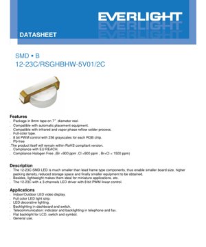
The 12-23C is a compact, surface-mount device (SMD) integrating three individual LED chips (Red, Green, Blue) with a dedicated 3-channel constant current driver IC. This integration enables full-color capability with precise digital control in a single, miniature package. Its primary advantage lies in enabling high-density PCB designs for applications requiring vibrant, dynamically controlled color lighting without the complexity of external driver circuits.
The core functionality is driven by an integrated circuit that accepts a serial digital data signal. This signal contains 24 bits of data (8 bits per color channel), allowing for 256 distinct grayscale levels per color, resulting in over 16 million possible color combinations. The device is packaged on 8mm tape and supplied on 7-inch diameter reels, making it fully compatible with high-speed automated pick-and-place assembly equipment.
2. Technical Specifications Deep Dive
2.1 Absolute Maximum Ratings
These ratings define the limits beyond which permanent damage to the device may occur. Operation should always remain within these boundaries.
- Supply Voltage (VDD): +3.8V to +5.5V. This is the voltage range for the internal driver IC's logic and control circuitry.
- Output Voltage (VOUT): 17V maximum. This rating pertains to the voltage withstand capability of the internal driver's output transistors connected to the LED anodes.
- Input Voltage (VIN): -0.5V to VDD+0.5V. Applies to the digital input pins (DIN). Exceeding this can damage the input protection structures.
- Electrostatic Discharge (ESD): 2000V (Human Body Model). Indicates a moderate level of ESD protection; proper handling procedures are still recommended.
- Operating Temperature (Topr): -20°C to +70°C. The ambient temperature range for reliable operation.
- Storage Temperature (Tstg): -40°C to +90°C.
- Soldering Temperature: The device is rated for reflow soldering with a peak temperature of 260°C for 10 seconds, or hand soldering at 350°C for 3 seconds.
2.2 Recommended Operating Conditions
These are the conditions for optimal and guaranteed performance.
- Supply Voltage (VDD): 5.0V (Typical). The device is designed for a 5V logic supply.
- Input Logic Levels:
- High-Level Input Voltage (VIH): Minimum 0.7*VDD. A signal must be above this level to be recognized as a logic '1'.
- Low-Level Input Voltage (VIL): Maximum 0.3*VDD. A signal must be below this level to be recognized as a logic '0'.
- Propagation Delay (TPLZ): Maximum 300 ns. This is the time delay for a data signal to propagate from the DIN pin to the DOUT pin, crucial for determining maximum data transmission speed in daisy-chained configurations.
- Output Fall Time (TTHZ): Maximum 20 µs for the R/G/B output channels. This affects the PWM switching characteristics.
- Input Capacitance (CI): Maximum 15 pF. The capacitive load presented by the DIN pin.
2.3 Electro-Optical Characteristics
Measured at a forward current (IF) of 5mA per color chip and an ambient temperature (Ta) of 25°C.
- Luminous Intensity (Iv):
- Red (RS): Typical values range from 22.5 mcd to 72.0 mcd, depending on the specific bin.
- Green (GH): Typical values range from 45.0 mcd to 140.0 mcd.
- Blue (BH): Typical values range from 18.0 mcd to 57.0 mcd.
- Viewing Angle (2θ1/2): 130 degrees (Typical). This wide viewing angle is characteristic of the white diffused resin lens.
- Peak Wavelength (λp):
- Red: 632 nm
- Green: 518 nm
- Blue: 468 nm
- Dominant Wavelength (λd): The perceived color wavelength.
- Red: 617.5 nm to 629.5 nm
- Green: 525.0 nm to 540.0 nm
- Blue: 464.5 nm to 476.5 nm
- Spectral Bandwidth (Δλ):
- Red: 20 nm
- Green: 35 nm
- Blue: 25 nm
3. Binning System Explanation
The device is sorted into bins based on key optical parameters to ensure color and brightness consistency within a production batch.
3.1 Luminous Intensity Binning
Each color chip is binned separately. The bin code (e.g., M2, N1, P2) defines a minimum and maximum luminous intensity range at IF=5mA. For example, a Red chip in bin P1 has an intensity between 45.0 and 57.0 mcd. The datasheet provides detailed tables for Red (RS), Green (GH), and Blue (BH). A tolerance of ±11% applies to the luminous intensity.
3.2 Dominant Wavelength Binning
Similar to intensity, the dominant wavelength is also binned to control color point. For instance, a Green chip in bin 'Y' has a dominant wavelength between 525.0 nm and 530.0 nm. The datasheet provides tables for all three colors. A tolerance of ±1nm is specified for the dominant wavelength.
4. Performance and Timing Analysis
4.1 Timing Waveform and Communication Protocol
The device uses a single-wire, serial communication protocol. Data is clocked in on the rising edge of the signal. The protocol defines two logic levels: '0' code and '1' code, each with specific high-time (T1H, T0H) and low-time (T1L, T0L) requirements.
- T0H: 300 ns ±80 ns (0 code, high-level time).
- T0L: 900 ns ±80 ns (0 code, low-level time).
- T1H: 900 ns ±80 ns (1 code, high-level time).
- T1L: 300 ns ±80 ns (1 code, low-level time).
- RES (Reset Time): >50 µs. A low signal on DIN lasting longer than this resets the internal shift register and latches the data to the output.
Twenty-four bits of data are transmitted sequentially: typically 8 bits for Green, 8 bits for Red, and 8 bits for Blue (GRB order). The data for multiple devices can be daisy-chained from the DOUT of one device to the DIN of the next.
4.2 Application Circuit
For a 5V system, the datasheet recommends placing a 0.1 µF decoupling capacitor between the AVDD (power) and GND pins, positioned as close as possible to the device to minimize noise and ensure stable operation. The internal driver is a constant current type; however, the absolute maximum ratings indicate that external current-limiting resistors may be required depending on the applied drain voltage (the voltage at the LED anode, which is higher than VDD) to prevent over-current conditions. The specific resistor values are determined by the target LED current and the forward voltage of the LED chips at that current.
5. Mechanical and Package Information
5.1 Package Dimensions
The device has a compact SMD footprint. The dimensional drawing shows a body size and lead configuration. All unspecified tolerances are ±0.1mm. The pinout is as follows:
- DIN: Data Input for the serial control signal.
- GND: Common ground for both data and power.
- DOUT: Data Output for daisy-chaining to the next device.
- AVDD: Power supply input, connect to +5V.
5.2 Packaging Specifications
The device is supplied in moisture-resistant packaging.
- Carrier Tape: 8mm wide tape on a 7-inch diameter reel. Each reel contains 2000 pieces.
- Moisture Sensitivity: The components are moisture-sensitive (likely MSL 3 or similar). Precautions include:
- Storage before bag opening: ≤30°C / ≤90% RH.
- Floor life after bag opening: 24 hours at ≤30°C / ≤60% RH.
- Unused parts must be re-bagged with desiccant if exceeding floor life.
- Baking is required if the desiccant indicator shows saturation or storage time is exceeded.
- Reel and Tape Dimensions: Detailed drawings are provided for the reel, carrier tape pockets, and cover tape.
- Label Information: The reel label includes fields for Customer Part Number (CPN), Product Number (P/N), Quantity (QTY), and the specific Binning codes for Luminous Intensity (CAT), Wavelength (HUE), and Forward Voltage (REF).
6. Soldering, Assembly, and Usage Guidelines
6.1 Soldering Process Compatibility
The 12-23C is compatible with both infrared and vapor phase reflow soldering processes, adhering to the profile with a peak temperature of 260°C for up to 10 seconds. It is also rated for hand soldering at 350°C for 3 seconds. The product is Pb-free and compliant with RoHS, EU REACH, and halogen-free standards (Br <900ppm, Cl <900ppm, Br+Cl <1500ppm).
6.2 Critical Usage Precautions
- Over-Current Protection: It is mandatory to use external current-limiting resistors in series with each LED color channel. The LED forward voltage has a negative temperature coefficient, meaning current increases as temperature rises. Without resistors, even a small increase in supply voltage or junction temperature can lead to thermal runaway and device failure.
- ESD Precautions: While rated for 2000V HBM, standard ESD handling procedures should be followed during assembly and handling.
- Thermal Management: The maximum operating junction temperature is limited by the driver IC and LED chips. Adequate PCB copper area (thermal relief) should be used for the GND pad to dissipate heat, especially when driving the LEDs at higher currents.
7. Application Suggestions and Design Considerations
7.1 Typical Application Scenarios
- Indoor/Outdoor LED Video Displays: Ideal for fine-pitch displays due to small size, integrated driver, and daisy-chain capability.
- Full-Color LED Light Strips: Enables addressable, programmable RGB lighting strips.
- LED Decorative Lighting: Architectural lighting, signage, and mood lighting.
- Backlighting: For instrument panels, switches, LCDs, and symbols where dynamic color is desired.
- Telecommunication Equipment: Status indicators and keypad backlighting.
7.2 Design Considerations
- Power Supply: Use a clean, regulated 5V supply. The 0.1µF decoupling capacitor is critical for noise immunity.
- Data Line Integrity: For long daisy chains or high-speed data, consider the trace impedance and potential need for a series resistor near the driver output to reduce ringing.
- Current Setting: Calculate the external resistor value (Rext) using the formula: Rext = (Vdrain - Vf_led - Vds_sat) / Iled_target. Where Vdrain is the anode supply voltage (<17V), Vf_led is the LED forward voltage at target current, Vds_sat is the driver output transistor saturation voltage (from driver IC datasheet, if available), and Iled_target is the desired LED current (e.g., 5mA for spec measurements).
- Color Consistency: For applications requiring uniform color, specify tight binning codes (CAT and HUE) from the supplier.
8. Technical Comparison and Differentiation
The 12-23C's primary differentiation is the integration of the LED chips and the driver IC. Compared to using discrete LEDs with a separate driver IC, this solution offers:
- Reduced Component Count: Fewer parts to place and solder.
- Smaller Footprint: Enables higher density designs.
- Simplified PCB Layout: No need to route high-current driver traces from a central IC to distant LEDs.
- Digital Control Simplicity: A single data line controls color and brightness, reducing microcontroller pin count and software complexity compared to analog PWM control of separate channels.
- Daisy-Chaining: Simplifies wiring for linear arrays like light strips.
9. Frequently Asked Questions (Based on Technical Parameters)
Q: What is the maximum data rate I can use?
A: The limiting factor is the propagation delay (300ns max) and the timing requirements for T0H/T1H. A conservative estimate for the data period is about 1.2µs (T0H+T0L for a '0'), which translates to a data rate of approximately 833 kHz. However, the reset time (50µs) between frames will reduce the effective refresh rate.
Q: Can I drive the LEDs at more than 5mA?
A: The datasheet only specifies characteristics at 5mA. Driving at higher currents will increase luminous output but also increase power dissipation, junction temperature, and may reduce lifetime. The maximum current is limited by the driver IC's capability and the LED's own ratings, which are not fully detailed here. Derating and thermal analysis are essential.
Q: How do I calculate the external resistor value?
A: As described in section 7.2. You need the LED Vf curve (often estimated from typical values in the datasheet) and the voltage of your anode supply (Vdrain). A common Vdrain is 12V. Example for Red LED at 5mA: If Vf_red ≈ 2.0V and Vds_sat ≈ 0.6V, then R = (12V - 2.0V - 0.6V) / 0.005A = 1880 Ω. Use the nearest standard value.
Q: What is the difference between peak wavelength and dominant wavelength?
A: Peak wavelength (λp) is the wavelength at the highest point in the LED's spectral power distribution curve. Dominant wavelength (λd) is the wavelength of a pure monochromatic light that matches the perceived color of the LED. λd is more relevant for color mixing and display applications.
10. Operational Principles
The device operates on a simple principle. An internal shift register receives serial data on the DIN pin. This data is clocked in bit by bit based on the timing of the input signal. After 24 bits are received, a low signal on DIN lasting longer than the RES time (50µs) latches this data into a holding register. The holding register's value controls three separate pulse-width modulation (PWM) generators, one for each color channel (Red, Green, Blue). Each 8-bit value (0-255) sets the duty cycle of its corresponding PWM generator, thereby controlling the average current, and thus the brightness, of each LED chip over time. The human eye integrates this rapid blinking, perceiving it as a steady color with adjustable intensity. The DOUT pin provides a buffered copy of the input data stream, allowing seamless daisy-chaining to an unlimited number of subsequent devices.
LED Specification Terminology
Complete explanation of LED technical terms
Photoelectric Performance
| Term | Unit/Representation | Simple Explanation | Why Important |
|---|---|---|---|
| Luminous Efficacy | lm/W (lumens per watt) | Light output per watt of electricity, higher means more energy efficient. | Directly determines energy efficiency grade and electricity cost. |
| Luminous Flux | lm (lumens) | Total light emitted by source, commonly called "brightness". | Determines if the light is bright enough. |
| Viewing Angle | ° (degrees), e.g., 120° | Angle where light intensity drops to half, determines beam width. | Affects illumination range and uniformity. |
| CCT (Color Temperature) | K (Kelvin), e.g., 2700K/6500K | Warmth/coolness of light, lower values yellowish/warm, higher whitish/cool. | Determines lighting atmosphere and suitable scenarios. |
| CRI / Ra | Unitless, 0–100 | Ability to render object colors accurately, Ra≥80 is good. | Affects color authenticity, used in high-demand places like malls, museums. |
| SDCM | MacAdam ellipse steps, e.g., "5-step" | Color consistency metric, smaller steps mean more consistent color. | Ensures uniform color across same batch of LEDs. |
| Dominant Wavelength | nm (nanometers), e.g., 620nm (red) | Wavelength corresponding to color of colored LEDs. | Determines hue of red, yellow, green monochrome LEDs. |
| Spectral Distribution | Wavelength vs intensity curve | Shows intensity distribution across wavelengths. | Affects color rendering and quality. |
Electrical Parameters
| Term | Symbol | Simple Explanation | Design Considerations |
|---|---|---|---|
| Forward Voltage | Vf | Minimum voltage to turn on LED, like "starting threshold". | Driver voltage must be ≥Vf, voltages add up for series LEDs. |
| Forward Current | If | Current value for normal LED operation. | Usually constant current drive, current determines brightness & lifespan. |
| Max Pulse Current | Ifp | Peak current tolerable for short periods, used for dimming or flashing. | Pulse width & duty cycle must be strictly controlled to avoid damage. |
| Reverse Voltage | Vr | Max reverse voltage LED can withstand, beyond may cause breakdown. | Circuit must prevent reverse connection or voltage spikes. |
| Thermal Resistance | Rth (°C/W) | Resistance to heat transfer from chip to solder, lower is better. | High thermal resistance requires stronger heat dissipation. |
| ESD Immunity | V (HBM), e.g., 1000V | Ability to withstand electrostatic discharge, higher means less vulnerable. | Anti-static measures needed in production, especially for sensitive LEDs. |
Thermal Management & Reliability
| Term | Key Metric | Simple Explanation | Impact |
|---|---|---|---|
| Junction Temperature | Tj (°C) | Actual operating temperature inside LED chip. | Every 10°C reduction may double lifespan; too high causes light decay, color shift. |
| Lumen Depreciation | L70 / L80 (hours) | Time for brightness to drop to 70% or 80% of initial. | Directly defines LED "service life". |
| Lumen Maintenance | % (e.g., 70%) | Percentage of brightness retained after time. | Indicates brightness retention over long-term use. |
| Color Shift | Δu′v′ or MacAdam ellipse | Degree of color change during use. | Affects color consistency in lighting scenes. |
| Thermal Aging | Material degradation | Deterioration due to long-term high temperature. | May cause brightness drop, color change, or open-circuit failure. |
Packaging & Materials
| Term | Common Types | Simple Explanation | Features & Applications |
|---|---|---|---|
| Package Type | EMC, PPA, Ceramic | Housing material protecting chip, providing optical/thermal interface. | EMC: good heat resistance, low cost; Ceramic: better heat dissipation, longer life. |
| Chip Structure | Front, Flip Chip | Chip electrode arrangement. | Flip chip: better heat dissipation, higher efficacy, for high-power. |
| Phosphor Coating | YAG, Silicate, Nitride | Covers blue chip, converts some to yellow/red, mixes to white. | Different phosphors affect efficacy, CCT, and CRI. |
| Lens/Optics | Flat, Microlens, TIR | Optical structure on surface controlling light distribution. | Determines viewing angle and light distribution curve. |
Quality Control & Binning
| Term | Binning Content | Simple Explanation | Purpose |
|---|---|---|---|
| Luminous Flux Bin | Code e.g., 2G, 2H | Grouped by brightness, each group has min/max lumen values. | Ensures uniform brightness in same batch. |
| Voltage Bin | Code e.g., 6W, 6X | Grouped by forward voltage range. | Facilitates driver matching, improves system efficiency. |
| Color Bin | 5-step MacAdam ellipse | Grouped by color coordinates, ensuring tight range. | Guarantees color consistency, avoids uneven color within fixture. |
| CCT Bin | 2700K, 3000K etc. | Grouped by CCT, each has corresponding coordinate range. | Meets different scene CCT requirements. |
Testing & Certification
| Term | Standard/Test | Simple Explanation | Significance |
|---|---|---|---|
| LM-80 | Lumen maintenance test | Long-term lighting at constant temperature, recording brightness decay. | Used to estimate LED life (with TM-21). |
| TM-21 | Life estimation standard | Estimates life under actual conditions based on LM-80 data. | Provides scientific life prediction. |
| IESNA | Illuminating Engineering Society | Covers optical, electrical, thermal test methods. | Industry-recognized test basis. |
| RoHS / REACH | Environmental certification | Ensures no harmful substances (lead, mercury). | Market access requirement internationally. |
| ENERGY STAR / DLC | Energy efficiency certification | Energy efficiency and performance certification for lighting. | Used in government procurement, subsidy programs, enhances competitiveness. |