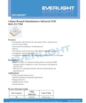
1. Product Overview
The IR42-21C/TR8 is a subminiature, surface-mount infrared emitting diode designed for compact optoelectronic applications. It features a 1.8mm diameter round package molded from water-clear plastic with a spherical top lens, optimizing light output. The device utilizes a Gallium Aluminum Arsenide (GaAlAs) chip material, which is spectrally matched to silicon photodiodes and phototransistors, ensuring efficient detection in sensor systems. Its primary design goals are miniaturization, compatibility with automated assembly processes, and reliable performance in a range of consumer and industrial electronic devices.
1.1 Core Advantages and Target Market
This LED offers several key advantages for designers. Its low forward voltage (typically 1.2V) contributes to energy-efficient operation. The component is fully compliant with lead-free (Pb-free), RoHS, EU REACH, and halogen-free regulations (Br<900ppm, Cl<900ppm, Br+Cl<1500ppm), making it suitable for global markets with strict environmental standards. It is compatible with both infrared and vapor phase reflow soldering processes, facilitating high-volume, automated PCB assembly. The primary target markets include manufacturers of compact infrared sensors, miniature light barriers for automation, floppy disk drives (for legacy or specialized systems), general-purpose optoelectronic switches, and smoke detection systems where an invisible IR source is required.
2. In-Depth Technical Parameter Analysis
The performance of the IR42-21C/TR8 is defined by a set of absolute maximum ratings and electro-optical characteristics measured at a standard ambient temperature (Ta) of 25\u00b0C. Understanding these parameters is critical for reliable circuit design and ensuring the LED operates within its safe operating area (SOA).
2.1 Absolute Maximum Ratings
These ratings define the stress limits beyond which permanent damage to the device may occur. They should never be exceeded, even momentarily. The continuous forward current (IF) is rated at 65 mA. The maximum permissible reverse voltage (VR) is 5 V. The device can operate within an ambient temperature range (Topr) of -25\u00b0C to +85\u00b0C and be stored (Tstg) between -40\u00b0C and +85\u00b0C. The soldering temperature (Tsol) must not exceed 260\u00b0C for a duration of 5 seconds or less during reflow processes. The total power dissipation (Pd) at or below 25\u00b0C free air temperature is 130 mW. Exceeding any of these limits risks catastrophic failure or accelerated degradation.
2.2 Electro-Optical Characteristics
These parameters, typically measured at a forward current (IF) of 20 mA, define the device's functional performance. The radiant intensity (Ie), a measure of optical power emitted per solid angle, has a minimum value of 1.0 mW/sr and a typical value of 3.0 mW/sr. The peak wavelength (\u03bbp) is typically 940 nm, placing it firmly in the near-infrared spectrum, which is ideal for silicon-based detectors. The spectral bandwidth (\u0394\u03bb) is typically 45 nm, defining the range of wavelengths emitted. The forward voltage (VF) has a typical value of 1.2 V and a maximum of 1.5 V at 20 mA. The reverse current (IR) is a maximum of 10 \u00b5A when a 5 V reverse bias is applied. The viewing angle (2\u03b81/2), defined as the full angle at which the radiant intensity drops to half its peak value, is typically 30 degrees, providing a moderately focused beam.
3. Performance Curve Analysis
The datasheet provides several characteristic curves that illustrate how key parameters vary with operating conditions. These graphs are essential for understanding real-world behavior beyond the single-point specifications at 25\u00b0C.
3.1 Forward Current vs. Ambient Temperature
This curve shows the relationship between the permissible continuous forward current and the ambient temperature. As the ambient temperature increases, the maximum allowable forward current decreases linearly. This derating is necessary to prevent the junction temperature from exceeding its limit, which is linked to the power dissipation rating. Designers must use this graph to select an appropriate operating current for their application's maximum expected ambient temperature.
3.2 Spectral Distribution
The spectral distribution curve plots relative radiant intensity against wavelength. It visually confirms the peak wavelength of 940 nm and the approximately 45 nm spectral bandwidth. The curve is asymmetrical, which is typical for LED emission spectra. This information is crucial for applications requiring specific spectral matching with a photodetector's responsivity curve.
3.3 Forward Current vs. Forward Voltage
This IV (Current-Voltage) characteristic curve is non-linear, like all diodes. It shows that a small increase in forward voltage beyond the \"knee\" voltage results in a large, exponential increase in forward current. This underscores the critical importance of using a series current-limiting resistor or a constant-current driver to prevent thermal runaway and destruction of the LED from overcurrent.
3.4 Relative Radiant Intensity vs. Angular Displacement
This polar plot illustrates the spatial emission pattern of the LED. The intensity is normalized to its maximum value at 0 degrees (on-axis). The curve shows how the intensity falls off as the observation angle increases, defining the 30-degree viewing angle where intensity is 50% of the peak. The pattern is generally Lambertian (cosine-like) for this dome-shaped package, which is useful for calculating irradiance at a detector.
4. Mechanical and Packaging Information
4.1 Package Dimensions
The device is housed in a compact, round SMD package with a diameter of 1.8mm. Detailed mechanical drawings in the datasheet provide all critical dimensions, including body height, lead spacing, and lens geometry. All dimensions are in millimeters, with standard tolerances of \u00b10.1mm unless otherwise specified. A suggested pad layout is provided for PCB design, but it is explicitly noted that this is for reference only and should be modified based on individual process requirements and thermal management needs.
4.2 Polarity Identification and Carrier Taping
The package features a flat side or a similar marking to indicate the cathode (negative) lead, which is essential for correct orientation during assembly. For high-volume production, the components are supplied on carrier tape reels. The datasheet includes the carrier tape dimensions, specifying the pocket size, pitch, and reel diameter. A standard reel contains 1000 pieces, which is typical for automated pick-and-place machinery.
5. Soldering and Assembly Guidelines
Proper handling and soldering are vital for reliability. The LED is moisture-sensitive and comes in a moisture barrier bag with a desiccant.
5.1 Storage and Moisture Sensitivity
Before opening the sealed bag, the LEDs must be stored at 30\u00b0C or less and 90% Relative Humidity (RH) or less. The shelf life is one year. After opening the bag, the components should be kept at 30\u00b0C/60%RH or less and must be used within 168 hours (7 days). If the storage time is exceeded or the desiccant indicates moisture ingress, a baking treatment at 60 \u00b1 5\u00b0C for 24 hours is required before use to remove absorbed moisture and prevent \"popcorning\" during reflow soldering.
5.2 Reflow Soldering Parameters
The device is compatible with lead-free (Pb-free) reflow soldering profiles. A specific temperature profile is recommended, typically involving a preheat stage, a soak zone, a peak temperature zone not exceeding 260\u00b0C for a maximum of 5 seconds, and a controlled cooling stage. Reflow soldering should not be performed more than two times. During heating, no mechanical stress should be applied to the LED body or leads, and the PCB should not be warped after soldering.
5.3 Hand Soldering and Rework
If hand soldering is unavoidable, extreme care must be taken. The soldering iron tip temperature should be below 350\u00b0C, and contact time with each terminal should be limited to 3 seconds or less. A low-power iron (25W or less) is recommended. A pause of at least 2 seconds should be observed between soldering each lead. Rework after initial soldering is strongly discouraged. If absolutely necessary, a specialized double-head soldering iron should be used to simultaneously heat both leads and lift the component without stressing the package. The potential for damage during rework is high.
6. Application Suggestions and Design Considerations
6.1 Typical Application Circuits
The most fundamental application circuit is a simple series connection of the LED, a current-limiting resistor, and a voltage source. The resistor value (R) is calculated using Ohm's Law: R = (V_source - VF_LED) / IF. For example, with a 5V source, a VF of 1.2V, and a desired IF of 20mA, R = (5 - 1.2) / 0.02 = 190 Ohms. A 200 Ohm resistor would be a suitable standard value. For more stable operation, especially with a variable supply voltage, a constant current driver circuit is preferred.
6.2 Design Considerations for Infrared Systems
When designing an infrared sensing system, several factors must be considered. Optical alignment between the IR LED and the photodetector is critical, especially with a 30-degree beam. Ambient light rejection is often necessary; this can be achieved by modulating the LED drive current and using a synchronized detector circuit to filter out DC ambient light. The radiant intensity and detector sensitivity must be matched for the required sensing distance. Thermal management should be considered if operating near maximum ratings, as increased junction temperature reduces light output and lifespan.
7. Technical Comparison and Differentiation
Compared to larger through-hole IR LEDs, the primary advantage of the IR42-21C/TR8 is its miniature SMD footprint, enabling smaller, lighter, and more automated PCB designs. Compared to other SMD IR LEDs, its key differentiators are its specific 1.8mm round package size, the 940nm peak wavelength optimized for silicon detectors, and its compliance with the latest environmental regulations (Halogen-Free, REACH). The water-clear lens, as opposed to a tinted or diffused lens, maximizes the transmission of the infrared light, yielding higher radiant intensity for a given electrical input.
8. Frequently Asked Questions (Based on Technical Parameters)
Q: Why is a current-limiting resistor absolutely necessary?
A: The IV curve shows the LED's exponential relationship between voltage and current. A slight increase in supply voltage or a drop in the LED's forward voltage (due to temperature) can cause a massive, uncontrolled surge in current, leading to immediate burnout. The resistor provides a linear, stabilizing impedance.
Q: Can I drive this LED with a 3.3V microcontroller pin directly?
A: Possibly, but not optimally. With a VF of 1.2V, a series resistor would be needed. The current available from a GPIO pin is often limited (e.g., 20-25mA). You must ensure the total current draw, including the resistor calculation (R = (3.3V - 1.2V) / I_desired), does not exceed the GPIO's current sourcing capability. For higher currents or multiple LEDs, a transistor driver is required.
Q: What does \"spectrally matched to Si photodetector\" mean?
A: Silicon photodiodes and phototransistors have peak sensitivity in the near-infrared region, around 800-900nm. This LED's 940nm peak emission falls within this high-responsivity zone, ensuring maximum signal transfer efficiency from the light source to the detector, resulting in better system signal-to-noise ratio and range.
Q: How critical are the moisture sensitivity and baking instructions?
A: Extremely critical for SMD components. Absorbed moisture can vaporize rapidly during the high-temperature reflow soldering process, causing internal delamination, cracks, or \"popcorning\" that destroys the device. Following the MSL (Moisture Sensitivity Level) handling procedures is essential for production yield and long-term reliability.
9. Practical Design and Usage Case Study
Scenario: Designing a Compact Object Detection Sensor. A designer needs to create a non-contact object detection sensor for a small automated device. The space is limited, requiring an SMD component. They select the IR42-21C/TR8 for its small size. They pair it with a phototransistor in a retro-reflective configuration: both components are placed side-by-side on the same PCB, facing the same direction. An object passing in front reflects the IR beam back to the phototransistor. The designer uses the typical radiant intensity (3.0 mW/sr) and the phototransistor's sensitivity to calculate the required current for the desired detection range of 10cm. They implement a simple 555 timer circuit to pulse the LED at 1kHz, and the detector circuit includes a band-pass filter tuned to 1kHz to reject ambient 50/60Hz light flicker and DC sunlight. The current-limiting resistor is chosen to provide 15mA drive, well within the LED's rating, to ensure longevity. The compact SMD package allows the entire sensor assembly to fit in a housing less than 15mm wide.
10. Operating Principle and Technology Trends
10.1 Operating Principle
An Infrared Light Emitting Diode (IR LED) operates on the principle of electroluminescence in a semiconductor p-n junction. When a forward voltage is applied, electrons from the n-type region and holes from the p-type region are injected across the junction. When these charge carriers recombine in the active region (the GaAlAs chip in this case), energy is released in the form of photons (light). The specific energy bandgap of the GaAlAs semiconductor material determines the wavelength of the emitted photons, which is in the infrared spectrum (940nm) for this device. The water-clear epoxy package acts as a lens, shaping the emitted light into the specified viewing angle.
10.2 Industry Trends
The trend in optoelectronics, as with all electronics, is toward further miniaturization, higher efficiency, and greater integration. While the basic principle of the IR LED remains stable, advancements are seen in packaging technology (even smaller footprints like 0402 or chip-scale packages), improved epitaxial materials for higher wall-plug efficiency (more light output per watt of electrical input), and the integration of drivers and control logic into \"smart\" LED modules. There is also a continuous push for broader spectral options and devices capable of operating at higher modulation speeds for data communication applications (like IRDA). Environmental compliance (Halogen-Free, lower carbon footprint manufacturing) remains a strong driver across the industry.
LED Specification Terminology
Complete explanation of LED technical terms
Photoelectric Performance
| Term | Unit/Representation | Simple Explanation | Why Important |
|---|---|---|---|
| Luminous Efficacy | lm/W (lumens per watt) | Light output per watt of electricity, higher means more energy efficient. | Directly determines energy efficiency grade and electricity cost. |
| Luminous Flux | lm (lumens) | Total light emitted by source, commonly called "brightness". | Determines if the light is bright enough. |
| Viewing Angle | ° (degrees), e.g., 120° | Angle where light intensity drops to half, determines beam width. | Affects illumination range and uniformity. |
| CCT (Color Temperature) | K (Kelvin), e.g., 2700K/6500K | Warmth/coolness of light, lower values yellowish/warm, higher whitish/cool. | Determines lighting atmosphere and suitable scenarios. |
| CRI / Ra | Unitless, 0–100 | Ability to render object colors accurately, Ra≥80 is good. | Affects color authenticity, used in high-demand places like malls, museums. |
| SDCM | MacAdam ellipse steps, e.g., "5-step" | Color consistency metric, smaller steps mean more consistent color. | Ensures uniform color across same batch of LEDs. |
| Dominant Wavelength | nm (nanometers), e.g., 620nm (red) | Wavelength corresponding to color of colored LEDs. | Determines hue of red, yellow, green monochrome LEDs. |
| Spectral Distribution | Wavelength vs intensity curve | Shows intensity distribution across wavelengths. | Affects color rendering and quality. |
Electrical Parameters
| Term | Symbol | Simple Explanation | Design Considerations |
|---|---|---|---|
| Forward Voltage | Vf | Minimum voltage to turn on LED, like "starting threshold". | Driver voltage must be ≥Vf, voltages add up for series LEDs. |
| Forward Current | If | Current value for normal LED operation. | Usually constant current drive, current determines brightness & lifespan. |
| Max Pulse Current | Ifp | Peak current tolerable for short periods, used for dimming or flashing. | Pulse width & duty cycle must be strictly controlled to avoid damage. |
| Reverse Voltage | Vr | Max reverse voltage LED can withstand, beyond may cause breakdown. | Circuit must prevent reverse connection or voltage spikes. |
| Thermal Resistance | Rth (°C/W) | Resistance to heat transfer from chip to solder, lower is better. | High thermal resistance requires stronger heat dissipation. |
| ESD Immunity | V (HBM), e.g., 1000V | Ability to withstand electrostatic discharge, higher means less vulnerable. | Anti-static measures needed in production, especially for sensitive LEDs. |
Thermal Management & Reliability
| Term | Key Metric | Simple Explanation | Impact |
|---|---|---|---|
| Junction Temperature | Tj (°C) | Actual operating temperature inside LED chip. | Every 10°C reduction may double lifespan; too high causes light decay, color shift. |
| Lumen Depreciation | L70 / L80 (hours) | Time for brightness to drop to 70% or 80% of initial. | Directly defines LED "service life". |
| Lumen Maintenance | % (e.g., 70%) | Percentage of brightness retained after time. | Indicates brightness retention over long-term use. |
| Color Shift | Δu′v′ or MacAdam ellipse | Degree of color change during use. | Affects color consistency in lighting scenes. |
| Thermal Aging | Material degradation | Deterioration due to long-term high temperature. | May cause brightness drop, color change, or open-circuit failure. |
Packaging & Materials
| Term | Common Types | Simple Explanation | Features & Applications |
|---|---|---|---|
| Package Type | EMC, PPA, Ceramic | Housing material protecting chip, providing optical/thermal interface. | EMC: good heat resistance, low cost; Ceramic: better heat dissipation, longer life. |
| Chip Structure | Front, Flip Chip | Chip electrode arrangement. | Flip chip: better heat dissipation, higher efficacy, for high-power. |
| Phosphor Coating | YAG, Silicate, Nitride | Covers blue chip, converts some to yellow/red, mixes to white. | Different phosphors affect efficacy, CCT, and CRI. |
| Lens/Optics | Flat, Microlens, TIR | Optical structure on surface controlling light distribution. | Determines viewing angle and light distribution curve. |
Quality Control & Binning
| Term | Binning Content | Simple Explanation | Purpose |
|---|---|---|---|
| Luminous Flux Bin | Code e.g., 2G, 2H | Grouped by brightness, each group has min/max lumen values. | Ensures uniform brightness in same batch. |
| Voltage Bin | Code e.g., 6W, 6X | Grouped by forward voltage range. | Facilitates driver matching, improves system efficiency. |
| Color Bin | 5-step MacAdam ellipse | Grouped by color coordinates, ensuring tight range. | Guarantees color consistency, avoids uneven color within fixture. |
| CCT Bin | 2700K, 3000K etc. | Grouped by CCT, each has corresponding coordinate range. | Meets different scene CCT requirements. |
Testing & Certification
| Term | Standard/Test | Simple Explanation | Significance |
|---|---|---|---|
| LM-80 | Lumen maintenance test | Long-term lighting at constant temperature, recording brightness decay. | Used to estimate LED life (with TM-21). |
| TM-21 | Life estimation standard | Estimates life under actual conditions based on LM-80 data. | Provides scientific life prediction. |
| IESNA | Illuminating Engineering Society | Covers optical, electrical, thermal test methods. | Industry-recognized test basis. |
| RoHS / REACH | Environmental certification | Ensures no harmful substances (lead, mercury). | Market access requirement internationally. |
| ENERGY STAR / DLC | Energy efficiency certification | Energy efficiency and performance certification for lighting. | Used in government procurement, subsidy programs, enhances competitiveness. |