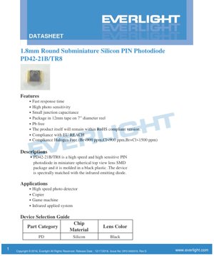
1. Product Overview
The PD42-21B/TR8 is a high-speed, high-sensitivity silicon PIN photodiode designed for infrared detection applications. Housed in a miniature 1.8mm diameter spherical top-view lens surface-mount device (SMD) package with a black plastic mold, this component is spectrally optimized to match common infrared emitting diodes. Its primary function is to convert incident light, particularly in the infrared spectrum, into an electrical current.
The device's core advantages stem from its fast response time, high photosensitivity, and small junction capacitance, making it suitable for applications requiring quick and reliable light detection. It is supplied in a tape-and-reel format compatible with automated assembly processes, adhering to modern environmental standards by being lead-free (Pb-free), RoHS compliant, EU REACH compliant, and halogen-free.
2. Technical Parameter Deep-Dive
2.1 Absolute Maximum Ratings
These ratings define the limits beyond which permanent damage to the device may occur. Operation under these conditions is not guaranteed.
- Reverse Voltage (VR): 32 V - The maximum voltage that can be applied in reverse bias across the photodiode terminals.
- Operating Temperature (Topr): -25°C to +85°C - The ambient temperature range for normal device operation.
- Storage Temperature (Tstg): -40°C to +85°C - The temperature range for non-operational storage.
- Soldering Temperature (Tsol): 260°C for a maximum of 5 seconds - The peak temperature limit during reflow soldering.
- Power Dissipation (Pd): 150 mW at 25°C - The maximum power the device can dissipate.
2.2 Electro-Optical Characteristics
These parameters, measured at 25°C, define the photodiode's performance under specified test conditions.
- Spectral Bandwidth (λ0.5): 730 nm to 1100 nm - The wavelength range where the photodiode's responsivity is at least half of its peak value. This defines its sensitivity window.
- Peak Sensitivity Wavelength (λP): 940 nm (Typical) - The wavelength of light at which the photodiode is most sensitive. This aligns it with common 940nm IR LEDs.
- Open-Circuit Voltage (VOC): 0.42 V (Typical) at Ee=5 mW/cm², λP=940nm - The voltage generated across the photodiode terminals under illumination when no current is drawn (open circuit).
- Short-Circuit Current (ISC): 4.0 μA (Typical) at Ee=1 mW/cm², λP=875nm - The current flowing through the photodiode when its terminals are short-circuited under illumination.
- Reverse Light Current (IL): 4.0 μA (Typical) at Ee=1 mW/cm², λP=875nm, VR=5V - The photocurrent generated when the device is reverse-biased. This is the primary operating parameter for most detection circuits.
- Dark Current (ID): 10 nA (Max) at VR=10V - The small reverse leakage current that flows when the device is in complete darkness. Lower values indicate better signal-to-noise ratio.
- Reverse Breakdown Voltage (VBR): 32 V (Min), 170 V (Typ) at IR=100μA - The voltage at which the reverse current increases sharply. Operating near or above this voltage can cause damage.
3. Performance Curve Analysis
The datasheet includes typical characteristic curves which provide visual insight into device behavior beyond single-point specifications.
3.1 Spectral Sensitivity (Fig. 1)
This curve plots the relative responsivity of the photodiode against the wavelength of incident light. It graphically confirms the spectral bandwidth and peak sensitivity at 940nm. The curve shows a sharp rise in sensitivity from around 700nm, peaking at 940nm, and then gradually falling off towards 1100nm. This shape is characteristic of silicon-based photodetectors.
3.2 Reverse Light Current vs. Irradiance (Fig. 2)
This graph illustrates the relationship between the generated photocurrent (IL) and the incident light power density (Ee). For a PIN photodiode operating in photoconductive mode (reverse-biased), this relationship is typically linear over a wide range. This linearity is crucial for analog light sensing applications where the output signal must be directly proportional to light intensity.
4. Mechanical and Package Information
4.1 Package Dimensions
The PD42-21B/TR8 is a round subminiature device with a 1.8mm body diameter. The detailed mechanical drawing provides all critical dimensions including overall height, lens shape, lead spacing, and pad recommendations. The suggested pad layout is for reference; designers should adjust based on their specific PCB design rules and thermal/mechanical requirements. All dimensional tolerances are typically ±0.1mm unless otherwise specified.
4.2 Polarity Identification
The device has two terminals. Correct polarity connection is essential for proper operation in a reverse-biased circuit. The datasheet drawing indicates the cathode and anode. Typically, the longer lead or a specific marking on the package denotes the cathode. Connecting the cathode to a more positive voltage (in reverse bias) is the standard operating condition.
4.3 Packaging Specification
The component is supplied in embossed carrier tape on 7-inch diameter reels. The tape dimensions (pocket size, pitch, etc.) are specified to ensure compatibility with standard SMD pick-and-place equipment. Each reel contains 1000 pieces, which is a common quantity for medium-volume production.
5. Soldering and Assembly Guidelines
5.1 Reflow Soldering Profile
The device is suitable for lead-free (Pb-free) reflow soldering processes. The maximum peak temperature must not exceed 260°C, and the time above 260°C should be limited. The total number of reflow cycles should not exceed two to prevent thermal stress damage to the plastic package and internal die attach.
5.2 Hand Soldering
If manual soldering is necessary, extreme care must be taken. The soldering iron tip temperature should be below 350°C, and contact time per lead should be limited to 3 seconds or less. A low-power iron (≤25W) is recommended. A cooling interval should be allowed between soldering each terminal to prevent localized overheating.
5.3 Rework and Repair
Rework after initial soldering is strongly discouraged. If unavoidable, a specialized double-head soldering iron should be used to simultaneously heat both terminals, allowing for safe removal without applying excessive mechanical stress. The potential impact on device performance from rework must be evaluated beforehand.
6. Storage and Handling Precautions
- Moisture Sensitivity: The device is moisture-sensitive. The bag should not be opened until ready for use. Pre-conditioning storage should be at ≤30°C and ≤90% RH.
- Floor Life: After opening the moisture barrier bag, components must be used within 168 hours (7 days) if stored at ≤30°C and ≤60% RH.
- Baking: If the storage time is exceeded or the desiccant indicates high humidity, a baking treatment at 60±5°C for 24 hours is required to remove absorbed moisture and prevent \"popcorning\" during reflow.
7. Application Suggestions
7.1 Typical Application Circuits
The primary application is as a high-speed photodetector. In a typical circuit, the photodiode is reverse-biased with a voltage below its maximum rating (e.g., 5V as in the test condition). The photocurrent (IL) flows through a load resistor (RL). The voltage drop across RL, which is proportional to the light intensity, is then amplified by a subsequent transimpedance amplifier (TIA) or voltage amplifier. The fast response time makes it suitable for pulsed light detection and data communication.
7.2 Design Considerations
- Bias Voltage: A reverse bias voltage (e.g., 5V) is recommended for optimal speed and linearity. Higher bias can reduce junction capacitance further, increasing bandwidth, but must stay below VR.
- Current Limiting/Protection: As noted in the precautions, the photodiode itself does not limit current. In circuits where it could be exposed to high-intensity light or connected incorrectly, a series resistor may be necessary to prevent excessive current that could damage the junction.
- Optical Design: The black lens helps reduce stray light sensitivity. For optimal performance, the photodiode should be paired with an IR source (like an 850nm or 940nm LED) and potentially an optical filter to block unwanted ambient light, especially visible light which it can also detect to some degree.
7.3 Application Scenarios
- High-Speed Photo Detection: Suitable for light barrier systems, object counting, and encoders where rapid on/off light transitions need to be detected.
- Copiers and Scanners: Can be used as a sensor to detect document presence, paper jam, or as part of the image sensing array in contact image sensors (CIS).
- Game Machines & Consumer Electronics: Used in IR remote control receivers, proximity sensors, and gesture recognition systems.
- Infrared Applied Systems: Any system utilizing modulated or pulsed infrared light for data transmission, distance measurement (time-of-flight), or simple presence detection.
8. Technical Comparison and Differentiation
Compared to standard PN photodiodes, the PIN structure offers key advantages: a wider depletion region (the \"I\" or intrinsic layer) which results in lower junction capacitance (enabling faster response) and allows it to operate efficiently at lower reverse bias voltages. The small 1.8mm package makes it ideal for space-constrained designs. The black lens provides a degree of built-in visible light suppression compared to clear-lens variants, which is beneficial in IR-specific applications.
9. Frequently Asked Questions (Based on Technical Parameters)
Q: What is the difference between short-circuit current (ISC) and reverse light current (IL)?
A: ISC is measured with zero voltage across the diode (photovoltaic mode). IL is measured with a reverse bias applied (photoconductive mode). IL is typically the parameter used in circuit design as it is more stable and linear, and the reverse bias speeds up the response.
Q: Why is the dark current important?
A: Dark current is the noise floor of the photodiode. In low-light applications, a high dark current can mask the small photocurrent signal, reducing sensitivity and signal-to-noise ratio. The max 10 nA spec is quite low for a silicon photodiode.
Q: Can I use this with a visible light source?
A: Yes, but with reduced efficiency. The spectral response curve shows it is sensitive from ~730nm, so it will detect red and near-infrared light well. For optimal performance with visible light (e.g., blue or green), a photodiode with a different spectral peak would be more appropriate.
10. Operational Principles
A PIN photodiode is a semiconductor device with a p-type region, an intrinsic (undoped) region, and an n-type region. When reverse-biased, a wide depletion region forms primarily across the intrinsic layer. Incident photons with energy greater than the semiconductor's bandgap are absorbed, creating electron-hole pairs. The strong electric field in the depletion region swiftly separates these pairs, causing them to drift to the respective terminals, thereby generating a photocurrent that is proportional to the incident light intensity. The intrinsic layer reduces capacitance and allows efficient carrier collection across a wider area, enhancing speed and quantum efficiency.
LED Specification Terminology
Complete explanation of LED technical terms
Photoelectric Performance
| Term | Unit/Representation | Simple Explanation | Why Important |
|---|---|---|---|
| Luminous Efficacy | lm/W (lumens per watt) | Light output per watt of electricity, higher means more energy efficient. | Directly determines energy efficiency grade and electricity cost. |
| Luminous Flux | lm (lumens) | Total light emitted by source, commonly called "brightness". | Determines if the light is bright enough. |
| Viewing Angle | ° (degrees), e.g., 120° | Angle where light intensity drops to half, determines beam width. | Affects illumination range and uniformity. |
| CCT (Color Temperature) | K (Kelvin), e.g., 2700K/6500K | Warmth/coolness of light, lower values yellowish/warm, higher whitish/cool. | Determines lighting atmosphere and suitable scenarios. |
| CRI / Ra | Unitless, 0–100 | Ability to render object colors accurately, Ra≥80 is good. | Affects color authenticity, used in high-demand places like malls, museums. |
| SDCM | MacAdam ellipse steps, e.g., "5-step" | Color consistency metric, smaller steps mean more consistent color. | Ensures uniform color across same batch of LEDs. |
| Dominant Wavelength | nm (nanometers), e.g., 620nm (red) | Wavelength corresponding to color of colored LEDs. | Determines hue of red, yellow, green monochrome LEDs. |
| Spectral Distribution | Wavelength vs intensity curve | Shows intensity distribution across wavelengths. | Affects color rendering and quality. |
Electrical Parameters
| Term | Symbol | Simple Explanation | Design Considerations |
|---|---|---|---|
| Forward Voltage | Vf | Minimum voltage to turn on LED, like "starting threshold". | Driver voltage must be ≥Vf, voltages add up for series LEDs. |
| Forward Current | If | Current value for normal LED operation. | Usually constant current drive, current determines brightness & lifespan. |
| Max Pulse Current | Ifp | Peak current tolerable for short periods, used for dimming or flashing. | Pulse width & duty cycle must be strictly controlled to avoid damage. |
| Reverse Voltage | Vr | Max reverse voltage LED can withstand, beyond may cause breakdown. | Circuit must prevent reverse connection or voltage spikes. |
| Thermal Resistance | Rth (°C/W) | Resistance to heat transfer from chip to solder, lower is better. | High thermal resistance requires stronger heat dissipation. |
| ESD Immunity | V (HBM), e.g., 1000V | Ability to withstand electrostatic discharge, higher means less vulnerable. | Anti-static measures needed in production, especially for sensitive LEDs. |
Thermal Management & Reliability
| Term | Key Metric | Simple Explanation | Impact |
|---|---|---|---|
| Junction Temperature | Tj (°C) | Actual operating temperature inside LED chip. | Every 10°C reduction may double lifespan; too high causes light decay, color shift. |
| Lumen Depreciation | L70 / L80 (hours) | Time for brightness to drop to 70% or 80% of initial. | Directly defines LED "service life". |
| Lumen Maintenance | % (e.g., 70%) | Percentage of brightness retained after time. | Indicates brightness retention over long-term use. |
| Color Shift | Δu′v′ or MacAdam ellipse | Degree of color change during use. | Affects color consistency in lighting scenes. |
| Thermal Aging | Material degradation | Deterioration due to long-term high temperature. | May cause brightness drop, color change, or open-circuit failure. |
Packaging & Materials
| Term | Common Types | Simple Explanation | Features & Applications |
|---|---|---|---|
| Package Type | EMC, PPA, Ceramic | Housing material protecting chip, providing optical/thermal interface. | EMC: good heat resistance, low cost; Ceramic: better heat dissipation, longer life. |
| Chip Structure | Front, Flip Chip | Chip electrode arrangement. | Flip chip: better heat dissipation, higher efficacy, for high-power. |
| Phosphor Coating | YAG, Silicate, Nitride | Covers blue chip, converts some to yellow/red, mixes to white. | Different phosphors affect efficacy, CCT, and CRI. |
| Lens/Optics | Flat, Microlens, TIR | Optical structure on surface controlling light distribution. | Determines viewing angle and light distribution curve. |
Quality Control & Binning
| Term | Binning Content | Simple Explanation | Purpose |
|---|---|---|---|
| Luminous Flux Bin | Code e.g., 2G, 2H | Grouped by brightness, each group has min/max lumen values. | Ensures uniform brightness in same batch. |
| Voltage Bin | Code e.g., 6W, 6X | Grouped by forward voltage range. | Facilitates driver matching, improves system efficiency. |
| Color Bin | 5-step MacAdam ellipse | Grouped by color coordinates, ensuring tight range. | Guarantees color consistency, avoids uneven color within fixture. |
| CCT Bin | 2700K, 3000K etc. | Grouped by CCT, each has corresponding coordinate range. | Meets different scene CCT requirements. |
Testing & Certification
| Term | Standard/Test | Simple Explanation | Significance |
|---|---|---|---|
| LM-80 | Lumen maintenance test | Long-term lighting at constant temperature, recording brightness decay. | Used to estimate LED life (with TM-21). |
| TM-21 | Life estimation standard | Estimates life under actual conditions based on LM-80 data. | Provides scientific life prediction. |
| IESNA | Illuminating Engineering Society | Covers optical, electrical, thermal test methods. | Industry-recognized test basis. |
| RoHS / REACH | Environmental certification | Ensures no harmful substances (lead, mercury). | Market access requirement internationally. |
| ENERGY STAR / DLC | Energy efficiency certification | Energy efficiency and performance certification for lighting. | Used in government procurement, subsidy programs, enhances competitiveness. |