1. Product Overview
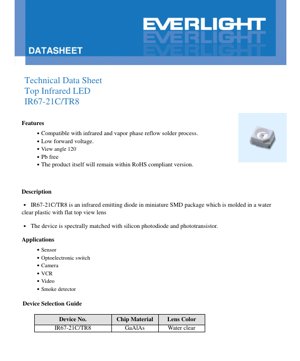
The IR67-21C/TR8 is a top-view infrared emitting diode housed in a miniature Surface-Mount Device (SMD) package. The device is molded in water-clear plastic with a flat top lens, designed for compatibility with modern infrared and vapor phase reflow soldering processes. Its primary function is to emit infrared light at a peak wavelength matched to silicon photodiodes and phototransistors, making it a core component in various sensing and switching applications.
The key advantages of this component include its low forward voltage requirement, a wide 120-degree viewing angle, and compliance with Pb-free and RoHS environmental standards. Its miniature SMD form factor allows for high-density placement on printed circuit boards, which is essential for compact consumer and industrial electronics.
1.1 Core Specifications and Device Selection
The fundamental specifications defining the IR67-21C/TR8 are its chip material and optical characteristics. The light-emitting chip is constructed from Gallium Aluminum Arsenide (GaAlAs), a semiconductor material well-suited for producing infrared radiation. The package features a water-clear lens, which does not filter the emitted infrared light, ensuring maximum radiant intensity output. This combination of GaAlAs chip and clear lens is specifically engineered for optimal performance in sensor applications where the detected signal strength is critical.
2. Technical Parameters: In-Depth Objective Interpretation
This section provides a detailed, objective analysis of the electrical, optical, and thermal parameters specified for the IR67-21C/TR8 infrared LED. Understanding these ratings is crucial for reliable circuit design and ensuring the long-term operational integrity of the device.
2.1 Absolute Maximum Ratings
The Absolute Maximum Ratings define the stress limits beyond which permanent damage to the device may occur. These are not recommended operating conditions but rather thresholds that must not be exceeded under any circumstance, including during transient events.
- Continuous Forward Current (IF): 65 mA. This is the maximum DC current that can be passed through the LED junction indefinitely at an ambient temperature (Ta) of 25°C.
- Peak Forward Current (IFP): 1.0 A. This high current is permissible only under strict pulsed conditions: pulse width ≤ 100 µs and duty cycle ≤ 1%. This rating is relevant for applications requiring brief, high-intensity pulses of IR light.
- Reverse Voltage (VR): 5 V. Applying a reverse bias voltage exceeding this value can cause junction breakdown.
- Power Dissipation (Pd): 130 mW at 25°C. This is the maximum power the package can dissipate as heat. The actual allowable power decreases as ambient temperature rises, as shown in the derating curve.
- Thermal Resistance, Junction-to-Ambient (Rthj-a): 400 K/W. This parameter quantifies how effectively heat travels from the semiconductor junction to the surrounding air. A lower value indicates better heat dissipation. With this value, for every watt of power dissipated, the junction temperature will rise 400°C above the ambient temperature.
- Soldering Temperature (Tsol): 260°C for a maximum of 5 seconds. This defines the reflow soldering profile tolerance.
2.2 Electro-Optical Characteristics
These parameters, measured at a standard test condition of 25°C, describe the device's performance under normal operation. The 'Typ.' column represents typical or expected values, while 'Min.' and 'Max.' define the guaranteed performance limits.
- Radiant Intensity (Ie): This is the optical power emitted per unit solid angle (measured in milliwatts per steradian, mW/sr). At a standard drive current of 20mA, the typical radiant intensity is 1.5 mW/sr, with a minimum of 1.0 mW/sr guaranteed. Under pulsed high-current conditions (100mA, ≤100µs, ≤1% duty), the intensity can reach a typical value of 20 mW/sr.
- Peak Wavelength (λp): 940 nm (typical). This is the wavelength at which the LED emits the most optical power. It is spectrally matched to the peak sensitivity of common silicon-based photodetectors.
- Spectral Bandwidth (Δλ): 45 nm (typical). This defines the range of wavelengths emitted, typically measured at half the maximum intensity (Full Width at Half Maximum, FWHM). A 45nm bandwidth centered at 940nm means significant emission occurs from approximately 917.5nm to 962.5nm.
- Forward Voltage (VF): At 20mA, the typical forward voltage is 1.2V, with a maximum of 1.5V. At the pulsed 100mA condition, VF increases to a typical 1.4V (max 1.8V). This low VF is beneficial for low-voltage and battery-powered applications.
- View Angle (2θ1/2): 120 degrees. This is the full angle where the radiant intensity drops to half of its peak value (measured on-axis). A wide 120° angle provides broad, diffuse illumination, ideal for proximity or presence sensing where the target position may vary.
3. Performance Curve Analysis
The datasheet includes several characteristic curves that illustrate how key parameters vary with operating conditions. These graphs are essential for dynamic system design.
3.1 Power Dissipation vs. Ambient Temperature
This derating curve shows that the maximum allowable power dissipation (Pd) decreases linearly from 130 mW at 25°C to 0 mW at approximately 150°C. Designers must use this graph to calculate the safe operating current for their specific maximum ambient temperature. For example, if the maximum ambient is 85°C, the graph indicates the permissible power dissipation is significantly reduced, which in turn limits the maximum allowable forward current.
3.2 Spectral Distribution
The spectral distribution curve plots relative radiant intensity against wavelength. It visually confirms the 940nm peak wavelength and the approximately 45nm spectral bandwidth. The curve is typically Gaussian in shape, centered on the peak wavelength.
3.3 Peak Emission Wavelength vs. Ambient Temperature
This curve demonstrates the temperature dependence of the peak wavelength. Typically, the peak wavelength of an LED shifts to longer wavelengths (a \"red shift\") as the junction temperature increases. The graph quantifies this shift, which is important for applications requiring precise spectral matching, as the detector's sensitivity may also be temperature-dependent.
3.4 Forward Current vs. Forward Voltage (I-V Curve)
The I-V curve is non-linear, like a standard diode. It shows the relationship between the current through the LED and the voltage across it. The \"knee\" of this curve is around the typical forward voltage. The curve helps in designing the current-limiting circuitry, especially for driving the LED with a voltage source.
3.5 Relative Radiant Intensity vs. Angular Displacement
This polar plot illustrates the spatial emission pattern. It confirms the 120° view angle, showing how intensity is distributed. The pattern for a flat-top LED in a clear package is typically close to a Lambertian distribution, where intensity is proportional to the cosine of the angle from the normal (center).
4. Mechanical and Packaging Information
4.1 Package Dimensions
The IR67-21C/TR8 is housed in a miniature SMD package. The dimensional drawing provides all critical measurements for PCB footprint design, including body length, width, height, lead spacing, and pad dimensions. Key dimensions include the overall size (e.g., approximately 3.2mm x 2.8mm, though exact values must be taken from the drawing), the distance between the solder pads, and the recommended land pattern for reliable soldering. All dimensions are in millimeters with a standard tolerance of ±0.1mm unless otherwise specified.
4.2 Polarity Identification
The package includes markings or features (such as a notch, beveled corner, or cathode mark) to identify the anode and cathode terminals. Correct polarity must be observed during assembly, as applying reverse bias can damage the device.
4.3 Carrier Tape and Reel Specifications
For automated assembly, the components are supplied on embossed carrier tape wound onto reels. The datasheet provides the carrier tape dimensions, including pocket size, pitch, and tape width. The reel typically contains 2000 pieces. These dimensions are critical for programming pick-and-place machines.
5. Soldering and Assembly Guidelines
Proper handling and soldering are critical to prevent damage to the LED and ensure long-term reliability.
5.1 Reflow Soldering Process
The device is compatible with infrared and vapor phase reflow processes. A recommended Pb-free solder temperature profile is provided, specifying preheat, soak, reflow peak temperature (not to exceed 260°C), and cooling rates. Reflow soldering should not be performed more than two times. Stress should not be applied to the LED body during heating, and the PCB should not be warped after soldering.
5.2 Hand Soldering
If hand soldering is necessary, extreme care is required. The soldering iron tip temperature must be below 350°C, and contact time per terminal should not exceed 3 seconds. A low-power iron (≤25W) is recommended. A cooling interval of at least 2 seconds should be observed between soldering each terminal. The datasheet strongly advises that hand soldering often leads to damage.
5.3 Rework and Repair
Repair after the LED has been soldered is not recommended. If unavoidable, a double-head soldering iron should be used to simultaneously heat both terminals, minimizing thermal stress. The potential for damaging the LED's characteristics during rework must be evaluated beforehand.
6. Storage and Moisture Sensitivity
The IR67-21C/TR8 is moisture-sensitive. Precautions must be taken to prevent popcorning (package cracking due to rapid vapor expansion) during reflow.
- The moisture-proof bag should not be opened until the components are ready for use.
- Before opening, store at ≤30°C and ≤90% Relative Humidity (RH). The shelf life is one year.
- After opening, store at ≤30°C and ≤70% RH. The \"floor life\" (time allowed out of the bag) is 168 hours (7 days).
- If the silica gel desiccant has changed color (indicating saturation) or the storage time is exceeded, a bake-out at 60 ±5°C for 24 hours is required before reflow.
7. Application Suggestions
7.1 Typical Application Scenarios
The IR67-21C/TR8 is designed for a wide range of optoelectronic applications where invisible infrared light is used for sensing or signaling.
- Sensors: Used as the light source in proximity sensors, object detection, and line-following robots.
- Optoelectronic Switches: Forms one half of an optical interrupter or slotted switch, where an object breaks the beam between the LED and a photodetector.
- Consumer Electronics: Remote control transmitters for TVs, VCRs, and other audio/video equipment (though often higher-power LEDs are used for longer range).
- Imaging: Infrared illumination for security cameras, especially in low-light or night-vision modes.
- Safety Devices: Can be used as a component in certain types of smoke detectors that use optical scattering principles.
7.2 Critical Design Considerations
- Current Limiting: An external current-limiting resistor is absolutely mandatory. The LED exhibits a sharp I-V characteristic, meaning a small increase in voltage causes a large increase in current, leading to immediate burnout if not properly controlled. The resistor value is calculated using Ohm's Law: R = (Vsupply - VF) / IF.
- Heat Management: While the SMD package dissipates heat through the PCB pads, careful attention must be paid to the power dissipation derating curve, especially in high-ambient-temperature environments. Adequate PCB copper area (thermal relief pads) can help lower the junction temperature.
- Spectral Matching: Ensure the selected photodetector (photodiode, phototransistor) has peak sensitivity around 940nm for optimal system signal-to-noise ratio.
- Optical Design: The 120° viewing angle provides broad coverage. For longer-range or more directed beams, secondary optics (lenses) may be required.
8. Packaging and Ordering Information
8.1 Packing Procedure
The LEDs are packed in moisture-proof aluminum bags containing desiccant and humidity indicator cards. The bags are labeled with critical information for traceability and correct application.
8.2 Label Specification
The label includes several fields: Customer's Part Number (CPN), Manufacturer's Part Number (P/N), Packing Quantity (QTY), Lot Number (LOT NO), and optical binning information such as Category (CAT, likely for radiant intensity) and Hue (HUE, for peak wavelength). A reference code (REF) may also be present.
9. Frequently Asked Questions (Based on Technical Parameters)
Q: What is the purpose of the 1.0A Peak Forward Current rating if the Continuous Current is only 65mA?
A: The peak current rating allows the LED to be driven with very short, high-power pulses. This is useful in applications like distance measurement (time-of-flight) or data transmission where a brief, intense burst of IR light is needed to overcome ambient noise or travel a longer distance, without generating excessive average heat.
Q: How do I determine the safe operating current for my application if the ambient temperature is 50°C?
A: You must use the Power Dissipation vs. Ambient Temperature derating curve. Find the point on the curve corresponding to 50°C to determine the maximum allowable power dissipation (Pd(max)) at that temperature. Then, using the typical forward voltage (VF) at your desired current, calculate the maximum safe current: IF(max) = Pd(max) / VF. Always include a safety margin.
Q: Can I use this LED for a TV remote control?
A> While it emits at the correct wavelength (940nm is standard for remotes), its radiant intensity at 20mA (1.5 mW/sr typical) may be lower than dedicated remote control LEDs, which are often driven harder or have different optics for longer range. It could work for short-range remotes, but for typical living room distances, a component specifically characterized for higher output might be more suitable.
Q: Why is the storage and baking procedure so specific?
A> The plastic SMD package can absorb moisture from the air. During the high-temperature reflow soldering process, this absorbed moisture can rapidly turn to steam, creating internal pressure that can delaminate the package or crack the die (\"popcorning\"). The controlled storage and baking procedures are industry-standard (based on JEDEC MSL ratings) to remove this moisture safely before soldering.
10. Operational Principles and Technology Context
10.1 Basic Operating Principle
An Infrared Light Emitting Diode (IR LED) operates on the principle of electroluminescence in a semiconductor p-n junction. When a forward voltage is applied, electrons from the n-type material and holes from the p-type material are injected into the junction region. When these charge carriers recombine, they release energy. In a GaAlAs semiconductor, this energy is released primarily as photons in the infrared spectrum (around 940nm). The specific wavelength is determined by the bandgap energy of the semiconductor material, which is engineered by adjusting the ratio of aluminum to gallium in the crystal.
10.2 Role in Optoelectronic Systems
In a typical sensing system, the IR67-21C/TR8 acts as the active signal source. Its light is either directly received by a detector (for transmission sensing), reflected off a target (for proximity/reflective sensing), or interrupted by an object (for break-beam sensing). The detector converts the modulated or interrupted IR light into an electrical signal for processing. The 940nm wavelength is ideal because it is invisible to the human eye, avoids interference from most ambient visible light, and aligns with the high sensitivity region of inexpensive silicon detectors while being less susceptible to absorption by air and common materials compared to longer IR wavelengths.
10.3 Industry Trends and Context
The development of SMD infrared LEDs like the IR67-21C/TR8 is driven by the miniaturization and automation of electronics assembly. The trend is towards smaller package footprints, higher radiant intensity per unit area, improved thermal performance, and tighter binning for consistent performance. There is also ongoing research into new semiconductor materials (like InGaN on silicon for different IR bands) and integrated solutions that combine the LED driver, sensor, and signal processing in a single module (e.g., proximity sensor modules). The demand for reliable, low-cost IR components continues to grow with the expansion of the Internet of Things (IoT), automotive sensing (e.g., in-cabin monitoring), and industrial automation.
LED Specification Terminology
Complete explanation of LED technical terms
Photoelectric Performance
| Term | Unit/Representation | Simple Explanation | Why Important |
|---|---|---|---|
| Luminous Efficacy | lm/W (lumens per watt) | Light output per watt of electricity, higher means more energy efficient. | Directly determines energy efficiency grade and electricity cost. |
| Luminous Flux | lm (lumens) | Total light emitted by source, commonly called "brightness". | Determines if the light is bright enough. |
| Viewing Angle | ° (degrees), e.g., 120° | Angle where light intensity drops to half, determines beam width. | Affects illumination range and uniformity. |
| CCT (Color Temperature) | K (Kelvin), e.g., 2700K/6500K | Warmth/coolness of light, lower values yellowish/warm, higher whitish/cool. | Determines lighting atmosphere and suitable scenarios. |
| CRI / Ra | Unitless, 0–100 | Ability to render object colors accurately, Ra≥80 is good. | Affects color authenticity, used in high-demand places like malls, museums. |
| SDCM | MacAdam ellipse steps, e.g., "5-step" | Color consistency metric, smaller steps mean more consistent color. | Ensures uniform color across same batch of LEDs. |
| Dominant Wavelength | nm (nanometers), e.g., 620nm (red) | Wavelength corresponding to color of colored LEDs. | Determines hue of red, yellow, green monochrome LEDs. |
| Spectral Distribution | Wavelength vs intensity curve | Shows intensity distribution across wavelengths. | Affects color rendering and quality. |
Electrical Parameters
| Term | Symbol | Simple Explanation | Design Considerations |
|---|---|---|---|
| Forward Voltage | Vf | Minimum voltage to turn on LED, like "starting threshold". | Driver voltage must be ≥Vf, voltages add up for series LEDs. |
| Forward Current | If | Current value for normal LED operation. | Usually constant current drive, current determines brightness & lifespan. |
| Max Pulse Current | Ifp | Peak current tolerable for short periods, used for dimming or flashing. | Pulse width & duty cycle must be strictly controlled to avoid damage. |
| Reverse Voltage | Vr | Max reverse voltage LED can withstand, beyond may cause breakdown. | Circuit must prevent reverse connection or voltage spikes. |
| Thermal Resistance | Rth (°C/W) | Resistance to heat transfer from chip to solder, lower is better. | High thermal resistance requires stronger heat dissipation. |
| ESD Immunity | V (HBM), e.g., 1000V | Ability to withstand electrostatic discharge, higher means less vulnerable. | Anti-static measures needed in production, especially for sensitive LEDs. |
Thermal Management & Reliability
| Term | Key Metric | Simple Explanation | Impact |
|---|---|---|---|
| Junction Temperature | Tj (°C) | Actual operating temperature inside LED chip. | Every 10°C reduction may double lifespan; too high causes light decay, color shift. |
| Lumen Depreciation | L70 / L80 (hours) | Time for brightness to drop to 70% or 80% of initial. | Directly defines LED "service life". |
| Lumen Maintenance | % (e.g., 70%) | Percentage of brightness retained after time. | Indicates brightness retention over long-term use. |
| Color Shift | Δu′v′ or MacAdam ellipse | Degree of color change during use. | Affects color consistency in lighting scenes. |
| Thermal Aging | Material degradation | Deterioration due to long-term high temperature. | May cause brightness drop, color change, or open-circuit failure. |
Packaging & Materials
| Term | Common Types | Simple Explanation | Features & Applications |
|---|---|---|---|
| Package Type | EMC, PPA, Ceramic | Housing material protecting chip, providing optical/thermal interface. | EMC: good heat resistance, low cost; Ceramic: better heat dissipation, longer life. |
| Chip Structure | Front, Flip Chip | Chip electrode arrangement. | Flip chip: better heat dissipation, higher efficacy, for high-power. |
| Phosphor Coating | YAG, Silicate, Nitride | Covers blue chip, converts some to yellow/red, mixes to white. | Different phosphors affect efficacy, CCT, and CRI. |
| Lens/Optics | Flat, Microlens, TIR | Optical structure on surface controlling light distribution. | Determines viewing angle and light distribution curve. |
Quality Control & Binning
| Term | Binning Content | Simple Explanation | Purpose |
|---|---|---|---|
| Luminous Flux Bin | Code e.g., 2G, 2H | Grouped by brightness, each group has min/max lumen values. | Ensures uniform brightness in same batch. |
| Voltage Bin | Code e.g., 6W, 6X | Grouped by forward voltage range. | Facilitates driver matching, improves system efficiency. |
| Color Bin | 5-step MacAdam ellipse | Grouped by color coordinates, ensuring tight range. | Guarantees color consistency, avoids uneven color within fixture. |
| CCT Bin | 2700K, 3000K etc. | Grouped by CCT, each has corresponding coordinate range. | Meets different scene CCT requirements. |
Testing & Certification
| Term | Standard/Test | Simple Explanation | Significance |
|---|---|---|---|
| LM-80 | Lumen maintenance test | Long-term lighting at constant temperature, recording brightness decay. | Used to estimate LED life (with TM-21). |
| TM-21 | Life estimation standard | Estimates life under actual conditions based on LM-80 data. | Provides scientific life prediction. |
| IESNA | Illuminating Engineering Society | Covers optical, electrical, thermal test methods. | Industry-recognized test basis. |
| RoHS / REACH | Environmental certification | Ensures no harmful substances (lead, mercury). | Market access requirement internationally. |
| ENERGY STAR / DLC | Energy efficiency certification | Energy efficiency and performance certification for lighting. | Used in government procurement, subsidy programs, enhances competitiveness. |