Table of Contents
- 1. Product Overview
- 2. Key Features and Core Advantages
- 3. Target Market and Applications
- 4. In-Depth Technical Parameter Analysis
- 4.1 Absolute Maximum Ratings
- 4.2 Electrical and Optoelectronic Characteristics
- 4.2.1 Input (Infrared LED) Characteristics
- 4.2.2 Output (Phototransistor) Characteristics
- 4.2.3 Transfer Characteristics
- 5. Mechanical and Package Information
- 5.1 Package Dimensions and Outline Drawings
- 5.2 Pin Configuration and Polarity
- 5.3 Recommended PCB Pad Layout
- 5.4 Device Marking
- 6. Soldering and Assembly Guidelines
- 7. Packaging and Ordering Information
- 7.1 Model Numbering System
- 7.2 Packaging Specifications
- 8. Application Design Considerations
- 8.1 Typical Application Circuits
- 8.2 Design Notes and Best Practices
- 9. Technical Comparison and Differentiation
- 10. Frequently Asked Questions (FAQs)
- 10.1 What is the maximum data rate achievable with these photocouplers?
- 10.2 How do I select the correct CTR bin for my application?
- 10.3 Can these devices be used to isolate analog signals?
- 10.4 What is the purpose of the isolation voltage rating, and how is it tested?
- 11. Practical Design Example
- 12. Operating Principle
- 13. Industry Trends and Development
1. Product Overview
The ELD3H7 and ELQ3H7 are phototransistor-based photocouplers (optocouplers) designed for electrical signal isolation. They consist of an infrared light-emitting diode (LED) optically coupled to a silicon phototransistor, all encapsulated within a compact surface-mount package. The primary function is to transmit electrical signals between two circuits while maintaining high electrical isolation, preventing noise, ground loops, and voltage spikes from propagating.
The ELD3H7 integrates 2 independent isolation channels within an 8-pin SSOP (Shrink Small Outline Package). The ELQ3H7 integrates 4 independent channels within a 16-pin SSOP. Both variants feature an ultra-low profile of 2.0 mm, making them suitable for space-constrained applications. The devices use a halogen-free, green molding compound and are compliant with Pb-free and RoHS directives.
2. Key Features and Core Advantages
- High Isolation Voltage: Rated at 3750 Vrms for 1 minute, ensuring robust protection and safety in high-voltage environments.
- Wide Current Transfer Ratio (CTR): Ranges from 50% to 600% at IF = 5mA, VCE = 5V, offering design flexibility for different signal amplification needs.
- Compact Form Factor: The SSOP package with a 2.0 mm profile is ideal for high-density PCB designs.
- Comprehensive Safety Approvals: Certified by UL (E214129), VDE (40028116), SEMKO, NEMKO, DEMKO, FIMKO, and CQC, facilitating use in globally regulated equipment.
- Fast Switching Characteristics: Typical rise time (tr) of 5 µs and fall time (tf) of 3 µs under specified test conditions, suitable for digital signal transmission.
3. Target Market and Applications
These photocouplers are engineered for applications requiring reliable signal isolation and noise immunity.
- DC-DC Converters: Providing feedback loop isolation in switch-mode power supplies.
- Programmable Logic Controllers (PLCs) & Industrial Automation: Isolating digital I/O signals between the controller and field devices.
- Telecommunication Equipment: Isolating signal lines in modems, interfaces, and network hardware.
- General Circuit Isolation: Transmitting signals between circuits of different ground potentials or impedance levels.
4. In-Depth Technical Parameter Analysis
4.1 Absolute Maximum Ratings
These are stress limits that must not be exceeded under any conditions to prevent permanent device damage.
- Input (LED Side): Forward current (IF) 60 mA; Peak forward current (IFP) 1 A for 1 µs pulse; Reverse voltage (VR) 6 V; Power dissipation (PD) 70 mW.
- Output (Transistor Side): Collector current (IC) 50 mA; Collector-Emitter voltage (VCEO) 80 V; Emitter-Collector voltage (VECO) 7 V; Power dissipation (PC) 150 mW.
- Total Device: Total power dissipation (PTOT) 200 mW; Isolation voltage (VISO) 3750 Vrms.
- Temperature: Operating range -55°C to +110°C; Storage range -55°C to +125°C; Soldering temperature 260°C for 10 seconds.
4.2 Electrical and Optoelectronic Characteristics
Typical performance parameters measured at 25°C.
4.2.1 Input (Infrared LED) Characteristics
- Forward Voltage (VF): Typically 1.2V, maximum 1.4V at IF=20mA. This parameter is crucial for designing the LED drive circuit.
- Reverse Current (IR): Maximum 10 µA at VR=4V, indicating good diode blocking characteristics.
- Input Capacitance (Cin): Typically 30 pF, affecting high-frequency switching performance.
4.2.2 Output (Phototransistor) Characteristics
- Dark Current (ICEO): Maximum 100 nA at VCE=20V with IF=0mA. This is the leakage current when the LED is off, impacting the OFF-state signal integrity.
- Breakdown Voltages: BVCEO ≥ 80V, BVECO ≥ 7V, defining the maximum allowable voltages across the transistor.
- Collector-Emitter Saturation Voltage (VCE(sat)): Typically 0.1V, maximum 0.2V at IF=10mA, IC=1mA. A low VCE(sat) is desirable for logic-level output.
4.2.3 Transfer Characteristics
- Current Transfer Ratio (CTR): Defined as (IC / IF) * 100%. The specified range is 50% to 600% at IF=5mA, VCE=5V. This wide binning allows selection based on required gain.
- Isolation Resistance (RIO): Minimum 5×10¹⁰ Ω at 500V DC, ensuring excellent DC isolation.
- Isolation Capacitance (CIO): Typically 0.3 pF, maximum 1.0 pF. A low capacitance minimizes capacitive coupling of high-frequency noise across the isolation barrier.
- Switching Times: Rise time (tr) typically 5 µs, fall time (tf) typically 3 µs under test conditions (VCE=2V, IC=2mA, RL=100Ω). These values determine the maximum usable data rate.
5. Mechanical and Package Information
5.1 Package Dimensions and Outline Drawings
The devices are housed in SSOP packages. The ELD3H7 (2-channel) uses an 8-pin SSOP, while the ELQ3H7 (4-channel) uses a 16-pin SSOP. Both share a common low profile height of 2.0 mm. Detailed dimensional drawings with all critical measurements (body size, lead pitch, standoff) are provided in the datasheet for PCB footprint design.
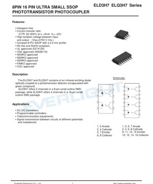
5.2 Pin Configuration and Polarity
For ELD3H7 (8-pin):
- Pins 1, 3: Anode of Channel 1 and Channel 2 LEDs, respectively.
- Pins 2, 4: Cathode of Channel 1 and Channel 2 LEDs, respectively.
- Pins 5, 7: Emitter of Channel 1 and Channel 2 phototransistors, respectively.
- Pins 6, 8: Collector of Channel 1 and Channel 2 phototransistors, respectively.
- Pins 1, 3, 5, 7: Anode of Channels 1 to 4 LEDs.
- Pins 2, 4, 6, 8: Cathode of Channels 1 to 4 LEDs.
- Pins 9, 11, 13, 15: Emitter of Channels 1 to 4 phototransistors.
- Pins 10, 12, 14, 16: Collector of Channels 1 to 4 phototransistors.
5.3 Recommended PCB Pad Layout
The datasheet includes suggested land pattern designs for both the 8-pin and 16-pin SSOP packages. Adhering to these recommendations ensures reliable solder joint formation during reflow soldering and proper mechanical stability.
5.4 Device Marking
Devices are marked on the top surface. The marking includes:
- "EL": Manufacturer identifier.
- "D3H7" or "Q3H7": Device number for the 2-channel or 4-channel variant.
- "Y": A one-digit year code.
- "WW": A two-digit week code.
- "V": Optional marking indicating VDE approval.
6. Soldering and Assembly Guidelines
The devices are suitable for surface-mount assembly using reflow soldering techniques.
- Reflow Soldering: The maximum allowable soldering temperature is 260°C, measured at the package body, for a duration not exceeding 10 seconds. Standard lead-free reflow profiles (IPC/JEDEC J-STD-020) are applicable.
- Handling: Standard ESD (Electrostatic Discharge) precautions should be observed, as the device contains static-sensitive semiconductors.
- Cleaning: Follow standard PCB cleaning procedures compatible with the green epoxy molding compound.
- Storage: Store in a dry environment with temperature between -55°C and +125°C. Use within 12 months of the date code for optimal solderability.
7. Packaging and Ordering Information
7.1 Model Numbering System
The part number follows the format: EL[D3H7/Q3H7](Z)-V
- EL: Series prefix.
- D3H7 / Q3H7: Denotes the 2-channel or 4-channel device.
- (Z): Tape and reel packaging option. "TA" indicates tape and reel, while its absence indicates tube packaging.
- V: Optional suffix indicating VDE approval.
7.2 Packaging Specifications
- ELD3H7 (Tube): 80 units per tube.
- ELD3H7 (Tape & Reel): 1000 units per reel.
- ELQ3H7 (Tube): 40 units per tube.
- ELQ3H7 (Tape & Reel): 1000 units per reel.
The tape and reel specifications, including carrier tape width, pocket dimensions, and reel diameter, are detailed for automated pick-and-place machine setup.
8. Application Design Considerations
8.1 Typical Application Circuits
The most common application is digital signal isolation. A series current-limiting resistor must be connected to the LED anode to set the desired forward current (IF). The value is calculated as Rlimit = (VCC_input - VF) / IF. On the output side, a pull-up resistor (RL) is connected between the collector and the output side supply voltage (VCC_output) to define the output logic levels and limit the phototransistor collector current.
8.2 Design Notes and Best Practices
- CTR Selection: Choose a CTR bin appropriate for your drive current and required output current. A higher CTR allows using a lower IF for the same output, reducing input power.
- Speed vs. Current Trade-off: Switching speed (tr, tf) generally improves with higher IF and lower RL, but this increases power consumption. The test circuit (IF pulse, VCE=2V, IC=2mA, RL=100Ω) provides a reference for expected performance.
- Noise Immunity: The high isolation resistance (RIO) and low isolation capacitance (CIO) are key for rejecting common-mode noise. Ensure proper PCB layout to avoid creepage and clearance issues that could compromise the rated isolation voltage.
- Thermal Considerations: Do not exceed the total device power dissipation (PTOT = 200 mW). Power is the sum of input LED power (IF*VF) and output transistor power (IC*VCE).
9. Technical Comparison and Differentiation
Compared to standard DIP-4 or DIP-6 photocouplers, the ELD3H7/ELQ3H7 series offers significant advantages:
- Size Reduction: The SSOP package occupies less than 25% of the board area of a standard DIP-8 package for a 2-channel device, enabling miniaturization.
- Multi-Channel Integration: The availability of 2 and 4 channels in single packages reduces component count and saves board space in multi-isolation applications.
- Profile: The 2.0 mm height is critical for ultra-thin designs.
- Performance: Maintains high isolation voltage and a wide CTR range despite the small size, a key differentiator from many miniaturized alternatives.
10. Frequently Asked Questions (FAQs)
10.1 What is the maximum data rate achievable with these photocouplers?
Based on the typical rise/fall times of 5 µs and 3 µs, the maximum practical data rate for a clean digital signal is approximately 1/(tr+tf) ≈ 125 kHz. For reliable operation, a conservative design target of 50-100 kHz is recommended.
10.2 How do I select the correct CTR bin for my application?
If your design requires a guaranteed minimum output current (IC) with a specific input current (IF), calculate the required minimum CTR: CTRmin_req = (IC / IF) * 100%. Select a device whose minimum guaranteed CTR (e.g., 50%) meets or exceeds this value. Using a higher CTR bin provides more design margin.
10.3 Can these devices be used to isolate analog signals?
While primarily designed for digital isolation, they can be used in low-frequency, low-precision analog applications (e.g., feedback in isolated power supplies). However, the CTR has a strong temperature dependence and nonlinearity with IF, which makes them unsuitable for precision analog signal transmission without extensive calibration or compensation circuits. Specialized linear optocouplers are better suited for analog isolation.
10.4 What is the purpose of the isolation voltage rating, and how is it tested?
The 3750 Vrms rating (for 1 minute) is a safety specification indicating the dielectric strength of the insulation between the input and output sides. During testing, all pins on the LED side are shorted together, and all pins on the transistor side are shorted together. A high AC voltage is applied between these two groups. This rating ensures protection against high-voltage transients that may occur in industrial or mains-connected equipment.
11. Practical Design Example
Scenario: Isolating a 3.3V digital signal from a microcontroller to a 5V system.
- Input Side: VCC_input = 3.3V. Target IF = 5 mA for good speed and CTR. Assuming VF ≈ 1.2V, Rlimit = (3.3V - 1.2V) / 0.005A = 420Ω. Use a standard 430Ω resistor.
- Output Side: VCC_output = 5V. Choose RL to limit IC and set logic levels. For a CTR of 100% at IF=5mA, IC ≈ 5mA. When the transistor is ON (saturated), VCE ≈ 0.1V, so the output is low (~0.1V). When OFF, the output is pulled high to 5V. The power in RL when ON is (5V - 0.1V) * 5mA ≈ 24.5 mW, well within ratings. A standard 1 kΩ resistor would give IC ≈ (5V - 0.1V)/1kΩ = 4.9mA, which is also acceptable.
- Layout: Place the device close to the isolation barrier on the PCB. Maintain recommended creepage and clearance distances (consult safety standards like IEC 60950-1) between the input and output copper traces, especially for the high isolation voltage rating.
12. Operating Principle
A photocoupler operates by converting an electrical signal into light, transmitting it across an electrically insulating gap, and then converting the light back into an electrical signal. In the ELD3H7/ELQ3H7:
- An electrical current (IF) flows through the infrared LED, causing it to emit photons.
- These photons travel through a transparent insulating dielectric (the molding compound) and strike the base region of the silicon phototransistor.
- The photon energy generates electron-hole pairs in the base, effectively creating a base current that turns the transistor ON.
- The transistor conducts a collector current (IC) that is proportional to the intensity of the received light, and hence to the input IF. The proportionality constant is the CTR.
13. Industry Trends and Development
The trend in optocoupler technology is driven by demands for higher speed, smaller size, lower power consumption, and integration of additional features. While traditional phototransistor couplers like the ELD3H7/ELQ3H7 excel in cost-effectiveness, robustness, and high isolation voltage, newer technologies are emerging:
- High-Speed Digital Couplers: Utilize CMOS technology and integrated LEDs to achieve data rates in the tens or hundreds of Mbps, far exceeding phototransistor-based devices.
- Integrated Isolated Functions: Devices that combine isolation with functions like isolated gate drivers, isolated ADCs, or isolated power delivery (isoPower).
- Enhanced Safety and Reliability: Ongoing development focuses on improving isolation material durability, surge immunity, and achieving higher working voltage ratings in smaller packages to meet evolving international safety standards.
LED Specification Terminology
Complete explanation of LED technical terms
Photoelectric Performance
| Term | Unit/Representation | Simple Explanation | Why Important |
|---|---|---|---|
| Luminous Efficacy | lm/W (lumens per watt) | Light output per watt of electricity, higher means more energy efficient. | Directly determines energy efficiency grade and electricity cost. |
| Luminous Flux | lm (lumens) | Total light emitted by source, commonly called "brightness". | Determines if the light is bright enough. |
| Viewing Angle | ° (degrees), e.g., 120° | Angle where light intensity drops to half, determines beam width. | Affects illumination range and uniformity. |
| CCT (Color Temperature) | K (Kelvin), e.g., 2700K/6500K | Warmth/coolness of light, lower values yellowish/warm, higher whitish/cool. | Determines lighting atmosphere and suitable scenarios. |
| CRI / Ra | Unitless, 0–100 | Ability to render object colors accurately, Ra≥80 is good. | Affects color authenticity, used in high-demand places like malls, museums. |
| SDCM | MacAdam ellipse steps, e.g., "5-step" | Color consistency metric, smaller steps mean more consistent color. | Ensures uniform color across same batch of LEDs. |
| Dominant Wavelength | nm (nanometers), e.g., 620nm (red) | Wavelength corresponding to color of colored LEDs. | Determines hue of red, yellow, green monochrome LEDs. |
| Spectral Distribution | Wavelength vs intensity curve | Shows intensity distribution across wavelengths. | Affects color rendering and quality. |
Electrical Parameters
| Term | Symbol | Simple Explanation | Design Considerations |
|---|---|---|---|
| Forward Voltage | Vf | Minimum voltage to turn on LED, like "starting threshold". | Driver voltage must be ≥Vf, voltages add up for series LEDs. |
| Forward Current | If | Current value for normal LED operation. | Usually constant current drive, current determines brightness & lifespan. |
| Max Pulse Current | Ifp | Peak current tolerable for short periods, used for dimming or flashing. | Pulse width & duty cycle must be strictly controlled to avoid damage. |
| Reverse Voltage | Vr | Max reverse voltage LED can withstand, beyond may cause breakdown. | Circuit must prevent reverse connection or voltage spikes. |
| Thermal Resistance | Rth (°C/W) | Resistance to heat transfer from chip to solder, lower is better. | High thermal resistance requires stronger heat dissipation. |
| ESD Immunity | V (HBM), e.g., 1000V | Ability to withstand electrostatic discharge, higher means less vulnerable. | Anti-static measures needed in production, especially for sensitive LEDs. |
Thermal Management & Reliability
| Term | Key Metric | Simple Explanation | Impact |
|---|---|---|---|
| Junction Temperature | Tj (°C) | Actual operating temperature inside LED chip. | Every 10°C reduction may double lifespan; too high causes light decay, color shift. |
| Lumen Depreciation | L70 / L80 (hours) | Time for brightness to drop to 70% or 80% of initial. | Directly defines LED "service life". |
| Lumen Maintenance | % (e.g., 70%) | Percentage of brightness retained after time. | Indicates brightness retention over long-term use. |
| Color Shift | Δu′v′ or MacAdam ellipse | Degree of color change during use. | Affects color consistency in lighting scenes. |
| Thermal Aging | Material degradation | Deterioration due to long-term high temperature. | May cause brightness drop, color change, or open-circuit failure. |
Packaging & Materials
| Term | Common Types | Simple Explanation | Features & Applications |
|---|---|---|---|
| Package Type | EMC, PPA, Ceramic | Housing material protecting chip, providing optical/thermal interface. | EMC: good heat resistance, low cost; Ceramic: better heat dissipation, longer life. |
| Chip Structure | Front, Flip Chip | Chip electrode arrangement. | Flip chip: better heat dissipation, higher efficacy, for high-power. |
| Phosphor Coating | YAG, Silicate, Nitride | Covers blue chip, converts some to yellow/red, mixes to white. | Different phosphors affect efficacy, CCT, and CRI. |
| Lens/Optics | Flat, Microlens, TIR | Optical structure on surface controlling light distribution. | Determines viewing angle and light distribution curve. |
Quality Control & Binning
| Term | Binning Content | Simple Explanation | Purpose |
|---|---|---|---|
| Luminous Flux Bin | Code e.g., 2G, 2H | Grouped by brightness, each group has min/max lumen values. | Ensures uniform brightness in same batch. |
| Voltage Bin | Code e.g., 6W, 6X | Grouped by forward voltage range. | Facilitates driver matching, improves system efficiency. |
| Color Bin | 5-step MacAdam ellipse | Grouped by color coordinates, ensuring tight range. | Guarantees color consistency, avoids uneven color within fixture. |
| CCT Bin | 2700K, 3000K etc. | Grouped by CCT, each has corresponding coordinate range. | Meets different scene CCT requirements. |
Testing & Certification
| Term | Standard/Test | Simple Explanation | Significance |
|---|---|---|---|
| LM-80 | Lumen maintenance test | Long-term lighting at constant temperature, recording brightness decay. | Used to estimate LED life (with TM-21). |
| TM-21 | Life estimation standard | Estimates life under actual conditions based on LM-80 data. | Provides scientific life prediction. |
| IESNA | Illuminating Engineering Society | Covers optical, electrical, thermal test methods. | Industry-recognized test basis. |
| RoHS / REACH | Environmental certification | Ensures no harmful substances (lead, mercury). | Market access requirement internationally. |
| ENERGY STAR / DLC | Energy efficiency certification | Energy efficiency and performance certification for lighting. | Used in government procurement, subsidy programs, enhances competitiveness. |