1. Product Overview
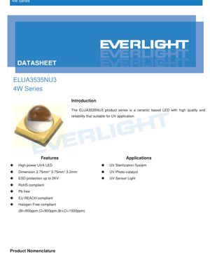
The ELUA3535NU3 product series represents a high-reliability, ceramic-based LED solution engineered specifically for ultraviolet-A (UVA) applications. This 4W series is designed to deliver consistent performance in demanding environments where UV radiation is utilized for its germicidal or catalytic properties.
1.1 Core Advantages and Target Market
The primary advantages of this LED series stem from its robust construction and electrical design. The use of an Aluminum Nitride (AlN) ceramic substrate provides excellent thermal conductivity, which is critical for managing the heat generated by high-power operation and ensuring long-term reliability. The device incorporates built-in Electrostatic Discharge (ESD) protection rated up to 2KV (HBM), enhancing its durability during handling and assembly. Furthermore, the product is fully compliant with major environmental and safety regulations including RoHS, Pb-free, EU REACH, and halogen-free standards (Br<900ppm, Cl<900ppm, Br+Cl<1500ppm), making it suitable for global markets with strict compliance requirements.
The target applications are primarily in the industrial and commercial sectors that leverage UVA light. Key markets include UV sterilization systems for air and water purification, UV photocatalyst systems for breaking down volatile organic compounds (VOCs), and specialized UV sensor lighting. The product's reliability and power output make it a suitable component for systems requiring sustained UV emission.
2. Technical Parameter Deep-Dive
This section provides a detailed, objective interpretation of the key technical parameters listed in the datasheet, explaining their significance for design engineers.
2.1 Absolute Maximum Ratings
The Absolute Maximum Ratings define the stress limits beyond which permanent damage to the device may occur. For the 385nm, 395nm, and 405nm variants, the maximum continuous forward current (IF) is 1250mA. It is crucial to note that the 365nm variant has a significantly lower maximum current rating of 700mA. This difference is typically due to the different semiconductor materials and epitaxial structures used for shorter wavelengths, which may have lower current handling capabilities or higher thermal sensitivity. Operating consistently at or near these limits will drastically reduce the LED's lifespan and reliability. The maximum junction temperature (TJ) is rated at 105°C. The thermal resistance from junction to thermal pad (Rθth) is specified as 4°C/W. This parameter is vital for thermal management design; for example, at the full rated current, the temperature rise from the pad to the junction can be calculated. Proper heatsinking is essential to keep the junction temperature within safe limits.
2.2 Photometric and Electrical Characteristics
The provided order codes detail specific performance bins. Radiant flux, the measure of total optical power output in watts (or milliwatts), varies by wavelength. For the 365nm LED (operating at 700mA), the minimum radiant flux is 900mW, typical is 1300mW, and maximum is 1600mW. For the 385nm, 395nm, and 405nm LEDs (operating at 1000mA), the minimum is 1350mW, typical is 1475mW, and maximum is 1850mW. The forward voltage (VF) for all models in the series is specified within a range of 3.6V to 4.8V at their respective operating currents. This range must be considered when designing the driver circuit to ensure it can provide sufficient voltage while managing power dissipation.
3. Binning System Explanation
The product is classified into bins based on three key parameters: Radiant Flux, Peak Wavelength, and Forward Voltage. This allows customers to select LEDs with tightly grouped characteristics for consistent system performance.
3.1 Radiant Flux Binning
Two separate binning tables are used for different wavelength groups. For the 365nm LED, bin codes U1 through U4 categorize radiant flux from 900-1000mW up to 1400-1600mW. For the 385nm to 405nm LEDs, bin codes U51 (1350-1600mW) and U52 (1600-1850mW) are used. Designers must ensure their optical system's minimum required irradiance is met by the minimum value of the selected bin.
3.2 Peak Wavelength Binning
Peak wavelength is binned into 10nm ranges: U36 (360-370nm), U38 (380-390nm), U39 (390-400nm), and U40 (400-410nm). The selection depends on the application's spectral sensitivity. For example, photocatalyst activation often has an optimal wavelength range.
3.3 Forward Voltage Binning
Forward voltage is binned into three groups: 3640 (3.6-4.0V), 4044 (4.0-4.4V), and 4448 (4.4-4.8V). This is important for driver efficiency and thermal management. LEDs from a lower voltage bin will dissipate less power as heat (P = VF * IF) at the same current, potentially allowing for a simpler or smaller heatsink.
4. Performance Curve Analysis
The typical characteristic curves provide insight into the LED's behavior under various operating conditions, which is essential for robust system design.
4.1 Spectrum and Relative Radiant Flux vs. Current
The spectrum graph shows the normalized emission intensity across wavelengths for the four main variants. Each has a distinct peak, with relatively narrow spectral bandwidths typical of UV LEDs. The Relative Radiant Flux vs. Forward Current curve shows a sub-linear relationship. The output does not increase proportionally with current, especially at higher currents, due to efficiency droop caused by increased junction temperature and other semiconductor physics effects. This highlights the importance of thermal management to maintain output.
4.2 Thermal Characteristics
The curves for Relative Radiant Flux vs. Ambient Temperature and Peak Wavelength vs. Ambient Temperature are critical. As ambient (or pad) temperature increases, the radiant flux decreases significantly—a common trait in LEDs. For instance, at 120°C, the relative flux is only about 40-50% of its value at 25°C. Concurrently, the peak wavelength shifts to longer wavelengths (red-shift) with increasing temperature, at a rate observable on the graph. This thermal shift must be accounted for in wavelength-sensitive applications. The Forward Voltage vs. Temperature curve shows a negative temperature coefficient, meaning VF decreases as temperature rises, which can affect constant-current driver operation.
5. Mechanical and Packaging Information
5.1 Dimensions and Tolerances
The LED features a compact footprint of 3.75mm x 3.75mm with an overall height of 3.2mm. The dimensional drawing specifies all critical lengths, including the thermal pad and anode/cathode pads. General tolerance on planar dimensions is ±0.1mm, while the thickness tolerance is ±0.15mm. These tolerances are important for PCB layout, solder paste stencil design, and ensuring proper placement by pick-and-place machines.
5.2 Pad Configuration and Polarity
The bottom view clearly shows the pad layout. The central, large rectangular pad is the thermal pad (cathode), which is essential for heat transfer to the PCB. Two smaller electrical pads are located on one side: one for the anode and one for the cathode. The polarity is indicated in the diagram. The cathode is typically connected to the thermal pad and one of the smaller pads. Correct polarity identification during assembly is mandatory to prevent device failure.
6. Soldering and Assembly Guidelines
6.1 Reflow Soldering Process
The LED is suitable for standard Surface-Mount Technology (SMT) processes. The datasheet provides a reflow profile graph with key parameters: a preheat zone, a rapid temperature rise to the peak, and a controlled cooling phase. The recommended peak temperature is 260°C (+0°C/-5°C) for 10 seconds maximum. It is explicitly stated that reflow soldering should not be performed more than twice to avoid undue thermal stress on the package and internal bonds. Mechanical stress on the LED body during heating (e.g., from PCB warpage) must be avoided, and bending the PCB after soldering is prohibited as it can crack the solder joints or the ceramic package itself.
7. Packaging and Ordering Information
7.1 Model Nomenclature Decoding
The full order code (e.g., ELUA3535NU3-P6070U23648700-V41G) is a detailed descriptor:
- EL: Manufacturer prefix.
- UA: UVA product type.
- 3535: 3.75mm x 3.75mm package size.
- N: Package material is Aluminum Nitride (AlN).
- U: Coating is Gold (Au).
- 3: Viewing angle is 30°.
- PXXXX: Peak wavelength code (e.g., 6070 for 360-370nm).
- YY: Minimum Radiant Flux code.
- 3648 / 700 / 1K0: Forward Voltage range (3.6-4.8V) and Forward Current (700mA or 1000mA).
- V41G: Chip type (Vertical), size (43mil), quantity (1), and process (Quartz Glass).
8. Application Recommendations
8.1 Typical Application Scenarios
UV Sterilization Systems: For air or water disinfection, the 265-280nm range (UVC) is most effective for DNA damage. However, UVA LEDs (like this series) are used in some advanced oxidation processes (AOP) or in systems targeting specific pathogens sensitive to longer UV, or in combination with photocatalysts. System design must ensure sufficient UV dose (intensity x time).
UV Photocatalyst: Typically using TiO2, photocatalysts are activated by UV light. The 385nm or 395nm variants are commonly used. The design must ensure uniform illumination of the catalyst surface and manage heat, as catalyst efficiency can be temperature-dependent.
UV Sensor Light: Used to excite fluorescence or for machine vision inspection. The stable output and specific wavelength are key. A constant current driver is essential to maintain stable optical output, and optical filters may be needed to block unwanted visible light from the LED's spectrum.
8.2 Critical Design Considerations
Thermal Management: This is the single most critical factor for performance and longevity. Use a PCB with adequate thermal vias under the thermal pad, connected to large copper planes or an external heatsink. The 4°C/W thermal resistance is from junction to the LED's thermal pad; the system thermal resistance to ambient must be designed to keep TJ well below 105°C.
Electrical Drive: Always use a constant current driver, not a constant voltage source. The driver must be capable of supplying the required current (700mA or 1000mA) and a voltage that covers the entire VF range of the selected bin, plus some headroom. Consider implementing pulse-width modulation (PWM) for dimming if needed, rather than analog current reduction, to avoid color/wavelength shift.
Optical Design: The 30° viewing angle provides a relatively focused beam. Lenses or reflectors may be used to shape the light for the target area. Ensure any optical materials (lenses, windows) are UV-transparent (e.g., quartz, specific UV-grade plastics) as standard glass and many plastics absorb UVA radiation.
9. Technical Comparison and Differentiation
While a direct side-by-side comparison with other brands is not provided in the datasheet, key differentiating features of this series can be inferred. The use of a ceramic AlN package offers superior thermal performance compared to plastic packages commonly used in lower-power LEDs, enabling higher drive currents and better reliability. The inclusion of 2KV ESD protection is a significant robustness feature not always present in competing products. The detailed binning across three parameters (flux, wavelength, voltage) allows for high-precision system design and consistency in mass production, which may be an advantage over products with looser tolerances or fewer binning options.
10. Frequently Asked Questions (Based on Technical Parameters)
Q: Why is the maximum current for the 365nm LED only 700mA, while the others are 1250mA?
A: This is primarily due to the different semiconductor material properties used to achieve the shorter 365nm wavelength. The material system (e.g., higher aluminum content in AlGaN) typically has lower electrical conductivity and higher defect densities, leading to reduced maximum current density and higher thermal resistance. Operating at a lower current ensures reliability and prevents accelerated degradation.
Q: Can I drive this LED with a 3.3V power supply?
A: No. The forward voltage range is 3.6V to 4.8V. A 3.3V supply will not be sufficient to turn on the LED or achieve any meaningful light output. A driver circuit that can provide at least 4.8V (plus driver dropout voltage) is required.
Q: How do I interpret the \"Typical Radiant Flux\" value?
A: The \"Typical\" value is a statistical average or median of production units. For guaranteed performance in your design, you must use the \"Minimum\" value from the binning table. Designing to the typical value may result in some units in your system underperforming.
Q: Is a heatsink absolutely necessary?
A> For any sustained operation at the rated current, yes. Even with the low 4°C/W thermal resistance, at 1000mA and a typical VF of 4.2V, the power dissipation is 4.2W. The temperature rise from pad to junction would be approximately 4.2W * 4°C/W = 16.8°C. If the PCB pad temperature reaches 85°C, the junction is already at ~102°C, very close to the 105°C maximum. Effective heatsinking is non-negotiable for reliable operation.
11. Practical Design and Usage Case
Case: Designing a PCB for a Multi-LED UV Array for Surface Curing.
An engineer is designing an array of twelve 395nm LEDs for a low-power UV curing station for adhesives. Each LED will be driven at 1000mA. Step 1 - PCB Layout: The PCB is designed with 2oz copper. A dedicated thermal relief pad matching the LED footprint is created, filled with a grid of thermal vias (e.g., 0.3mm diameter, 1mm pitch) that connect to a large internal ground plane and a bottom-side copper pour which will be attached to an aluminum heatsink with thermal interface material. Step 2 - Electrical Design: A constant-current LED driver IC capable of delivering 12A total (or multiple smaller drivers) is selected. The driver's output voltage capability is checked to ensure it can handle 12 LEDs in a 4-series/3-parallel configuration, accounting for the maximum VF of 4.8V per LED. Step 3 - Optical Integration: A quartz glass cover is placed over the array to protect the LEDs. The distance to the target curing surface is calculated based on the desired irradiance, using the minimum radiant flux value from the bin (1350mW) and the 30° beam angle to estimate the illuminated spot size and intensity.
12. Principle Introduction
UVA LEDs operate on the principle of electroluminescence in semiconductor materials. When a forward voltage is applied across the p-n junction of the LED chip, electrons and holes are injected into the active region. Their recombination releases energy in the form of photons. The wavelength (color) of the emitted light is determined by the bandgap energy of the semiconductor material used in the active region. For UVA emission (approx. 315-400nm), materials like Indium Gallium Nitride (InGaN) with specific compositions, or Aluminum Gallium Nitride (AlGaN), are used. The ceramic package serves primarily as a mechanical support, electrical insulator, and most importantly, a highly efficient thermal pathway to conduct heat away from the semiconductor junction, which is critical for maintaining performance and longevity.
13. Development Trends
The field of UV LEDs, particularly UVA and UVB, is seeing steady advancement. Key trends observable in products like this datasheet include: Increased Power and Efficiency: Ongoing materials research aims to reduce efficiency droop and improve light extraction, leading to higher radiant flux from the same or smaller package sizes. Improved Thermal Management: The use of advanced ceramic substrates like AlN, as seen here, is becoming more standard for high-power devices to manage the increasing thermal loads. Standardization and Binning: As the market matures, more detailed and standardized binning codes (as demonstrated) help integrate LEDs into predictable and repeatable systems. Wavelength Expansion and Control: Research continues to push towards shorter, more efficient wavelengths (deeper into UVB and UVC) and to provide tighter control over peak wavelength and spectral width for specialized applications. System Integration: There is a trend towards more application-ready modules that include the LED, driver, optics, and sometimes sensors, simplifying design for end-users.
LED Specification Terminology
Complete explanation of LED technical terms
Photoelectric Performance
| Term | Unit/Representation | Simple Explanation | Why Important |
|---|---|---|---|
| Luminous Efficacy | lm/W (lumens per watt) | Light output per watt of electricity, higher means more energy efficient. | Directly determines energy efficiency grade and electricity cost. |
| Luminous Flux | lm (lumens) | Total light emitted by source, commonly called "brightness". | Determines if the light is bright enough. |
| Viewing Angle | ° (degrees), e.g., 120° | Angle where light intensity drops to half, determines beam width. | Affects illumination range and uniformity. |
| CCT (Color Temperature) | K (Kelvin), e.g., 2700K/6500K | Warmth/coolness of light, lower values yellowish/warm, higher whitish/cool. | Determines lighting atmosphere and suitable scenarios. |
| CRI / Ra | Unitless, 0–100 | Ability to render object colors accurately, Ra≥80 is good. | Affects color authenticity, used in high-demand places like malls, museums. |
| SDCM | MacAdam ellipse steps, e.g., "5-step" | Color consistency metric, smaller steps mean more consistent color. | Ensures uniform color across same batch of LEDs. |
| Dominant Wavelength | nm (nanometers), e.g., 620nm (red) | Wavelength corresponding to color of colored LEDs. | Determines hue of red, yellow, green monochrome LEDs. |
| Spectral Distribution | Wavelength vs intensity curve | Shows intensity distribution across wavelengths. | Affects color rendering and quality. |
Electrical Parameters
| Term | Symbol | Simple Explanation | Design Considerations |
|---|---|---|---|
| Forward Voltage | Vf | Minimum voltage to turn on LED, like "starting threshold". | Driver voltage must be ≥Vf, voltages add up for series LEDs. |
| Forward Current | If | Current value for normal LED operation. | Usually constant current drive, current determines brightness & lifespan. |
| Max Pulse Current | Ifp | Peak current tolerable for short periods, used for dimming or flashing. | Pulse width & duty cycle must be strictly controlled to avoid damage. |
| Reverse Voltage | Vr | Max reverse voltage LED can withstand, beyond may cause breakdown. | Circuit must prevent reverse connection or voltage spikes. |
| Thermal Resistance | Rth (°C/W) | Resistance to heat transfer from chip to solder, lower is better. | High thermal resistance requires stronger heat dissipation. |
| ESD Immunity | V (HBM), e.g., 1000V | Ability to withstand electrostatic discharge, higher means less vulnerable. | Anti-static measures needed in production, especially for sensitive LEDs. |
Thermal Management & Reliability
| Term | Key Metric | Simple Explanation | Impact |
|---|---|---|---|
| Junction Temperature | Tj (°C) | Actual operating temperature inside LED chip. | Every 10°C reduction may double lifespan; too high causes light decay, color shift. |
| Lumen Depreciation | L70 / L80 (hours) | Time for brightness to drop to 70% or 80% of initial. | Directly defines LED "service life". |
| Lumen Maintenance | % (e.g., 70%) | Percentage of brightness retained after time. | Indicates brightness retention over long-term use. |
| Color Shift | Δu′v′ or MacAdam ellipse | Degree of color change during use. | Affects color consistency in lighting scenes. |
| Thermal Aging | Material degradation | Deterioration due to long-term high temperature. | May cause brightness drop, color change, or open-circuit failure. |
Packaging & Materials
| Term | Common Types | Simple Explanation | Features & Applications |
|---|---|---|---|
| Package Type | EMC, PPA, Ceramic | Housing material protecting chip, providing optical/thermal interface. | EMC: good heat resistance, low cost; Ceramic: better heat dissipation, longer life. |
| Chip Structure | Front, Flip Chip | Chip electrode arrangement. | Flip chip: better heat dissipation, higher efficacy, for high-power. |
| Phosphor Coating | YAG, Silicate, Nitride | Covers blue chip, converts some to yellow/red, mixes to white. | Different phosphors affect efficacy, CCT, and CRI. |
| Lens/Optics | Flat, Microlens, TIR | Optical structure on surface controlling light distribution. | Determines viewing angle and light distribution curve. |
Quality Control & Binning
| Term | Binning Content | Simple Explanation | Purpose |
|---|---|---|---|
| Luminous Flux Bin | Code e.g., 2G, 2H | Grouped by brightness, each group has min/max lumen values. | Ensures uniform brightness in same batch. |
| Voltage Bin | Code e.g., 6W, 6X | Grouped by forward voltage range. | Facilitates driver matching, improves system efficiency. |
| Color Bin | 5-step MacAdam ellipse | Grouped by color coordinates, ensuring tight range. | Guarantees color consistency, avoids uneven color within fixture. |
| CCT Bin | 2700K, 3000K etc. | Grouped by CCT, each has corresponding coordinate range. | Meets different scene CCT requirements. |
Testing & Certification
| Term | Standard/Test | Simple Explanation | Significance |
|---|---|---|---|
| LM-80 | Lumen maintenance test | Long-term lighting at constant temperature, recording brightness decay. | Used to estimate LED life (with TM-21). |
| TM-21 | Life estimation standard | Estimates life under actual conditions based on LM-80 data. | Provides scientific life prediction. |
| IESNA | Illuminating Engineering Society | Covers optical, electrical, thermal test methods. | Industry-recognized test basis. |
| RoHS / REACH | Environmental certification | Ensures no harmful substances (lead, mercury). | Market access requirement internationally. |
| ENERGY STAR / DLC | Energy efficiency certification | Energy efficiency and performance certification for lighting. | Used in government procurement, subsidy programs, enhances competitiveness. |