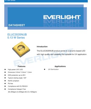
1. Product Overview
The ELUC3535NUB series represents a high-reliability, ceramic-based LED solution specifically engineered for ultraviolet C (UVC) applications. This product is designed to deliver consistent performance in demanding environments where germicidal efficacy is paramount. Its core construction leverages a ceramic substrate, which provides superior thermal management compared to traditional plastic packages, a critical factor for maintaining LED lifespan and output stability in UVC applications.
The primary target market for this component is the disinfection and sterilization sector. This includes applications such as water purification systems, air sanitization devices, surface disinfection equipment, and medical instrument sterilization. The product's design prioritizes factors essential for these uses: optical power in the germicidal range, robust construction for longevity, and compatibility with standard surface-mount technology (SMT) assembly processes.
2. Technical Parameter Deep Dive
2.1 Absolute Maximum Ratings
The device is rated for a maximum DC forward current (IF) of 100 mA. However, the typical operating condition specified in the ordering information is 20 mA. This derating is crucial for ensuring long-term reliability and preventing accelerated degradation of the semiconductor junction. The maximum junction temperature (TJ) is 100°C, with a thermal resistance (Rth) from junction to ambient of 65 °C/W. This thermal resistance value is a key parameter for heatsink design; exceeding the junction temperature can lead to catastrophic failure or significantly reduced radiant flux output.
The device offers ESD protection up to 2 kV (Human Body Model), which is a standard level of protection for handling in most manufacturing environments. The operating temperature range is from -30°C to +85°C, and the storage temperature range is from -40°C to +100°C, ensuring suitability for a wide variety of global climates and storage conditions.
2.2 Photometric and Electrical Characteristics
The primary photometric output is measured in radiant flux (mW), not luminous flux (lm), as this is a non-visible UV emitter. The typical radiant flux at the nominal 20 mA drive current is 2 mW, with a minimum guaranteed value of 1 mW and a maximum of 2.5 mW for the listed order code. The peak wavelength falls within the 270 nm to 285 nm range, which is within the most effective band for germicidal action, damaging the DNA/RNA of microorganisms.
Electrically, the forward voltage (VF) at 20 mA ranges from 5.0 V to 7.5 V. This relatively high forward voltage is characteristic of deep ultraviolet LEDs. The typical viewing angle is 120°, defined as the angle where the intensity is half of the peak value (2θ1/2).
3. Binning System Explanation
The product is classified according to a detailed binning system to ensure application-specific consistency. This system covers three key parameters: Radiant Flux, Peak Wavelength, and Forward Voltage.
3.1 Radiant Flux Bins
Radiant flux is binned into three categories: Q0A (1.0-1.5 mW), Q0B (1.5-2.0 mW), and Q0C (2.0-2.5 mW). This allows designers to select LEDs based on the required optical power output for their system, with tighter tolerances than the overall minimum/maximum specs.
3.2 Peak Wavelength Bins
Peak wavelength is critically important for UVC efficacy. The bins are: U27A (270-275 nm), U27B (275-280 nm), and U28 (280-285 nm). Different pathogens have varying sensitivity peaks within the UVC spectrum, so this binning allows for optimized system design.
3.3 Forward Voltage Bins
Forward voltage is binned in 0.5V increments from 5.0V to 7.5V (e.g., 5055 for 5.0-5.5V, 5560 for 5.5-6.0V, etc.). Consistent VF within an array simplifies driver design, ensuring uniform current distribution when multiple LEDs are connected in parallel.
4. Performance Curve Analysis
4.1 Spectrum
The spectral distribution curve shows a narrow emission peak centered around the specified wavelength (e.g., ~275nm), with minimal emission outside the UVC band. This spectral purity is advantageous as it ensures energy is concentrated in the germicidal range.
4.2 Relative Radiant Flux vs. Forward Current
The curve demonstrates a sub-linear relationship. While output increases with current, the efficiency (mW/mA) decreases at higher currents due to increased junction temperature and other non-ideal effects. This highlights the importance of thermal management and operating within recommended conditions.
4.3 Forward Current vs. Forward Voltage
The I-V curve shows the exponential relationship typical of a diode. The specified VF range at 20mA is clearly indicated. The curve is essential for designing the constant-current driver, as a small change in voltage can lead to a large change in current.
4.4 Relative Radiant Flux vs. Ambient Temperature
This curve shows the negative temperature coefficient of the LED's output. As ambient (and consequently junction) temperature rises, the radiant flux decreases. This thermal droop must be accounted for in system design to ensure consistent disinfection performance over the entire operating temperature range.
4.5 Derating Curve
The derating curve is the most critical graph for reliable operation. It defines the maximum allowable forward current as a function of the ambient temperature. To prevent exceeding the maximum junction temperature, the drive current must be reduced as ambient temperature increases. For example, at an ambient temperature of 85°C, the maximum allowable current is significantly lower than the absolute maximum rating of 100mA.
5. Mechanical and Packaging Information
5.1 Mechanical Dimensions
The package has a compact footprint of 3.5 mm x 3.5 mm with a height of 1.3 mm. The dimensional drawing specifies the location of the anode (pad 2), cathode (pad 1), and the central thermal pad (pad 3). The thermal pad is essential for effective heat sinking; it must be properly soldered to a thermally conductive pad on the PCB, which should be connected to internal ground planes or an external heatsink.
5.2 Emitter Tape and Reel Packaging
The LEDs are supplied on embossed carrier tape, wound onto reels containing 1000 pieces. The tape dimensions and reel specifications (e.g., 180mm reel diameter) are provided to ensure compatibility with automated pick-and-place machines. The components are further packaged within a moisture-resistant aluminum bag containing desiccant to prevent moisture absorption during storage, which is critical for ceramic packages to avoid \"popcorning\" during reflow soldering.
6. Soldering and Assembly Guidelines
The ELUC3535NUB is suitable for standard SMT reflow soldering processes. Key recommendations include: using a lead-free reflow profile compatible with the component's thermal limits, avoiding mechanical stress on the LED during heating and cooling, and limiting the number of reflow cycles to a maximum of two. After soldering, the PCB should not be bent, as this can induce mechanical stress on the solder joints and the ceramic body, potentially leading to cracking or failure.
7. Application Suggestions and Design Considerations
7.1 Typical Application Scenarios
- Static Air Disinfection: Used in HVAC systems or air purifiers, where UVC light irradiates a chamber through which air passes.
- Surface Disinfection: Integrated into devices for sanitizing mobile phones, tools, or countertops.
- Water Sterilization: Employed in point-of-use water purifiers, where water flows past a UVC-transparent quartz sleeve containing the LED.
7.2 Critical Design Considerations
- Thermal Management: This is the single most important factor. Use a PCB with thermal vias under the thermal pad connected to large copper pours or an external heatsink. Monitor junction temperature.
- Drive Current: Operate at or below the recommended 20mA for longevity. Use a constant-current driver, not a constant-voltage source.
- Optical Materials: The output window is quartz glass. Ensure any secondary optics or protective covers are made of UVC-transmissive materials (e.g., fused silica, certain specialty plastics). Standard glass and most plastics absorb UVC radiation.
- Safety: UVC radiation is harmful to eyes and skin. Enclosures must prevent any leakage of UV light during operation. Include interlock switches if enclosures can be opened during use.
8. Technical Comparison and Differentiation
The ELUC3535NUB's primary differentiators are its ceramic package (AIN - Aluminum Nitride) and quartz glass lens. The ceramic package offers significantly better thermal conductivity than plastic (e.g., PPA, PCT), leading to lower operating junction temperatures at the same drive current, which directly translates to longer lifetime and more stable output. The quartz glass lens provides superior UV transmission and resistance to darkening (solarization) compared to silicone or epoxy lenses, which can degrade under prolonged UVC exposure.
9. Frequently Asked Questions (Based on Technical Parameters)
Q: Can I drive this LED at 100mA for higher output?
A: No. The 100mA rating is an Absolute Maximum Rating, not an operating condition. Exceeding the typical 20mA drive current will drastically increase junction temperature, leading to rapid output degradation and potential device failure. Always follow the derating curve.
Q: Why is the forward voltage so high and variable (5.0-7.5V)?
A> The high bandgap energy required to emit UVC photons results in a higher forward voltage. The variation is inherent to semiconductor manufacturing processes, which is why the binning system is provided. Design your driver circuit to accommodate the full voltage range of your selected bin.
Q: How do I interpret the \"Minimum Radiant Flux\" of 1mW?
A> This is the guaranteed lower limit for the specific order code. The typical value is 2mW, and most devices will perform near this. The binning system (Q0A/B/C) allows you to purchase parts with a tighter, guaranteed minimum within that overall range.
10. Practical Design Case Study
Scenario: Designing a compact USB-powered surface sanitizer wand.
Design Steps:
1. Power Budget: USB port provides 5V, ~500mA max. The LED VF (5-7.5V) is higher than the source. A boost converter constant-current driver is required.
2. Thermal Design: The wand housing is small. Select a high-thermal-conductivity metal core PCB (MCPCB). Solder the LED's thermal pad directly to the MCPCB. The metal base of the MCPCB acts as the primary heatsink and part of the wand body.
3. Optical Design: Use a shallow reflector to direct the 120° beam towards the target surface. Ensure the reflector material is UVC-stable (e.g., aluminum with a protective coating).
4. Safety: Design a shutter that only opens when the wand is pressed against a surface, blocking UVC leakage. Include a timer circuit to limit exposure duration per activation.
5. Component Selection: Choose LEDs from a single Forward Voltage bin (e.g., 5055) to simplify driver design if using multiple LEDs. Select the appropriate Radiant Flux bin based on the desired dose and treatment time.
11. Operating Principle
UVC LEDs are semiconductor devices that emit photons in the ultraviolet spectrum (specifically 200-280nm for UVC) through electroluminescence. When a forward voltage is applied across the p-n junction, electrons and holes are injected into the active region. Their recombination releases energy in the form of photons. The wavelength of these photons is determined by the bandgap energy of the semiconductor materials used in the active region (typically aluminum gallium nitride - AlGaN). A narrower bandgap results in longer wavelengths (visible/infrared), while the very wide bandgap needed for UVC emission is achieved with high aluminum content in the AlGaN layers.
12. Technology Trends
The UVC LED market is driven by the demand for mercury-free, instant-on, compact, and robust disinfection solutions. Key trends include:
Increasing Wall-Plug Efficiency (WPE): Research focuses on improving internal quantum efficiency (IQE) and light extraction efficiency (LEE) to convert more electrical input into UVC optical output, reducing power consumption and heat generation.
Higher Output Power: Development of multi-chip packages and improved epitaxial processes is steadily increasing the radiant flux per device, enabling treatment of larger volumes or reducing exposure time.
Longer Lifetimes: Improvements in packaging materials (like the ceramic and quartz used here), die attach techniques, and semiconductor reliability are extending the operational lifetime (L70/B50) of UVC LEDs, making them more viable for continuous-operation applications.
Cost Reduction: As manufacturing volumes increase and processes mature, the cost per milliwatt of UVC output is decreasing, broadening the range of feasible applications beyond niche markets.
LED Specification Terminology
Complete explanation of LED technical terms
Photoelectric Performance
| Term | Unit/Representation | Simple Explanation | Why Important |
|---|---|---|---|
| Luminous Efficacy | lm/W (lumens per watt) | Light output per watt of electricity, higher means more energy efficient. | Directly determines energy efficiency grade and electricity cost. |
| Luminous Flux | lm (lumens) | Total light emitted by source, commonly called "brightness". | Determines if the light is bright enough. |
| Viewing Angle | ° (degrees), e.g., 120° | Angle where light intensity drops to half, determines beam width. | Affects illumination range and uniformity. |
| CCT (Color Temperature) | K (Kelvin), e.g., 2700K/6500K | Warmth/coolness of light, lower values yellowish/warm, higher whitish/cool. | Determines lighting atmosphere and suitable scenarios. |
| CRI / Ra | Unitless, 0–100 | Ability to render object colors accurately, Ra≥80 is good. | Affects color authenticity, used in high-demand places like malls, museums. |
| SDCM | MacAdam ellipse steps, e.g., "5-step" | Color consistency metric, smaller steps mean more consistent color. | Ensures uniform color across same batch of LEDs. |
| Dominant Wavelength | nm (nanometers), e.g., 620nm (red) | Wavelength corresponding to color of colored LEDs. | Determines hue of red, yellow, green monochrome LEDs. |
| Spectral Distribution | Wavelength vs intensity curve | Shows intensity distribution across wavelengths. | Affects color rendering and quality. |
Electrical Parameters
| Term | Symbol | Simple Explanation | Design Considerations |
|---|---|---|---|
| Forward Voltage | Vf | Minimum voltage to turn on LED, like "starting threshold". | Driver voltage must be ≥Vf, voltages add up for series LEDs. |
| Forward Current | If | Current value for normal LED operation. | Usually constant current drive, current determines brightness & lifespan. |
| Max Pulse Current | Ifp | Peak current tolerable for short periods, used for dimming or flashing. | Pulse width & duty cycle must be strictly controlled to avoid damage. |
| Reverse Voltage | Vr | Max reverse voltage LED can withstand, beyond may cause breakdown. | Circuit must prevent reverse connection or voltage spikes. |
| Thermal Resistance | Rth (°C/W) | Resistance to heat transfer from chip to solder, lower is better. | High thermal resistance requires stronger heat dissipation. |
| ESD Immunity | V (HBM), e.g., 1000V | Ability to withstand electrostatic discharge, higher means less vulnerable. | Anti-static measures needed in production, especially for sensitive LEDs. |
Thermal Management & Reliability
| Term | Key Metric | Simple Explanation | Impact |
|---|---|---|---|
| Junction Temperature | Tj (°C) | Actual operating temperature inside LED chip. | Every 10°C reduction may double lifespan; too high causes light decay, color shift. |
| Lumen Depreciation | L70 / L80 (hours) | Time for brightness to drop to 70% or 80% of initial. | Directly defines LED "service life". |
| Lumen Maintenance | % (e.g., 70%) | Percentage of brightness retained after time. | Indicates brightness retention over long-term use. |
| Color Shift | Δu′v′ or MacAdam ellipse | Degree of color change during use. | Affects color consistency in lighting scenes. |
| Thermal Aging | Material degradation | Deterioration due to long-term high temperature. | May cause brightness drop, color change, or open-circuit failure. |
Packaging & Materials
| Term | Common Types | Simple Explanation | Features & Applications |
|---|---|---|---|
| Package Type | EMC, PPA, Ceramic | Housing material protecting chip, providing optical/thermal interface. | EMC: good heat resistance, low cost; Ceramic: better heat dissipation, longer life. |
| Chip Structure | Front, Flip Chip | Chip electrode arrangement. | Flip chip: better heat dissipation, higher efficacy, for high-power. |
| Phosphor Coating | YAG, Silicate, Nitride | Covers blue chip, converts some to yellow/red, mixes to white. | Different phosphors affect efficacy, CCT, and CRI. |
| Lens/Optics | Flat, Microlens, TIR | Optical structure on surface controlling light distribution. | Determines viewing angle and light distribution curve. |
Quality Control & Binning
| Term | Binning Content | Simple Explanation | Purpose |
|---|---|---|---|
| Luminous Flux Bin | Code e.g., 2G, 2H | Grouped by brightness, each group has min/max lumen values. | Ensures uniform brightness in same batch. |
| Voltage Bin | Code e.g., 6W, 6X | Grouped by forward voltage range. | Facilitates driver matching, improves system efficiency. |
| Color Bin | 5-step MacAdam ellipse | Grouped by color coordinates, ensuring tight range. | Guarantees color consistency, avoids uneven color within fixture. |
| CCT Bin | 2700K, 3000K etc. | Grouped by CCT, each has corresponding coordinate range. | Meets different scene CCT requirements. |
Testing & Certification
| Term | Standard/Test | Simple Explanation | Significance |
|---|---|---|---|
| LM-80 | Lumen maintenance test | Long-term lighting at constant temperature, recording brightness decay. | Used to estimate LED life (with TM-21). |
| TM-21 | Life estimation standard | Estimates life under actual conditions based on LM-80 data. | Provides scientific life prediction. |
| IESNA | Illuminating Engineering Society | Covers optical, electrical, thermal test methods. | Industry-recognized test basis. |
| RoHS / REACH | Environmental certification | Ensures no harmful substances (lead, mercury). | Market access requirement internationally. |
| ENERGY STAR / DLC | Energy efficiency certification | Energy efficiency and performance certification for lighting. | Used in government procurement, subsidy programs, enhances competitiveness. |