Table of Contents
- 1. Product Overview
- 2. Technical Parameters Deep Objective Interpretation
- 2.1 Absolute Maximum Ratings
- 2.2 Electro-Optical Characteristics
- 2.2.1 Input Characteristics
- 2.2.2 Output Characteristics
- 2.3 Transfer Characteristics
- 3. Grading System Explanation
- 4. Performance Curve Analysis
- 5. Schematic and Pin Configuration
- 6. Measurement Methodology: Static dv/dt
- 7. Application Suggestions
- 7.1 Typical Application Scenarios
- 7.2 Design Considerations
- 8. Technical Comparison and Differentiation
- 9. Common Questions Based on Technical Parameters
- 10. Practical Design Case
- 11. Operating Principle
- 12. Ordering Information
1. Product Overview
The EL303X, EL304X, EL306X, and EL308X series are families of 6-pin Dual In-line Package (DIP) photocouplers designed specifically as zero-crossing triac drivers. These devices serve as a critical interface between low-voltage logic control circuits and high-voltage AC power lines, enabling safe and efficient switching of AC loads. The core function is to provide galvanic isolation while triggering an external power triac at the zero-crossing point of the AC voltage waveform, thereby minimizing electromagnetic interference (EMI) and inrush current.
The series is differentiated primarily by its peak blocking voltage capability, ranging from 250V for the EL303X to 800V for the EL308X, making it suitable for a wide range of line voltages from 110VAC to 380VAC. A key feature is the integrated zero-crossing detection circuit, which ensures the output triac triggers only when the AC line voltage is near zero volts. This device is commonly used as the core component in Solid-State Relays (SSRs), motor controllers, and various industrial and consumer appliance controls.
2. Technical Parameters Deep Objective Interpretation
2.1 Absolute Maximum Ratings
These ratings define the stress limits beyond which permanent damage to the device may occur. Operation under these conditions is not guaranteed.
- Input Forward Current (IF): Maximum continuous current through the infrared LED is 60 mA. Exceeding this can degrade or destroy the LED.
- Input Reverse Voltage (VR): The LED can withstand a reverse bias of up to 6V.
- Input/Output Power Dissipation: The input side (PD) is rated for 100 mW, and the output side (PC) for 300 mW, with specified derating factors above 85°C ambient temperature. The total device dissipation (PTOT) is 330 mW.
- Off-State Output Terminal Voltage (VDRM): This is the critical differentiating parameter. EL303X: 250V, EL304X: 400V, EL306X: 600V, EL308X: 800V. The device must be selected with a VDRM rating higher than the peak line voltage it will block.
- Isolation Voltage (VISO): 5000 Vrms for 1 minute. This specifies the dielectric strength between the input and output sides, ensuring safety and compliance with regulatory standards.
2.2 Electro-Optical Characteristics
These parameters define the device's performance under normal operating conditions at 25°C.
2.2.1 Input Characteristics
- Forward Voltage (VF): Maximum of 1.5V at IF=30mA. This is used to calculate the required current-limiting resistor for the LED driver circuit.
- Reverse Leakage Current (IR): Maximum of 10 µA at VR=6V, indicating very low leakage in reverse bias.
2.2.2 Output Characteristics
- Peak Blocking Current (IDRM): Very low leakage current (100-500 nA max) when the output is in the off-state at rated VDRM. Lower leakage is better for power efficiency.
- Peak On-State Voltage (VTM): Maximum of 3V when the output triac is conducting 100 mA peak current. This represents the conduction loss.
- Critical Rate of Rise of Off-State Voltage (dv/dt): A minimum of 600-1000 V/µs. This parameter indicates the device's immunity to false triggering caused by fast voltage transients on the AC line. Higher values are better.
- Inhibit Voltage (VINH): Maximum of 20V. If the voltage across the output terminals exceeds this value, the zero-crossing circuit prevents triggering, even if the LED is on.
2.3 Transfer Characteristics
These parameters define the relationship between the input LED current and the output triac triggering.
- LED Trigger Current (IFT): This is the maximum current required to guarantee the output triac turns on. The series is offered in three sensitivity grades: 15 mA (ELxx1), 10 mA (ELxx2), and 5 mA (ELxx3). A lower IFT allows the use of a weaker driver circuit.
- Holding Current (IH): Typical value is 280 µA. Once triggered, the output triac will remain on as long as the current through it exceeds this value. This is important for ensuring latching behavior with inductive loads.
The recommended operating LED current lies between the max IFT for the chosen grade and the absolute maximum IF of 60 mA. Operating above IFT ensures reliable triggering but below 60 mA ensures long-term reliability.
3. Grading System Explanation
The product family uses a clear grading system based on two key parameters:
- Voltage Rating (First Digit after 'EL'): This is the primary grading.
- EL303X: 250V blocking voltage.
- EL304X: 400V blocking voltage.
- EL306X: 600V blocking voltage.
- EL308X: 800V blocking voltage.
- Sensitivity Grade (Last Digit of Part Number, 'X'): This defines the LED trigger current requirement.
- Grade '1': Maximum trigger current (IFT) = 15 mA. Least sensitive.
- Grade '2': Maximum trigger current (IFT) = 10 mA.
- Grade '3': Maximum trigger current (IFT) = 5 mA. Most sensitive.
For example, an EL3062 is a 600V-rated photocoupler with a maximum trigger current of 10 mA.
4. Performance Curve Analysis
The datasheet references typical performance curves, which are essential for understanding device behavior under non-standard conditions (e.g., temperature variations). While specific graphs are not detailed in the provided text, typical curves for such devices include:
- Forward Current vs. Forward Voltage (IF-VF): Shows the non-linear relationship of the input LED, crucial for driver design.
- Trigger Current vs. Temperature (IFT vs. Ta): The required LED current to trigger the output typically increases with decreasing temperature. This is critical for designing reliable systems that operate in cold environments.
- On-State Voltage vs. On-State Current (VTM-ITM): Illustrates the conduction characteristics of the output triac.
Designers should consult the full datasheet graphs to derate parameters appropriately for their specific operating temperature range.
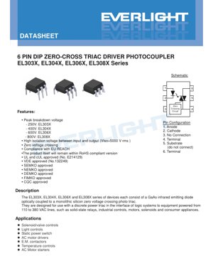
5. Schematic and Pin Configuration
The internal schematic shows an infrared GaAs LED optically coupled to a silicon chip containing the photosensitive triac and the zero-crossing detection circuitry.
Pinout (6-Pin DIP):
- Anode: Positive terminal of the input LED.
- Cathode: Negative terminal of the input LED.
- No Connection (NC): This pin is internally unconnected.
- Main Terminal 2 (MT2): One of the output triac's main terminals.
- Substrate: Internal connection. Do not connect externally.
- Main Terminal 1 (MT1): The other main terminal of the output triac. This is typically the reference point for the gate trigger signal.
The output (pins 4 and 6) is designed to be connected in series with the gate of an external, higher-power triac that actually switches the load current.
6. Measurement Methodology: Static dv/dt
The datasheet provides a detailed test circuit and procedure for measuring the Critical Rate of Rise of Off-State Voltage (dv/dt). This test is vital for quantifying the device's noise immunity.
Test Circuit: A high-voltage pulse source is connected to the Device Under Test (DUT) output via a series RC network (RTEST, CTEST). The LED is off (IF=0).
Procedure: A pulse with a peak value (VPEAK) equal to the rated VDRM is applied. The resistance RTEST is varied to change the time constant (τ = R*C) of the RC network, which in turn changes the slope (dv/dt) of the voltage ramp applied to the DUT. The slope is increased until the DUT falsely triggers. The slope is then decreased until triggering just stops. The dv/dt value at this threshold is calculated as 0.632 * VPEAK / τRC.
This measured value must meet or exceed the minimum dv/dt specification (e.g., 600 V/µs for EL308X).
7. Application Suggestions
7.1 Typical Application Scenarios
- Solid-State Relays (SSRs): The primary application, providing isolation and zero-crossing switching for AC loads like heaters, lamps, and solenoids.
- Industrial Controls: For interfacing PLC outputs with motor starters, contactors, and valve actuators.
- Consumer Appliances: Used in smart sockets, dimmers, and appliance control boards for safe AC switching.
- Temperature Controls: Switching heating elements in thermostats and ovens.
7.2 Design Considerations
- Voltage Selection: Choose a VDRM rating with a safety margin above the peak AC line voltage. For a 240VAC line (peak ~340V), an EL304X (400V) is the minimum, but an EL306X (600V) provides better margin for transients.
- LED Driver Circuit: Calculate the series resistor: R = (Vcc - VF) / I_F_operating. Ensure I_F_operating is between the max IFT (for your chosen grade) and 60mA. A typical operating current is 10-20 mA for grades 1 and 2.
- Snubber Circuits: While the photocoupler itself has a good dv/dt rating, the external power triac may require an RC snubber network across its terminals to suppress voltage spikes from inductive loads, preventing false triggering or damage.
- Heat Dissipation: Adhere to the power derating curves. The output power dissipation (PC) is primarily from the on-state voltage (VTM) multiplied by the gate current of the external triac. Ensure the total device dissipation (PTOT) is within limits at maximum ambient temperature.
8. Technical Comparison and Differentiation
The key advantages of this zero-crossing triac driver photocoupler series compared to non-zero-crossing types or basic opto-triacs are:
- Reduced EMI: By switching at the zero-crossing point, the sudden current change (di/dt) is minimized, drastically reducing conducted and radiated electromagnetic interference.
- Lower Inrush Current: Prevents high intrush currents when switching resistive loads like incandescent lamps or heating elements, extending their lifespan.
- Integrated Solution: Combines the isolation, detection, and triggering functions into one reliable 6-pin package, simplifying design compared to discrete zero-crossing circuits.
- Voltage Range: The wide range of blocking voltages (250V to 800V) covers most global AC mains applications in a single product family.
- Regulatory Compliance: The devices carry approvals from major international safety agencies (UL, cUL, VDE, etc.), simplifying end-product certification.
9. Common Questions Based on Technical Parameters
- Q: Can I use the EL303X (250V) on a 120VAC line?
A: Yes. The peak voltage of 120VAC is ~170V, which is below the 250V rating. However, for reliability against line surges, a higher-rated part like the EL304X is often recommended. - Q: What is the purpose of the "Substrate (do not connect)" pin?
A: This pin is an internal connection for the silicon die. Leaving it unconnected externally is crucial. Connecting it could short internal circuits and destroy the device. - Q: How do I choose between sensitivity grades 1, 2, and 3?
A: Grade 3 (5mA) allows the use of a higher-value current-limiting resistor or a weaker driver IC (e.g., from a microcontroller), saving power and reducing driver component stress. Grade 1 (15mA) may be chosen if the driving circuit is robust and cost of the driver is less concern, or for applications requiring higher noise immunity on the input side. - Q: The output current rating (IT(RMS)) is only 100mA. Can it switch a 10A load?
A: No. This device is a driver. The 100mA output is designed to trigger the gate of an external, much larger power triac or thyristor (e.g., a 10A or 40A TRIAC). The external component handles the full load current.
10. Practical Design Case
Scenario: Designing a solid-state relay to switch a 240VAC, 5A resistive heating element from a 5V microcontroller.
- Photocoupler Selection: Choose EL3062. 600V rating provides good margin over 340V peak. Grade 2 (10mA IFT) is a good balance between sensitivity and driver capability.
- LED Driver: Microcontroller pin (5V, 20mA max) drives the LED. VF ~1.3V. R = (5V - 1.3V) / 0.015A = ~247 Ohms. Use a 220 Ohm resistor, resulting in IF ~17mA, well above the 10mA IFT and below 60mA max.
- External Power Triac: Select a 600V, 10A+ triac (e.g., BTA16-600). Connect its Gate to pin 6 (MT1) of the photocoupler. Connect pin 4 (MT2) of the photocoupler in series with a 100-200 Ohm resistor to the AC line (via the load). This resistor limits the gate current of the power triac.
- Snubber: Add a 100 Ohm resistor and 0.1µF capacitor in series across the main terminals (A1/A2) of the BTA16 triac.
- Isolation: The 5000Vrms isolation of the photocoupler safely separates the low-voltage microcontroller circuit from the dangerous AC mains.
11. Operating Principle
The device operates on the principle of optical coupling. When a current flows through the input Infrared Light Emitting Diode (IR LED), it emits photons. These photons cross an isolation gap and strike a photosensitive silicon chip on the output side. This chip contains a light-activated triac and a zero-crossing detection circuit. The detection circuit monitors the voltage across the output terminals (MT1-MT2). Only when this voltage is below a certain threshold (typically around 20V, the inhibit voltage VINH) and the LED is illuminated, will the circuit allow the internal triac to trigger. This ensures conduction begins very close to the point where the AC sine wave crosses zero volts. Once triggered, the triac remains latched on as long as the load current exceeds its holding current (IH), until the next current zero-crossing.
12. Ordering Information
The part number follows the format: EL30XY(Z)-V
- X: Voltage series (3,4,6,8).
- Y: Sensitivity grade (1,2,3).
- Lead Form Option:
- None/M: Through-hole DIP, tube packaging.
- S / S1: Surface-mount lead form. S1 is a low-profile version.
- Tape and Reel Option (Z): TA or TB for SMD parts, specifying reel type.
- V: Indicates VDE safety approval is included.
Example: EL3062S-TA-V is a 600V, Grade 2, surface-mount device on TA tape and reel, with VDE approval.
LED Specification Terminology
Complete explanation of LED technical terms
Photoelectric Performance
| Term | Unit/Representation | Simple Explanation | Why Important |
|---|---|---|---|
| Luminous Efficacy | lm/W (lumens per watt) | Light output per watt of electricity, higher means more energy efficient. | Directly determines energy efficiency grade and electricity cost. |
| Luminous Flux | lm (lumens) | Total light emitted by source, commonly called "brightness". | Determines if the light is bright enough. |
| Viewing Angle | ° (degrees), e.g., 120° | Angle where light intensity drops to half, determines beam width. | Affects illumination range and uniformity. |
| CCT (Color Temperature) | K (Kelvin), e.g., 2700K/6500K | Warmth/coolness of light, lower values yellowish/warm, higher whitish/cool. | Determines lighting atmosphere and suitable scenarios. |
| CRI / Ra | Unitless, 0–100 | Ability to render object colors accurately, Ra≥80 is good. | Affects color authenticity, used in high-demand places like malls, museums. |
| SDCM | MacAdam ellipse steps, e.g., "5-step" | Color consistency metric, smaller steps mean more consistent color. | Ensures uniform color across same batch of LEDs. |
| Dominant Wavelength | nm (nanometers), e.g., 620nm (red) | Wavelength corresponding to color of colored LEDs. | Determines hue of red, yellow, green monochrome LEDs. |
| Spectral Distribution | Wavelength vs intensity curve | Shows intensity distribution across wavelengths. | Affects color rendering and quality. |
Electrical Parameters
| Term | Symbol | Simple Explanation | Design Considerations |
|---|---|---|---|
| Forward Voltage | Vf | Minimum voltage to turn on LED, like "starting threshold". | Driver voltage must be ≥Vf, voltages add up for series LEDs. |
| Forward Current | If | Current value for normal LED operation. | Usually constant current drive, current determines brightness & lifespan. |
| Max Pulse Current | Ifp | Peak current tolerable for short periods, used for dimming or flashing. | Pulse width & duty cycle must be strictly controlled to avoid damage. |
| Reverse Voltage | Vr | Max reverse voltage LED can withstand, beyond may cause breakdown. | Circuit must prevent reverse connection or voltage spikes. |
| Thermal Resistance | Rth (°C/W) | Resistance to heat transfer from chip to solder, lower is better. | High thermal resistance requires stronger heat dissipation. |
| ESD Immunity | V (HBM), e.g., 1000V | Ability to withstand electrostatic discharge, higher means less vulnerable. | Anti-static measures needed in production, especially for sensitive LEDs. |
Thermal Management & Reliability
| Term | Key Metric | Simple Explanation | Impact |
|---|---|---|---|
| Junction Temperature | Tj (°C) | Actual operating temperature inside LED chip. | Every 10°C reduction may double lifespan; too high causes light decay, color shift. |
| Lumen Depreciation | L70 / L80 (hours) | Time for brightness to drop to 70% or 80% of initial. | Directly defines LED "service life". |
| Lumen Maintenance | % (e.g., 70%) | Percentage of brightness retained after time. | Indicates brightness retention over long-term use. |
| Color Shift | Δu′v′ or MacAdam ellipse | Degree of color change during use. | Affects color consistency in lighting scenes. |
| Thermal Aging | Material degradation | Deterioration due to long-term high temperature. | May cause brightness drop, color change, or open-circuit failure. |
Packaging & Materials
| Term | Common Types | Simple Explanation | Features & Applications |
|---|---|---|---|
| Package Type | EMC, PPA, Ceramic | Housing material protecting chip, providing optical/thermal interface. | EMC: good heat resistance, low cost; Ceramic: better heat dissipation, longer life. |
| Chip Structure | Front, Flip Chip | Chip electrode arrangement. | Flip chip: better heat dissipation, higher efficacy, for high-power. |
| Phosphor Coating | YAG, Silicate, Nitride | Covers blue chip, converts some to yellow/red, mixes to white. | Different phosphors affect efficacy, CCT, and CRI. |
| Lens/Optics | Flat, Microlens, TIR | Optical structure on surface controlling light distribution. | Determines viewing angle and light distribution curve. |
Quality Control & Binning
| Term | Binning Content | Simple Explanation | Purpose |
|---|---|---|---|
| Luminous Flux Bin | Code e.g., 2G, 2H | Grouped by brightness, each group has min/max lumen values. | Ensures uniform brightness in same batch. |
| Voltage Bin | Code e.g., 6W, 6X | Grouped by forward voltage range. | Facilitates driver matching, improves system efficiency. |
| Color Bin | 5-step MacAdam ellipse | Grouped by color coordinates, ensuring tight range. | Guarantees color consistency, avoids uneven color within fixture. |
| CCT Bin | 2700K, 3000K etc. | Grouped by CCT, each has corresponding coordinate range. | Meets different scene CCT requirements. |
Testing & Certification
| Term | Standard/Test | Simple Explanation | Significance |
|---|---|---|---|
| LM-80 | Lumen maintenance test | Long-term lighting at constant temperature, recording brightness decay. | Used to estimate LED life (with TM-21). |
| TM-21 | Life estimation standard | Estimates life under actual conditions based on LM-80 data. | Provides scientific life prediction. |
| IESNA | Illuminating Engineering Society | Covers optical, electrical, thermal test methods. | Industry-recognized test basis. |
| RoHS / REACH | Environmental certification | Ensures no harmful substances (lead, mercury). | Market access requirement internationally. |
| ENERGY STAR / DLC | Energy efficiency certification | Energy efficiency and performance certification for lighting. | Used in government procurement, subsidy programs, enhances competitiveness. |