Table of Contents
- 1. Product Overview
- 2. Technical Parameter Deep Dive
- 2.1 Absolute Maximum Ratings
- 2.2 Electro-Optical Characteristics
- 2.2.1 Input Characteristics
- 2.2.2 Output Characteristics
- 2.2.3 Transfer Characteristics
- 3. Performance Curve Analysis
- 4. Mechanical and Package Information
- 4.1 Package Dimensions
- 4.2 Polarity Identification and Marking
- 4.3 Recommended SMD Pad Layout
- 5. Soldering and Assembly Guidelines
- 6. Packaging and Ordering Information
- 6.1 Ordering Code Structure
- 6.2 Tape and Reel Specifications
- 7. Application Suggestions
- 7.1 Typical Application Circuits
- 7.2 Design Considerations
- 8. Technical Comparison and Differentiation
- 9. Frequently Asked Questions (Based on Technical Parameters)
- 10. Practical Design Case Study
- 11. Operating Principle
- 12. Technology Trends
1. Product Overview
The EL815 series represents a family of high-performance photodarlington photocouplers (optocouplers) housed in a compact 4-pin Dual In-line Package (DIP). The core function of this device is to provide electrical isolation and signal transmission between two circuits with different potentials or impedances. It achieves this by utilizing an infrared light-emitting diode (LED) on the input side, which is optically coupled to a photodarlington transistor on the output side. This design ensures complete galvanic isolation, preventing ground loops and protecting sensitive circuitry from voltage spikes or noise originating in the other circuit.
The photodarlington configuration provides a very high current transfer ratio (CTR), making it highly sensitive and suitable for applications where a small input current needs to control a larger output current. A key advantage of this series is its compliance with various international safety and environmental standards, including halogen-free requirements, RoHS, and EU REACH, making it suitable for global markets and environmentally conscious designs.
2. Technical Parameter Deep Dive
2.1 Absolute Maximum Ratings
These ratings define the limits beyond which permanent damage to the device may occur. They are not intended for normal operation.
- Input Forward Current (IF): 60 mA (DC). This is the maximum continuous current that can be driven through the input infrared LED.
- Peak Forward Current (IFP): 1 A for 1 µs pulse. The LED can withstand short, high-current pulses, which is useful for certain switching or transient conditions.
- Input Reverse Voltage (VR): 6 V. The maximum reverse-bias voltage that can be applied across the input LED.
- Collector-Emitter Voltage (VCEO): 35 V. The maximum voltage that can be sustained between the collector and emitter of the output photodarlington transistor when the base is open.
- Collector Current (IC): 80 mA. The maximum continuous current the output transistor can sink.
- Total Power Dissipation (PTOT): 200 mW. The maximum combined power that can be dissipated by the input and output sections of the device.
- Isolation Voltage (VISO): 5000 Vrms for 1 minute. This critical parameter specifies the high-voltage isolation capability between the input and output sides, tested with pins 1-2 shorted and pins 3-4 shorted.
- Operating Temperature (TOPR): -55°C to +110°C. The ambient temperature range over which the device is specified to operate.
2.2 Electro-Optical Characteristics
These parameters are measured under specified test conditions (typically Ta = 25°C) and define the device's performance.
2.2.1 Input Characteristics
- Forward Voltage (VF): Typically 1.2V, maximum 1.4V at IF = 20 mA. This is the voltage drop across the infrared LED when driven.
- Reverse Current (IR): Maximum 10 µA at VR = 4V. The small leakage current when the LED is reverse-biased.
2.2.2 Output Characteristics
- Collector-Emitter Dark Current (ICEO): Maximum 1 µA at VCE = 10V, IF = 0mA. The leakage current of the output transistor when the input LED is off.
- Collector-Emitter Saturation Voltage (VCE(sat)): Typically 0.8V, maximum 1.0V at IF = 20mA, IC = 5mA. The voltage across the output transistor when it is fully turned on (saturated). A lower value is desirable for minimizing power loss.
2.2.3 Transfer Characteristics
- Current Transfer Ratio (CTR): 600% (Min) to 7500% (Max) at IF = 1mA, VCE = 2V. This is the most important parameter for a photocoupler, defined as (IC / IF) * 100%. The extremely wide range indicates the device is available in multiple sensitivity grades. A high CTR allows for efficient signal transfer with minimal input drive current.
- Isolation Resistance (RIO): Minimum 5 x 10¹⁰ Ω at VIO = 500V DC. This indicates the extremely high DC resistance between the isolated sides.
- Rise Time (tr): Typically 60 µs, maximum 300 µs. Fall Time (tf): Typically 53 µs, maximum 250 µs. These parameters, along with a cut-off frequency (fc) of typically 6 kHz, define the switching speed of the device. The photodarlington structure inherently has slower switching times compared to phototransistors or photo-IC couplers, making it more suitable for DC and low-frequency AC applications rather than high-speed digital isolation.
3. Performance Curve Analysis
The datasheet includes typical characteristic curves which are essential for understanding device behavior under non-standard conditions. While the specific graphs are not reproduced in text, their implications are critical for design.
- CTR vs. Forward Current (IF): Typically, CTR decreases as forward current increases. Designers must consult this curve to select the optimal operating point for their required output current and transfer efficiency.
- CTR vs. Ambient Temperature (Ta): CTR is temperature-dependent, usually decreasing at temperature extremes. This curve is vital for ensuring reliable operation across the specified -55°C to +110°C range. Designs for harsh environments must derate performance based on this data.
- Collector Current vs. Collector-Emitter Voltage (IC-VCE): These output curves, parameterized by different input currents (IF), show the operating regions (saturation, active) of the photodarlington. They are used to determine the load line and ensure the device operates within safe and functional limits.
- Switching Time Waveforms: The test circuit and waveform diagram illustrate how rise time (tr), fall time (tf), turn-on delay (ton), and turn-off delay (toff) are measured. Understanding these helps in designing timing circuits and predicting signal integrity.
4. Mechanical and Package Information
4.1 Package Dimensions
The EL815 is offered in three primary lead form options, each with detailed mechanical drawings specifying all critical dimensions in millimeters.
- Standard DIP Type: The classic through-hole package with standard pin spacing.
- Option M Type: Features a wide lead bend, providing a 0.4-inch (approx. 10.16mm) lead spacing, which can be beneficial for creepage and clearance requirements on PCBs.
- Option S1 Type: A surface-mount device (SMD) lead form with a low profile. This is the SMD variant of the package.
All packages maintain a creepage distance greater than 7.62 mm, which contributes to the high isolation voltage rating.
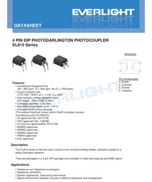
4.2 Polarity Identification and Marking
The pin configuration is standard for a 4-pin DIP photocoupler:
- Anode (Input LED positive)
- Cathode (Input LED negative)
- Emitter (Output transistor emitter)
- Collector (Output transistor collector)
The device is marked on the top with "EL" (denoting the series), "815" (the device number), followed by a 1-digit year code (Y), a 2-digit week code (WW), and an optional "V" for VDE-approved versions.
4.3 Recommended SMD Pad Layout
For the S1 (surface mount) option, the datasheet provides a suggested pad layout diagram. The dimensions are given as a reference, and the note explicitly states that designers should modify the pad dimensions based on their specific PCB manufacturing process and reliability requirements.
5. Soldering and Assembly Guidelines
The Absolute Maximum Ratings specify a soldering temperature (TSOL) of 260°C for 10 seconds. This is a critical parameter for reflow soldering processes.
- Reflow Soldering: For SMD (S1 option) assembly, a standard lead-free reflow profile with a peak temperature not exceeding 260°C for the specified time should be used. The profile must be controlled to avoid thermal shock.
- Wave/Hand Soldering: For through-hole (Standard and M option) packages, standard wave or hand soldering techniques can be used, but care should be taken to limit the exposure time of the device body to high temperature.
- Storage Conditions: The storage temperature range is specified as -55°C to +125°C. Devices should be stored in a dry, anti-static environment. For SMD parts supplied in tape and reel, the reel should be stored in its original moisture barrier bag with desiccant if the devices are moisture-sensitive (though not explicitly stated as MSL-rated in this datasheet).
6. Packaging and Ordering Information
6.1 Ordering Code Structure
The part number follows the format: EL815X(Z)-V
- X: Lead form option.
- None: Standard DIP-4 (100 units/tube).
- M: Wide lead bend, 0.4" spacing (100 units/tube).
- S1: Surface mount lead form, low profile.
- Z: Tape and reel option (only applicable with S1).
- TA, TB, TU, TD: Different tape and reel specifications affecting packing quantity and feed direction.
- V: Optional suffix denoting VDE safety approval.
6.2 Tape and Reel Specifications
Detailed dimensional drawings and tables are provided for the tape (carrier tape, cover tape) and the reel. Key dimensions include pocket size (A, B), hole diameter (D0), component spacing (P0), tape width (W), and reel hub dimensions. Options TA and TB differ in the direction of feed from the reel, which must be correctly configured in automated pick-and-place equipment.
7. Application Suggestions
7.1 Typical Application Circuits
The datasheet lists several application areas: telephone sets/exchanges, sequence controllers, system appliances, measuring instruments, and signal transmission between circuits of different potentials/impedances. The high CTR and isolation voltage make it particularly suitable for:
- Microcontroller I/O Isolation: Protecting a low-voltage microcontroller from higher voltage or noisy industrial control signals.
- AC Line Sensing: Using the photocoupler to provide isolated feedback from a triac or relay driving an AC load.
- Ground Loop Elimination: Breaking ground loops in analog signal chains between sensors and data acquisition systems.
- Logic Level Translation with Isolation: Interfacing logic circuits operating at different voltage levels while maintaining isolation.
7.2 Design Considerations
- Input Current Limiting: A series resistor must always be used with the input LED to limit the forward current (IF) to the desired value, calculated as (Supply Voltage - VF) / IF.
- Output Loading: The output photodarlington acts as a current sink. A pull-up resistor is typically connected from the collector to a positive supply voltage (VCC). The value of this resistor and the load will determine the output voltage swing and switching speed.
- Speed vs. Sensitivity Trade-off: The high CTR comes at the cost of slower switching speeds. This device is not suitable for high-frequency communication (e.g., digital isolators for USB, SPI > 10 kHz). It is ideal for state detection, slow control signals, and AC power line synchronization (50/60 Hz).
- Thermal Considerations:** While power dissipation is low, operating at the maximum junction temperature (inferred from TOPR up to 110°C) may require derating the maximum allowable currents or power dissipation.
8. Technical Comparison and Differentiation
The EL815 series, as a photodarlington coupler, occupies a specific niche compared to other optocoupler types:
- vs. Standard Phototransistor Couplers: Photodarlington couplers offer a much higher CTR (often 10-100x higher) but are significantly slower. Choose a phototransistor for moderate speed (tens of kHz) and a photodarlington for maximum sensitivity with low input current at low frequencies.
- vs. Photo-IC (Logic Output) Couplers: Photo-IC couplers have digital output (clean switching) and can be very fast (MBd range), but they have a fixed, often lower, current transfer function and require a specific supply voltage on the output side. The EL815 provides an analog current output and can operate over a wide range of output voltages (up to VCEO).
- vs. Other Photodarlingtons: The key differentiators of the EL815 are its high 5000Vrms isolation, wide operating temperature range (-55°C to +110°C), and compliance with major international safety approvals (UL, VDE, cUL, SEMKO, etc.). The wide CTR binning (600-7500%) allows sourcing parts tailored for specific sensitivity needs.
9. Frequently Asked Questions (Based on Technical Parameters)
Q: What is the purpose of the high isolation voltage (5000Vrms)?
A: It ensures reliable operation and safety in applications where the isolated circuits have a large potential difference, such as in offline power supplies, industrial motor controls, or medical equipment. It protects against high-voltage transients and prevents breakdown.
Q: My circuit needs to switch at 1 kHz. Is the EL815 suitable?
A: Yes, absolutely. With a typical cut-off frequency (fc) of 6 kHz and rise/fall times in the tens of microseconds, the EL815 can comfortably handle switching at 1 kHz. The output waveform will be rounded, not square, but for on/off control at this frequency, it is perfectly adequate.
Q: How do I choose the right CTR grade?
A: Select a minimum CTR that ensures your output transistor saturates (turns fully on) with your worst-case (lowest) planned input current. For example, if your design drives IF = 1mA and you need IC > 5mA to saturate the load, you need a CTR > 500%. Choosing a part from a higher CTR bin provides more design margin. Always consult the CTR vs. temperature curve for your operating conditions.
Q: Can I use this for analog signal isolation?
A> While possible, it is not ideal. The CTR of photodarlingtons is non-linear and varies significantly with temperature and forward current. For precision analog isolation, dedicated linear optocouplers or isolation amplifiers are recommended. The EL815 is best suited for digital (on/off) or low-accuracy analog isolation.
10. Practical Design Case Study
Scenario: Isolated Digital Input for a 24V PLC Module.
A Programmable Logic Controller (PLC) needs to read a 24V DC sensor signal while providing 4000V isolation for safety and noise immunity.
- Circuit Design: The 24V sensor output is connected in series with a current-limiting resistor and the EL815's input LED (pins 1-2). The resistor value is calculated for IF ≈ 5-10 mA at 24V. On the output side, the collector (pin 4) is connected via a 10kΩ pull-up resistor to the PLC's internal 3.3V logic supply. The emitter (pin 3) is connected to the PLC's internal ground. The output signal is taken from the collector.
- Component Selection: An EL815 with a CTR grade ensuring saturation at IF = 5mA is chosen. The 5000Vrms isolation and safety approvals (UL, VDE) meet industrial standards. The S1 (SMD) package is selected for high-density PCB assembly.
- Performance: When the 24V sensor is active, the LED turns on, causing the photodarlington to conduct, pulling the collector output voltage low (to VCE(sat) ≈ 0.8V), which is read as a logic '0' by the PLC. When the sensor is off, the photodarlington is off, and the pull-up resistor pulls the output to 3.3V (logic '1'). The isolation barrier protects the sensitive PLC logic from any faults or transients on the 24V sensor line.
11. Operating Principle
The EL815 operates on the fundamental principle of opto-electronic conversion. An electrical signal applied to the input side causes current (IF) to flow through the infrared Light-Emitting Diode (LED). This LED emits infrared light with an intensity proportional to the forward current. The light travels across a transparent isolation gap within the package and strikes the base region of a photodarlington transistor on the output side.
A photodarlington is essentially two bipolar transistors connected in a Darlington configuration, where the photocurrent generated in the first transistor's base-collector junction (acting as a photodiode) is amplified by the second transistor. This structure provides very high current gain (hFE), which translates into the observed high Current Transfer Ratio (CTR). The output collector current (IC) is thus controlled by the input light intensity, and hence by the input electrical signal, without any electrical connection between the two sides.
12. Technology Trends
Photocoupler technology continues to evolve. While traditional devices like the EL815 remain vital for cost-sensitive, high-isolation, and high-CTR applications, several trends are notable:
- Integration: Newer devices integrate additional components like base-emitter resistors on the output transistor to improve temperature stability and switching speed.
- High-Speed Digital Isolation: Technologies based on RF couplers, giant magnetoresistance (GMR), or capacitive coupling are challenging optocouplers in high-speed data isolation (≥1 Mbps) due to their superior speed, stability, and longevity.
- Miniaturization: There is a continuous push for smaller SMD packages (e.g., SO-4, SO-5) with the same or better isolation ratings, driven by the need for higher PCB density.
- Enhanced Reliability: Focus on improving long-term CTR degradation, especially under high-temperature and high-current stress conditions, to meet the demands of automotive and industrial applications with longer lifespans.
Despite these trends, the fundamental photodarlington coupler, as exemplified by the EL815 series, maintains a strong position in the market due to its simplicity, robustness, high isolation capability, and excellent performance in its intended low-to-moderate frequency domain.
LED Specification Terminology
Complete explanation of LED technical terms
Photoelectric Performance
| Term | Unit/Representation | Simple Explanation | Why Important |
|---|---|---|---|
| Luminous Efficacy | lm/W (lumens per watt) | Light output per watt of electricity, higher means more energy efficient. | Directly determines energy efficiency grade and electricity cost. |
| Luminous Flux | lm (lumens) | Total light emitted by source, commonly called "brightness". | Determines if the light is bright enough. |
| Viewing Angle | ° (degrees), e.g., 120° | Angle where light intensity drops to half, determines beam width. | Affects illumination range and uniformity. |
| CCT (Color Temperature) | K (Kelvin), e.g., 2700K/6500K | Warmth/coolness of light, lower values yellowish/warm, higher whitish/cool. | Determines lighting atmosphere and suitable scenarios. |
| CRI / Ra | Unitless, 0–100 | Ability to render object colors accurately, Ra≥80 is good. | Affects color authenticity, used in high-demand places like malls, museums. |
| SDCM | MacAdam ellipse steps, e.g., "5-step" | Color consistency metric, smaller steps mean more consistent color. | Ensures uniform color across same batch of LEDs. |
| Dominant Wavelength | nm (nanometers), e.g., 620nm (red) | Wavelength corresponding to color of colored LEDs. | Determines hue of red, yellow, green monochrome LEDs. |
| Spectral Distribution | Wavelength vs intensity curve | Shows intensity distribution across wavelengths. | Affects color rendering and quality. |
Electrical Parameters
| Term | Symbol | Simple Explanation | Design Considerations |
|---|---|---|---|
| Forward Voltage | Vf | Minimum voltage to turn on LED, like "starting threshold". | Driver voltage must be ≥Vf, voltages add up for series LEDs. |
| Forward Current | If | Current value for normal LED operation. | Usually constant current drive, current determines brightness & lifespan. |
| Max Pulse Current | Ifp | Peak current tolerable for short periods, used for dimming or flashing. | Pulse width & duty cycle must be strictly controlled to avoid damage. |
| Reverse Voltage | Vr | Max reverse voltage LED can withstand, beyond may cause breakdown. | Circuit must prevent reverse connection or voltage spikes. |
| Thermal Resistance | Rth (°C/W) | Resistance to heat transfer from chip to solder, lower is better. | High thermal resistance requires stronger heat dissipation. |
| ESD Immunity | V (HBM), e.g., 1000V | Ability to withstand electrostatic discharge, higher means less vulnerable. | Anti-static measures needed in production, especially for sensitive LEDs. |
Thermal Management & Reliability
| Term | Key Metric | Simple Explanation | Impact |
|---|---|---|---|
| Junction Temperature | Tj (°C) | Actual operating temperature inside LED chip. | Every 10°C reduction may double lifespan; too high causes light decay, color shift. |
| Lumen Depreciation | L70 / L80 (hours) | Time for brightness to drop to 70% or 80% of initial. | Directly defines LED "service life". |
| Lumen Maintenance | % (e.g., 70%) | Percentage of brightness retained after time. | Indicates brightness retention over long-term use. |
| Color Shift | Δu′v′ or MacAdam ellipse | Degree of color change during use. | Affects color consistency in lighting scenes. |
| Thermal Aging | Material degradation | Deterioration due to long-term high temperature. | May cause brightness drop, color change, or open-circuit failure. |
Packaging & Materials
| Term | Common Types | Simple Explanation | Features & Applications |
|---|---|---|---|
| Package Type | EMC, PPA, Ceramic | Housing material protecting chip, providing optical/thermal interface. | EMC: good heat resistance, low cost; Ceramic: better heat dissipation, longer life. |
| Chip Structure | Front, Flip Chip | Chip electrode arrangement. | Flip chip: better heat dissipation, higher efficacy, for high-power. |
| Phosphor Coating | YAG, Silicate, Nitride | Covers blue chip, converts some to yellow/red, mixes to white. | Different phosphors affect efficacy, CCT, and CRI. |
| Lens/Optics | Flat, Microlens, TIR | Optical structure on surface controlling light distribution. | Determines viewing angle and light distribution curve. |
Quality Control & Binning
| Term | Binning Content | Simple Explanation | Purpose |
|---|---|---|---|
| Luminous Flux Bin | Code e.g., 2G, 2H | Grouped by brightness, each group has min/max lumen values. | Ensures uniform brightness in same batch. |
| Voltage Bin | Code e.g., 6W, 6X | Grouped by forward voltage range. | Facilitates driver matching, improves system efficiency. |
| Color Bin | 5-step MacAdam ellipse | Grouped by color coordinates, ensuring tight range. | Guarantees color consistency, avoids uneven color within fixture. |
| CCT Bin | 2700K, 3000K etc. | Grouped by CCT, each has corresponding coordinate range. | Meets different scene CCT requirements. |
Testing & Certification
| Term | Standard/Test | Simple Explanation | Significance |
|---|---|---|---|
| LM-80 | Lumen maintenance test | Long-term lighting at constant temperature, recording brightness decay. | Used to estimate LED life (with TM-21). |
| TM-21 | Life estimation standard | Estimates life under actual conditions based on LM-80 data. | Provides scientific life prediction. |
| IESNA | Illuminating Engineering Society | Covers optical, electrical, thermal test methods. | Industry-recognized test basis. |
| RoHS / REACH | Environmental certification | Ensures no harmful substances (lead, mercury). | Market access requirement internationally. |
| ENERGY STAR / DLC | Energy efficiency certification | Energy efficiency and performance certification for lighting. | Used in government procurement, subsidy programs, enhances competitiveness. |