Table of Contents
- 1. Product Overview
- 2. Detailed Technical Parameters
- 2.1 Absolute Maximum Ratings
- 2.2 Electro-Optical Characteristics
- 2.2.1 Input Characteristics (LED Side)
- 2.2.2 Output Characteristics (Phototransistor Side)
- 2.2.3 Transfer Characteristics
- 3. Performance Curve Analysis
- 4. Mechanical and Packaging Information
- 4.1 Package Options and Dimensions
- 4.2 Pin Configuration and Polarity
- 4.3 Recommended PCB Pad Layout
- 5. Soldering and Assembly Guide
- 6. Packaging and Ordering Information
- 7. Application Recommendations
- 7.1 Typical Application Scenarios
- 7.2 Design Considerations
- 8. Technical Comparison and Positioning
- 9. Frequently Asked Questions (Based on Technical Parameters)
- 10. Practical Design Cases
- 11. How It Works
- 12. Technology Trends
1. Product Overview
EL2514-G serisi, yüksek performanslı 4 pinli Çift Sıralı Diziliş Paketli (DIP) fototransistör tipi optokuplörlerdir. Bu cihazlar, iki devre arasında güvenilir elektriksel izolasyon ve sinyal iletimi sağlamak üzere tasarlanmıştır. Temel bileşeni, bir silikon fototransistör dedektörüne optik olarak bağlanmış bir kızılötesi ışık yayan diyottur. EL2514-G'in önemli bir tasarım özelliği, yük direnci kiloohm seviyelerinde olsa bile göreceli olarak yüksek anahtarlama hızları için optimize edilmiş olmasıdır. Bu, onu hem izolasyon hem de orta bant genişliği gerektiren uygulamalar için uygun kılar.
The series is characterized by compliance with stringent environmental and safety standards. It is manufactured using a halogen-free process, with bromine (Br) and chlorine (Cl) content meeting specific limits. Furthermore, it has obtained certifications from major international safety agencies including UL, cUL, VDE, SEMKO, NEMKO, DEMKO, FIMKO, and CQC, ensuring its suitability for global markets and regulated applications.
2. Detailed Technical Parameters
2.1 Absolute Maximum Ratings
This device is designed to operate reliably within specified limits. Exceeding these absolute maximum ratings may cause permanent damage. Key ratings include: continuous forward current (IF) for the input LED is 50 mA, and the peak forward current (IFP) is 0.5 A, and the reverse voltage (VR) is 6 V. On the output side, the collector current (IC) is rated at 20 mA, and the collector-emitter voltage (VCEO) is 40 V. The total power consumption (PTOT) is 200 mW. A key safety parameter is the isolation voltage (VISO) is 5000 Vrms, under specific humidity conditions (40-60% RH), with input and output pins short-circuited respectively, test for 1 minute. The operating temperature range is wide, from -55°C to +110°C.
2.2 Electro-Optical Characteristics
These parameters define the performance of the device under normal operating conditions at 25°C.
2.2.1 Input Characteristics (LED Side)
- Forward Voltage (VF):The typical value is 1.2 V, with a maximum of 1.4 V when driven at IF= 20 mA. This is crucial for designing the power supply voltage of the drive circuit.
- Reverse current (IR):at VR= 4V is a maximum of 10 µA, indicating good diode characteristics.
- Input capacitance (Cin):The capacitance ranges from a typical 30 pF to a maximum of 250 pF. This capacitance affects the high-frequency drive capability.
2.2.2 Output Characteristics (Phototransistor Side)
- Collector-Emitter Dark Current (ICEO):When the LED is off and VCE= 10V, the maximum is 100 nA. This low leakage current is crucial for achieving a good "off" state.
- Collector-Emitter Breakdown Voltage (BVCEO):Minimum 40 V, measured under IC= 0.1 mA condition.
- Emitter-Collector Breakdown Voltage (BVECO):The minimum is 0.45 V, which is relatively low, indicating the asymmetry of the phototransistor.
2.2.3 Transfer Characteristics
- Current Transfer Ratio (CTR):This is a core performance metric, defined as (IC/ IF) * 100%. For the EL2514-G, under standard test conditions IF= 5 mA and VCEAt 5V, the CTR range is 50% to 200%. This wide range requires appropriate circuit design to accommodate variations between devices.
- Collector-Emitter Saturation Voltage (VCE(sat)):At IF= 5 mA and IC= 0.4 mA, maximum 0.35 V. Low saturation voltage is beneficial for achieving a strong logic low-level output.
- Isolation resistor (RIO):At 500 V10The minimum is 5 x 10DCΩ, ensuring excellent DC isolation.
- Floating capacitance (CIO):Typical value is 0.6 pF, maximum is 1.0 pF. This low capacitance helps improve common-mode transient immunity.
- Switching time:at Von) and turn-off time (toffThe maximum specification for both is 25 µs. This defines the speed at which the device operates for digital signal transmission.CC= 5V, IF= 5 mA, RL= 5 kΩ test conditions, turn-on time (t
3. Performance Curve Analysis
The datasheet references typical optoelectronic characteristic curves. While the provided text does not detail specific charts, such curves typically illustrate the relationship between key parameters. Designers should expect to see curves describing the following:
- The relationship between CTR and forward current (IF):Shows how the Current Transfer Ratio varies with different LED drive currents.
- CTR versus ambient temperature (TA):Explain the temperature dependence of CTR, which typically decreases as temperature increases.
- Collector current (IC) versus collector-emitter voltage (VCE):A family of curves for different LED currents, showing the output characteristics of the phototransistor.
- Switch waveform:Provides test circuit and related waveforms (Figure 7) to define the conditions for measuring tonand toff. This typically involves a pulse generator driving an LED, and an oscilloscope monitoring the phototransistor output across a load resistor.
Analyzing these curves is crucial for optimizing circuit performance within the expected operating temperature and current range.
4. Mechanical and Packaging Information
4.1 Package Options and Dimensions
EL2514-G offers various 4-pin DIP package variants to accommodate different assembly processes:
- Standard DIP:Classic through-hole package.
- Option M:Features "wide lead bend" providing a 0.4-inch (approximately 10.16 mm) lead pitch, which may be useful for specific PCB layout or creepage distance requirements.
- Option S1:A surface-mount (SMD) pin form with a low-profile shape. It offers two tape-and-reel packaging options (TU, TD), with 1500 devices per reel.
- Option S2:Another surface-mount pin form, also with a low-profile shape, and the tape-and-reel packaging option contains 2000 devices per reel.
Detailed dimensional drawings are provided for each package type, including key dimensions such as body size, lead length, lead pitch, and standoff height. The creepage distance between the input and output sides is specified to be greater than 7.62 mm, which contributes to achieving a high isolation rating.
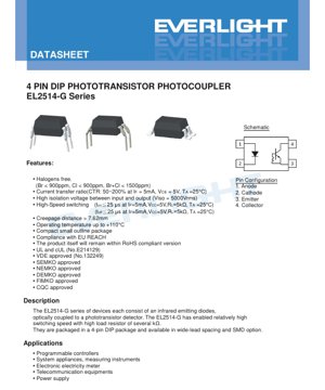
4.2 Pin Configuration and Polarity
The device uses a standard 4-pin DIP pin arrangement:
- Pin 1: Anode (Input LED)
- Pin 2: Cathode (Input LED)
- Pin 3: Emitter (Output Phototransistor)
- Pin 4: Collector (Output Phototransistor)
4.3 Recommended PCB Pad Layout
For surface mount options (S1 and S2), the datasheet provides recommended pad layouts. These are reference designs intended to ensure reliable soldering and mechanical stability. The document explicitly states that these dimensions should be modified according to specific manufacturing processes and requirements, such as solder paste volume and thermal relief considerations.
5. Soldering and Assembly Guide
The soldering temperature (TSOL) rating for this device is 260°C for a maximum of 10 seconds. This is consistent with typical lead-free reflow profiles. For through-hole packages using wave soldering, standard industry practices should be followed, taking care not to exceed the maximum body temperature of the package. The storage temperature range is -55°C to +125°C. For SMD assembly, it is recommended to store the device in moisture barrier packaging, and if the moisture exposure level is exceeded, proper baking procedures should be followed.
6. Packaging and Ordering Information
The ordering code follows the pattern: EL2514X(Y)-VG.
- X:Pin form options (S1, S2, M, or blank for standard DIP).
- Y:Tape and reel packaging options (TU, TD, or leave blank for tube).
- V:Indicates VDE safety certification (optional).
- G:Indicates halogen-free construction.
7. Application Recommendations
7.1 Typical Application Scenarios
EL2514-G is very suitable for applications requiring electrical isolation, noise immunity, or level shifting. Specific applications mentioned include:
- Programmable Logic Controller (PLC):Used to isolate digital I/O modules from the central processing unit and field devices.
- System Equipment and Measuring Instruments:Isolate sensor signals or communication lines in industrial equipment.
- Electronic energy meter:Provide isolation in metering circuits to ensure safety and suppress noise.
- Telecommunication equipment:Signal isolation in data lines or power supply feedback loops.
- Power supply:Commonly used in the feedback loop of Switch-Mode Power Supplies (SMPS) to isolate the feedback signal from the secondary side from the controller on the primary side, thereby improving safety and stability.
7.2 Design Considerations
- CTR Variation:When designing the receiving circuit (e.g., comparator threshold, pull-up resistor value), ensure reliable operation across the entire CTR range of 50-200%.
- Speed and Load:Switching speed is specified with a 5 kΩ load. Using a smaller load resistor generally increases switching speed but reduces output swing and increases power consumption. Larger resistors slow the response, especially the turn-off time, due to the phototransistor's storage time.
- LED Current Limiting:Be sure to use a series resistor to limit the forward current (IF) within the recommended operating range (typically 5-7 mA) or below the absolute maximum rating. This ensures long-term reliability and stable CTR.
- Noise Immunity:Although optocouplers provide excellent common-mode rejection, proper PCB layout should be maintained by keeping input and output traces separate and using bypass capacitors near the device pins to suppress high-frequency noise.
8. Technical Comparison and Positioning
EL2514-G distinguishes itself in the market by combining key attributes. Its high isolation voltage (5000 Vrms) and long creepage distance make it a strong candidate for applications with stringent safety requirements. The halogen-free construction meets environmental regulations and customer preferences for "green" electronics. The extensive portfolio of certifications (UL, VDE, etc.) lowers certification barriers for end products targeting global markets. While its switching speed (25 µs) is suitable for many digital isolation and power supply feedback applications, it is not positioned as an ultra-high-speed coupler for data communication; such applications require devices with nanosecond switching times. Therefore, EL2514-G is best viewed as a rugged, general-purpose optocoupler optimized for reliability, safety compliance, and moderate performance.
9. Frequently Asked Questions (Based on Technical Parameters)
Q: What does a CTR range of 50-200% mean for my circuit design?
A: This means the output current can be as low as half of the input current, or as high as twice that. Your circuit must function correctly under both extremes. For digital interfaces, this affects the selection of pull-up resistors and the input thresholds of subsequent gates or microcontrollers.
Q: Can I drive the LED directly with a voltage source?
A: No. LED is a current-driven device. You must always use a current-limiting resistor in series with the LED to set the desired IFand prevent overcurrent damage, even if your power supply voltage matches the typical VF.
Q: The isolation voltage is 5000 Vrms. Does this mean I can continuously apply 5000V between the input and output?
A: No. This is the withstand voltage tested for one minute under controlled conditions. The continuous working voltage in the application should be significantly lower than this, as defined by the relevant safety standards for the end equipment.
Q: What is the difference between option S1 and S2?
A: The main differences are in the package size and tape reel size. S2 has a slightly larger body width (B0 dimension) and uses a wider tape reel (16mm for S1, 24mm for S2), allowing more devices per reel (1500 for S1, 2000 for S2). The choice depends on your PCB space constraints and the compatibility with your assembly line's feeder.
10. Practical Design Cases
Scenario: Isolate the digital signal of the microcontroller to the high-voltage section.
A microcontroller (3.3V logic) needs to send an ON/OFF signal to a circuit operating at a different and noisy high-voltage potential. The EL2514-G can be used for isolation.
Design Steps:
- Input side:Through a current limiting resistor (RlimitConnect the microcontroller GPIO pin to the anode of the optocoupler. Calculate Rlimit= (VCC_MCU- VF) / IF. For VCC_MCU=3.3V, VF~1.2V, target IF=5mA, then Rlimit= (3.3-1.2)/0.005 = 420Ω. Use a standard 470Ω resistor. Connect the cathode to ground.
- Output side:Connect the collector to a pull-up resistor (RL) on an isolated high-voltage power supply (e.g., 12V). Connect the emitter to the isolated ground. RLThe value affects speed and current. Using the 5kΩ resistor from the datasheet test conditions provides the specified switching times. The signal from the collector node can then drive the MOSFET gate on the isolated side or another logic input.
- Layout:Physically separate the input and output sections on the PCB. Maintain a creepage distance greater than 7.62 mm according to package capability. Place a small bypass capacitor (e.g., 0.1µF) close to the device pins between the supply and ground on both sides of the coupler.
11. How It Works
An optocoupler is a device that uses light to transmit electrical signals between two isolated circuits. In the EL2514-G, the current applied to the input pins (1 and 2) causes an infrared light-emitting diode (LED) to emit photons. These photons pass through a transparent insulating gap (typically made of molding compound) and strike the base region of a silicon phototransistor on the output side (pins 3 and 4). The incident light generates electron-hole pairs in the base region, effectively acting as a base current. This photogenerated base current is then amplified by the transistor's gain, producing a collector current (IC) proportional to the input LED current (IF). The ratio IC/IFIt is the Current Transfer Ratio (CTR). The key point is that the only connection between the input and output is the light beam, thereby providing electrical isolation.
12. Technology Trends
The optocoupler market continues to evolve. Trends affecting devices such as the EL2514-G include:
- Ƙaruwar Haɗin kai:Haɗa tashoshi masu keɓewa da yawa tare, ko haɗa ayyuka ƙari kamar direban ƙofar ko mai ƙara kuskure a cikin fakitin guda ɗaya.
- Haɓaka masu haɗawa waɗanda ke amfani da na'urori masu gano sauri (kamar photodiodes tare da masu ƙara haɗin kai) don tallafawa ka'idojin sadarwar dijital na ƙimar Mbps (USB, CAN, RS-485).Enhancing Reliability and Lifespan:
- Focus on improving the long-term stability of CTR, which degrades over time due to LED aging, especially under high temperature and high current conditions.Stricter Environmental Compliance:
- Beyond RoHS and halogen-free, there is growing attention in the supply chain towards substances like PFAS and broader sustainability metrics.Alternative Isolation Technologies:
- While optocouplers still dominate in many applications, capacitive isolation (using SiObarrier) and magnetic isolation (using transformers) are competing in areas requiring extremely high speed, low power consumption, or high integration density. Optocouplers maintain advantages in simplicity, high common-mode transient immunity (CMTI), and established safety certifications.2EL2514-G focuses on safety certification, environmental compliance, and robust performance, meeting the enduring needs in industrial, power, and equipment markets where these trends are crucial.
Detailed Explanation of LED Specification Terminology
Complete Explanation of LED Technical Terminology
I. Core Indicators of Photoelectric Performance
| Terminology | Unit/Representation | Popular Explanation | Why It Is Important |
|---|---|---|---|
| Luminous Efficacy | lm/W (lumens per watt) | The luminous flux emitted per watt of electrical energy, the higher the more energy-efficient. | Directly determines the energy efficiency grade and electricity cost of the luminaire. |
| Luminous Flux | lm (lumen) | The total amount of light emitted by a light source, commonly known as "brightness". | Determine if the lamp is bright enough. |
| Viewing Angle | ° (degrees), such as 120° | The angle at which light intensity drops to half, determining the beam width. | Affects the illumination range and uniformity. |
| Color Temperature (CCT) | K (Kelvin), e.g., 2700K/6500K | The warmth or coolness of light color; lower values are yellowish/warm, higher values are whitish/cool. | Determines the lighting ambiance and suitable application scenarios. |
| Color Rendering Index (CRI / Ra) | No unit, 0–100 | The ability of a light source to reproduce the true colors of objects. Ra≥80 is recommended. | Affects color fidelity, used in high-demand places such as shopping malls and art galleries. |
| Color Tolerance (SDCM) | MacAdam ellipse steps, e.g., "5-step" | Quantitative indicator of color consistency, the smaller the step number, the more consistent the color. | Ensure no color difference among the same batch of luminaires. |
| Dominant Wavelength | nm (nanometer), e.g., 620nm (Red) | The wavelength value corresponding to the color of a colored LED. | Determine the hue of monochromatic LEDs such as red, yellow, and green. |
| Spectral Distribution | Wavelength vs. Intensity curve | It shows the intensity distribution of light emitted by an LED across various wavelengths. | It affects color rendering and color quality. |
II. Electrical Parameters
| Terminology | Symbols | Popular Explanation | Design Considerations |
|---|---|---|---|
| Forward Voltage | Vf | Minimum voltage required to turn on an LED, similar to a "starting threshold". | The driving power supply voltage must be ≥ Vf, and the voltage adds up when multiple LEDs are connected in series. |
| Forward Current | If | The current value that makes the LED emit light normally. | Constant current drive is commonly used, where the current determines brightness and lifespan. |
| Maximum Pulse Current (Pulse Current) | Ifp | Peak current that can be withstood in a short time, used for dimming or flashing. | Pulse width and duty cycle must be strictly controlled, otherwise overheating damage will occur. |
| Reverse Voltage | Vr | The maximum reverse voltage that an LED can withstand; exceeding it may cause breakdown. | The circuit needs to prevent reverse connection or voltage surge. |
| Thermal Resistance | Rth (°C/W) | The resistance to heat flow from the chip to the solder joint. A lower value indicates better heat dissipation. | A high thermal resistance requires a more robust thermal design; otherwise, the junction temperature will increase. |
| Electrostatic Discharge Immunity (ESD Immunity) | V (HBM), such as 1000V | Anti-static strike capability, the higher the value, the less susceptible to damage from static electricity. | Anti-static measures must be implemented during production, especially for high-sensitivity LEDs. |
III. Thermal Management and Reliability
| Terminology | Key Metrics | Popular Explanation | Impact |
|---|---|---|---|
| Junction Temperature | Tj (°C) | The actual operating temperature inside the LED chip. | For every 10°C reduction, the lifespan may double; excessively high temperatures lead to lumen depreciation and color shift. |
| Lumen Depreciation | L70 / L80 (hours) | The time required for the brightness to drop to 70% or 80% of its initial value. | Directly defines the "service life" of an LED. |
| Lumen Maintenance | % (e.g., 70%) | The percentage of remaining brightness after a period of use. | Characterizes the ability to maintain brightness after long-term use. |
| Color Shift | Δu′v′ or MacAdam Ellipse | The degree of color change during use. | Affect the color consistency of the lighting scene. |
| Thermal Aging | Material performance degradation | Degradation of packaging materials due to prolonged high temperatures. | May lead to decreased brightness, color shift, or open-circuit failure. |
IV. Encapsulation and Materials
| Terminology | Common Types | Popular Explanation | Characteristics and Applications |
|---|---|---|---|
| Package Type | EMC, PPA, Ceramic | Material casing yang melindungi chip dan menyediakan antarmuka optik serta termal. | EMC tahan panas baik, biaya rendah; keramik pendinginan unggul, umur panjang. |
| Struktur chip | Frontside, Flip Chip | Chip Electrode Layout. | Flip-chip provides better heat dissipation and higher luminous efficacy, suitable for high-power applications. |
| Phosphor coating | YAG, silicate, nitride | Covered on the blue light chip, partially converted into yellow/red light, mixed into white light. | Different phosphors affect luminous efficacy, color temperature, and color rendering. |
| Lens/Optical Design | Flat, Microlens, Total Internal Reflection | Optical structure on the encapsulation surface, controlling light distribution. | Determines the emission angle and light distribution curve. |
V. Quality Control and Binning
| Terminology | Binning Content | Popular Explanation | Purpose |
|---|---|---|---|
| Luminous Flux Binning | Codes such as 2G, 2H | Grouped by brightness level, each group has a minimum/maximum lumen value. | Ensure uniform brightness for products within the same batch. |
| Voltage binning | Codes such as 6W, 6X | Grouped by forward voltage range. | Facilitates driver power matching and improves system efficiency. |
| Color Grading | 5-step MacAdam Ellipse | Group by color coordinates to ensure colors fall within a minimal range. | Ensure color consistency to avoid uneven colors within the same luminaire. |
| Color temperature binning | 2700K, 3000K, etc. | Grouped by color temperature, each group has a corresponding coordinate range. | To meet the color temperature requirements of different scenarios. |
Six, Testing and Certification
| Terminology | Standard/Test | Popular Explanation | Meaning |
|---|---|---|---|
| LM-80 | Lumen Maintenance Test | Long-term illumination under constant temperature conditions, recording brightness attenuation data. | Used to estimate LED lifespan (combined with TM-21). |
| TM-21 | Standard for Life Projection | Projecting the lifespan under actual use conditions based on LM-80 data. | Provide scientific life prediction. |
| IESNA standard | Standard of the Illuminating Engineering Society | Covers optical, electrical, and thermal testing methods. | Industry-recognized testing basis. |
| RoHS / REACH | Environmental certification | Ensure the product does not contain harmful substances (e.g., lead, mercury). | Conditions for access to the international market. |
| ENERGY STAR / DLC | Energy Efficiency Certification | Energy efficiency and performance certification for lighting products. | Yawan da ake amfani da shi a cikin sayayyar gwamnati da ayyukan tallafi, don haɓaka gasar kasuwa. |